

LM27966
White LED Driver with I2C Compatible Interface
LM27966 White LED Driver with I
August 2006
General Description
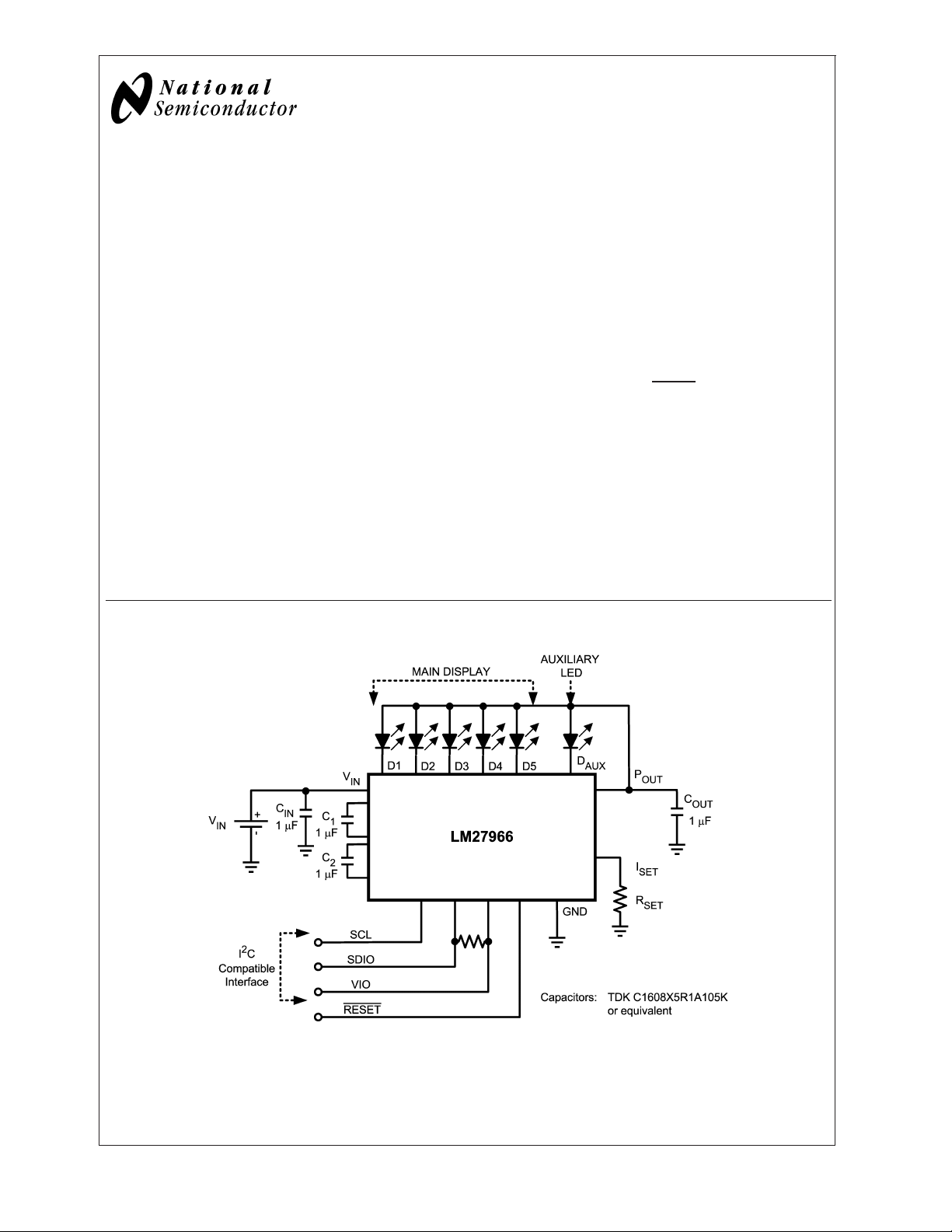
The LM27966 is a highly integrated charge-pump-based
display LED driver. The device can drive up to 6 LEDs in
parallel with a total output current of 180mA. Regulated
internal current sources deliver excellent current and brightness matching in all LEDs.
The LED driver current sources are split into two independently controlled groups. The primary group, which can be
configured with 4 or 5 LEDs, can be used to backlight the
main phone display. An additional, independently controlled
led driver is provided for driving an indicator or other general
purpose LED function. The LM27966 has an I
interface that allows the user to independently control the
brightness on each bank of LEDs.
The device provides excellent efficiency without the use of
an inductor by operating the charge pump in a gain of 3/2, or
in Pass-Mode. The proper gain for maintaining current regulation is chosen, based on LED forward voltage, so that
efficiency is maximized over the input voltage range.
The LM27966 is available in National’s small 24-pin Leadless Leadframe Package (LLP-24).
2
C compatible
Typical Application Circuit
Features
n 91% Peak LED Drive Efficiency
n No Inductor Required
n 0.3% Current Matching
n Drives 6 LEDs with up to 30mA per LED
n 180mA of total driver current
2
n I
C Compatible Brightness Control Interface
n Adaptive 1x- 3/2x Charge Pump
n Resistor-Programmable Current Settings
n External Chip RESET Pin (RESET)
n Extended Li-Ion Input: 2.7V to 5.5V
n Small low profile industry standard leadless package,
LLP 24 : (4mm x 4mm x 0.8mm)
Applications
n Mobile Phone Display Lighting
n PDAs Backlighting
n General LED Lighting
2
C Compatible Brightness Control
20190101
© 2006 National Semiconductor Corporation DS201901 www.national.com

Connection Diagram
LM27966
Pin Descriptions
Pin #s Pin Names Pin Descriptions
24 V
23 P
19, 22 (C1)
20, 21 (C2)
12, 13, 14, 15,
16
3D
17 I
1 SCL Serial Clock Pin
2 SDIO Serial Data Input/Output Pin
7 VIO Serial Bus Voltage Level Pin
10 RESET
9, 18, DAP GND Ground
4, 5, 6, 8, 11 NC No Connect
IN
OUT
C1, C2 Flying Capacitor Connections
D5, D4, D3, D2,
D1
AUX
SET
24 Pin Quad LLP Package
NS Package Number SQA24A
Input voltage. Input range: 2.7V to 5.5V.
Charge Pump Output Voltage
LED Drivers - Main Display
LED Driver - Indicator LED
Placing a resistor (R
current for Dx , and D
LED Current = 200 x (1.25V ÷ R
) between this pin and GND sets the full-scale LED
SET
LEDs.
AUX
)
SET
Harware Reset Pin. High = Normal Operation, Low = RESET
20190102
Ordering Information
Order Information Package Supplied As
LM27966SQ
LM27966SQX 4500 Units, Tape & Reel
www.national.com 2
SQA24 LLP
1000 Units, Tape & Reel
LM27966
Absolute Maximum Ratings (Notes 1, 2)
If Military/Aerospace specified devices are required,
please contact the National Semiconductor Sales Office/
Distributors for availability and specifications.
pin voltage -0.3V to 6.0V
V
IN
SCL, SDIO, VIO, RESET pin
voltages
Pin Voltages -0.3V to
I
Dx
Continuous Power Dissipation
(Note 3)
Junction Temperature (T
) 150oC
J-MAX
Storage Temperature Range -65
Maximum Lead Temperature
(Soldering)
ESD Rating(Note 5)
Human Body Model 2.0kV
-0.3V to (V
IN
w/ 6.0V max
(V
POUT
w/ 6.0V max
Internally Limited
o
C to +150oC
(Note 4)
+0.3V)
+0.3V)
Operating Rating (Notes 1, 2)
Input Voltage Range 2.7V to 5.5V
LED Voltage Range 2.0V to 4.0V
Junction Temperature (T
Ambient Temperature (T
) Range -30˚C to +100˚C
J
)
A
-30˚C to +85˚C
Range(Note 6)
Thermal Properties
Juntion-to-Ambient Thermal
Resistance (θ
), SQA24A Package
JA
(Note 7)
41.3˚C/W
ESD Caution Notice National Semiconduc-
tor recommends that all integrated circuits be handled with
appropriate ESD precautions. Failure to observe proper
ESD handling techniques can result in damage to the
device.
Electrical Characteristics (Notes 2, 8)
Limits in standard typeface are for TJ= 25˚C, and limits in boldface type apply over the full operating temperature range. Unless otherwise specified: V
= 3.6V; V
IN
Fullscale Current; EN-MAIN, EN-D5 Bits = “1”; C1=C2=1.0µF, CIN=C
current setting pins (I
Dx
and I
) apply to Main Display and Auxiliary LED. (Note 9)
SET
Symbol Parameter Condition Min Typ Max Units
Output Current Regulation
Main Display or Auxiliary LED
Enabled
I
Dx
Maximum Output Current
Regulation
Main Display and Auxiliary LED
Enabled
(Note 10)
I
Dx-MATCH
R
OUT
LED Current Matching (Note 11) 0.3 1.7 %
Open-Loop Charge Pump Output
Resistance
V
DxTH
VDx1x to 3/2x Gain Transition
Threshold
V
HR
Current Source Headroom Voltage
Requirement
(Note 12)
I
Q
I
SD
V
SET
I
Dx/
I
SET
f
SW
t
START
f
PWM
Quiescent Supply Current Gain = 1.5x, No Load 2.90 3.32 mA
Shutdown Supply Current All EN-x bits = "0" 3.4 5.4 µA
I
Pin Voltage 2.7V ≤ VIN≤ 5.5V 1.25 V
SET
Output Current to Current Set
Ratio Main Display, DAUX
Switching Frequency 0.89 1.27 1.57 MHz
Start-up Time P
Internal Diode Current PWM
Frequency
=VIN; VIO = 1.8V VDx= 0.4V; V
RESET
3.0V ≤ V
IN
≤ 5.5V
EN-AUX= ’0’
3.0V ≤ VIN≤ 5.5V
EN-AUX = ’1’ and EN-MAIN = EN-D5 = ’0’
3.2V ≤ V
R
SET
V
LED
≤ 5.5V
IN
= 8.33kΩ
= 3.6V
EN-MAIN = EN-D5 = EN-AUX = “1”
Gain = 3/2 2.75
Gain = 1 1
VDxFalling
RSET = 16.9kΩ
= 95% xI
I
Dxx
(nom) ≈ 15mA)
(I
Dxx
Dxx
Gain = 3/2
EN-MAIN = EN-D5 and/or EN-AUX= "1"
= 90% steady state 250 µs
OUT
(nom.)
= 0.4V; R
D
AUX
=1.0µF; Specifications related to output current(s) and
OUT
= 16.9kΩ;Dx=D
SET
18.2
(-9.5%)
19.2
(-7.7%)
20.1
20.8
AUX
22.0
(+9.5%)mA(%)
22.4
(+7.7%)mA(%)
30
Dx
30
D
AUX
175 mV
110 mV
200
20 kHz
=
mA
Ω
www.national.com3
Electrical Characteristics (Notes 2, 8) (Continued)
Limits in standard typeface are for TJ= 25˚C, and limits in boldface type apply over the full operating temperature range. Un-
LM27966
less otherwise specified: V
Fullscale Current; EN-MAIN, EN-D5 Bits = “1”; C1=C2=1.0µF, CIN=C
current setting pins (I
Symbol Parameter Condition Min Typ Max Units
V
RESET
Reset Voltage Thresholds 2.7V ≤ VIN≤ 5.5V Reset 0 0.45
I2C Compatible Interface Voltage Specifications (SCL, SDIO, VIO)
V
IO
V
IL
V
IH
V
OL
2
I
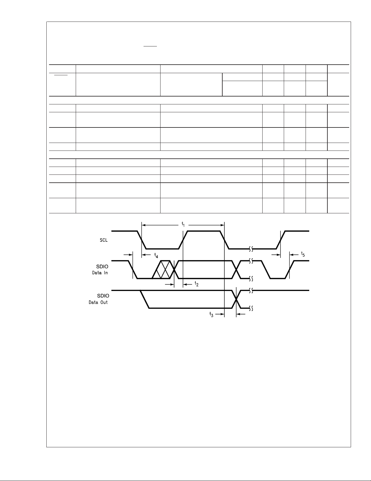
C Compatible Interface Timing Specifications (SCL, SDIO, VIO)(Note 14)
t
1
t
2
t
3
t
4
Serial Bus Voltage Level 2.7V ≤ VIN≤ 5.5V(Note 13) 1.4 V
Input Logic Low "0" 2.7V ≤ VIN≤ 5.5V, VIO = 3.0V 0 0.3 x
Input Logic High "1" 2.7V ≤ VIN≤ 5.5V, VIO = 3.0V 0.7 x
Output Logic Low "0" I
SCL (Clock Period) 2.5 µs
Data In Setup Time to SCL High 100 ns
Data Out stable After SCL Low 0 ns
SDIO Low Setup Time to SCL Low
(Start)
t
5
SDIO High Hold Time After SCL
High (Stop)
Dx
IN
and I
= 3.6V; V
) apply to Main Display and Auxiliary LED. (Note 9)
SET
=VIN; VIO = 1.8V VDx= 0.4V; V
RESET
=1.0µF; Specifications related to output current(s) and
OUT
Normal
Operation
= 3mA 400 mV
LOAD
D
AUX
= 0.4V; R
= 16.9kΩ;Dx=D
SET
1.2 V
V
IO
V
V
AUX
IN
IN
IO
IO
100 ns
100 ns
=
V
V
V
V
20190113
Note 1: Absolute Maximum Ratings indicate limits beyond which damage to the component may occur. Operating Ratings are conditions under which operation of
the device is guaranteed. Operating Ratings do not imply guaranteed performance limits. For guaranteed performance limits and associated test conditions, see the
Electrical Characteristics tables.
Note 2: All voltages are with respect to the potential at the GND pin.
Note 3: Internal thermal shutdown circuitry protects the device from permanent damage. Thermal shutdown engages at T
165˚C (typ.).
Note 4: For detailed soldering specifications and information, please refer to National Semiconductor Application Note 1187: Leadless Leadframe Package
(AN-1187).
Note 5: The human body model is a 100pF capacitor discharged through 1.5kΩ resistor into each pin. (MIL-STD-883 3015.7)
Note 6: In applications where high power dissipation and/or poor package thermal resistance is present, the maximum ambient temperature may have to be
derated. Maximum ambient temperature (T
dissipation of the device in the application (P
following equation: T
Note 7: Junction-to-ambient thermal resistance is highly dependent on application and board layout. In applications where high maximum power dissipation exists,
special care must be paid to thermal dissipation issues in board design. For more information, please refer to National Semiconductor Application Note 1187:
Leadless Leadframe Package (AN-1187).
Note 8: Min and Max limits are guaranteed by design, test, or statistical analysis. Typical numbers are not guaranteed, but do represent the most likely norm.
Note 9: C
A-MAX=TJ-MAX-OP
IN,CPOUT,C1
, and C2: Low-ESR Surface-Mount Ceramic Capacitors (MLCCs) used in setting electrical characteristics
) is dependent on the maximum operating junction temperature (T
A-MAX
), and the junction-to ambient thermal resistance of the part/package in the application (θJA), as given by the
D-MAX
–(θJAxP
D-MAX
).
= 170˚C (typ.) and disengages at TJ=
J
= 100˚C), the maximum power
J-MAX-OP
www.national.com 4
 Loading...