

Page 1
LM27961
Dual-Display White LED Driver with 3/2x Switched
Capacitor Boost
LM27961 Dual-Display White LED Driver with 3/2x Switched Capacitor Boost
November 2004
General Description
The LM27961 is a charge-pump-based white-LED driver that
is ideal for mobile phone display backlighting. It is intended
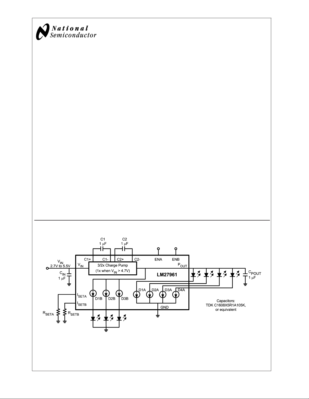
to drive 4 LEDs for a main phone display backlight and 3
LEDs for a sub-display backlight. Regulated internal current
sources deliver excellent current and brightness matching in
all LEDs.
The LED driver current sources are split into two independently controlled groups. The primary group (Group A) can
be used to backlight a main phone display with up to 4 LEDs.
The low-side current drivers of Group A accommodate
common-anode-type LEDs. The second group (Group B)
can backlight a secondary display with up to 3 LEDs. The
high-side current drivers of Group B accommodate commoncathode-type LEDs. Both Group A and Group B can also
drive standard two-terminal LEDs, and provide other general
lighting functions (keypad lighting, fun lighting, etc). The
brightness of the two LED groups can be adjusted independently with external resistors.
The LM27961 works off an extended Li-Ion input voltage
range (2.7V to 5.5V). Voltage boost is achieved with a highefficiency 3/2x-gain charge pump.
The LM27961 is available in National’s chip-scale 18-bump
micro SMD package.
Features
n Drives 4 Individual Common-Anode LEDs with up to
20mA each for a Main Display Backlight
n Drives 3 Individual Common-Cathode LEDs with up to
20mA each for a Sub-Display Backlight
n Independent Resistor-Programmable Current Setting
n Excellent Current and Brightness Matching
n High-Efficiency 3/2x Charge Pump
n Extended Li-Ion Input: 2.7V to 5.5V
n PWM Brightness Control: 100Hz - 1kHz
n 18-bump Thin Micro SMD Package:
(2.1mm x 2.4mm x 0.6mm)
Applications
n Mobile Phone Display Lighting
n Mobile Phone Keypad Lighting
n PDAs
n General LED Lighting
Typical Application Circuit
20127901
© 2004 National Semiconductor Corporation DS201279 www.national.com
Page 2

Connection Diagram
LM27961
Pin Description
Pin #s Pin Names Pin Descriptions
C1 V
D2 GND Ground
A3 P
A1, B2, A5, E1 C1+, C1-, C2+,
D6, E5, D4, E3 D1A, D2A, D3A,
C5, B4, C3 D1B, D2B, D3B LED Outputs - Group B
B6 EN-A Enable for Group-A LEDs (current outputs). Logic input.
A7 EN-B Enable for Group-B LEDs (current outputs). Logic input.
E7 I
C7 I
18-Bump Thin Micro SMD Package, Large Bump
NS Package Number TLA18
IN
OUT
Input voltage. Input range: 2.7V to 5.5V.
Charge pump output. Approximately 1.5xV
Flying capacitor connections.
C2-
LED Outputs - Group A
D4A
High = Group-A LEDs ON. Low = Group A LEDs OFF.
Pulsing this pin with a PWM signal (100Hz-1kHz) can be used to dim LEDs.
High = Group-B LEDs ON. Low = Group B LEDs OFF.
Pulsing this pin with a PWM signal (100Hz-1kHz) can be used to dim LEDs.
SETA
Placing a resistor (R
SETA
Group A LEDs. LED Current = 100 x (1.25V ÷ R
SETB
Placing a resistor (R
SETB
Group B LEDs. LED Current = 100 x (1.25V ÷ R
20127902
IN
) between this pin and GND sets the LED current for
).
SETA
) between this pin and GND sets the LED current for
).
SETB
Operational States
ENA ENB Mode of Operation
L L Shutdown
H L Enabled. Group A LEDs ON. Group B LEDs OFF
L H Enabled. Group B LEDs ON. Group A LEDs OFF
H H Invalid for normal operation
Ordering Information
Order Information Package Supplied As
LM27961TL TLA18 Micro SMD 250 Units, Tape & Reel
LM27961TLX 3000 Units, Tape & Reel
www.national.com 2
Page 3
LM27961
Absolute Maximum Ratings (Notes 1, 2)
If Military/Aerospace specified devices are required,
please contact the National Semiconductor Sales Office/
Distributors for availability and specifications.
pin voltage -0.3V to 7.1V
V
IN
ENA, ENB pin voltages -0.3V to (V
+0.3V)
IN
Operating Rating (Notes 1, 2)
Input Voltage Range 2.7V to 5.5V
Junction Temperature (T
Ambient Temperature (T
(Note 5)
) Range -30˚C to +125˚C
J
) Range
A
-30˚C to +85˚C
w/ 6.0V max
Pin Voltages -0.3V to
I
Dxx
(V
POUT
w/ 6.0V max
Continuous Power Dissipation
Internally Limited
+0.3V)
Thermal Properties
Juntion-to-Ambient Thermal
Resistance (θ
), (Note 6)
JA
100˚C/W
(Note 3)
Junction Temperature (T
Storage Temperature Range -65
Maximum Lead Temperature
) 150oC
J-MAX
o
C to +150oC
265
o
C
(Soldering, 10 sec.)
ESD Rating (Note 4)
Human Body Model - I
Human Body Model - All other Pins:
Machine Model - I
Dxx
Machine Model - All Other Pins:
Dxx
Pins:
Pins:
1.0kV
2.0kV
100V
200V
Electrical Characteristics (Notes 2, 7)
Limits in standard typeface are for TJ= 25˚C, and limits in boldface type apply over the full operating temperature range. Unless otherwise specified: V
1.5V; R
SETA=RSETB
pins (I
Dxx
and I
) apply to both Group A and Group B. (Note 8)
SETx
= 3.6V; V
IN
= 8.35kΩ;CIN,C1,C2, and C
Symbol Parameter Condition Min Typ Max Units
I
Dxx
I
Dxx-MATCH
Output Current Regulation
Current Matching Between Any
Two Group A Outputs or Group
B Outputs
I
Q
I
SD
V
SET
I
Dxx/ISET
Quiescent Supply Current 2.7V ≤ VIN≤ 4.2V;
Shutdown Supply Current 2.7V ≤ VIN≤ 5.5V,
I
Pin Voltage 2.7V ≤ VIN≤ 5.5V 1.25 V
SET
Output Current to Current Set
Ratio
= 0.6V; V
DxA
DxB
POUT
3.0V ≤ V
0.45V ≤ V
2.5V ≤ V
= 8.35kΩ
R
SET
3.0V ≤ V
0.6V ≤ V
2.5V ≤ V
= 6.25kΩ
R
SET
3.0V ≤ V
0.3V ≤ V
2.5V ≤ V
= 12.5kΩ
R
SET
2.7V ≤ V
0.45V ≤ V
2.5V ≤ V
= 8.35kΩ
R
SET
= 3.0V (Note 9) 0.6 %
V
IN
No Load Current,
ENA or ENB = ON
ENA and ENB = OFF
= 3.6V; ENA = 1.5V and ENB = GND, or ENA = GND and ENB =
= 1µF. Specifications related to output current(s) and current setting
≤ 4.2V, and VIN= 5.5V
IN
DxA
DxB
≤ 5.5V;
IN
DxA
DxB
≤ 5.5V;
IN
DxA
DxB
≤ 3.0V;
IN
DxA
DxB
≤ 3.8V or
≤ 3.8V;
≤ 3.8V or
≤ 3.8V;
≤ 3.8V or
≤ 3.8V;
≤ 3.8V or
≤ 3.8V;
13.5
(-10%)
15
16.5
(+10%)mA(%)
20 mA
10 mA
15 mA
4.4 6.75 mA
2.3 5 µA
100
www.national.com3
Page 4
Electrical Characteristics (Notes 2, 7) (Continued)
Limits in standard typeface are for TJ= 25˚C, and limits in boldface type apply over the full operating temperature range. Un-
LM27961
less otherwise specified: V
Dxx
SETA
=R
and I
SETB
) apply to both Group A and Group B. (Note 8)
SETx
1.5V; R
pins (I
Symbol Parameter Condition Min Typ Max Units
R
OUT
Charge Pump Output Resistance
(Note 10)
V
HR
Current Source Headroom
Voltage Requirement (Note 11)
f
SW
t
START
Switching Frequency 3.0V ≤ VIN≤ 4.2V 375 500 625 kHz
Start-up Time IDx= 90% steady state 350 µs
1.5x/1x Charge pump gain cross-over:
Gain = 1.5 when VINis below
threshold. Gain = 1 when V
above threshold.
Logic Pin Specifications: EN, ENA, ENB
V
IL
V
IH
I
LEAK
Note 1: Absolute Maximum Ratings indicate limits beyond which damage to the component may occur. Operating Ratings are conditions under which operation of
the device is guaranteed. Operating Ratings do not imply guaranteed performance limits. For guaranteed performance limits and associated test conditions, see the
Electrical Characteristics tables.
Note 2: All voltages are with respect to the potential at the GND pin.
Note 3: Internal thermal shutdown circuitry protects the device from permanent damage. Thermal shutdown engages at T
120˚C (typ.). The thermal shutdown function is guaranteed by design.
Note 4: The Human body model is a 100pF capacitor discharged through a 1.5kΩ resistor into each pin. The machine model is a 200pF capacitor discharged
directly into each pin. MIL-STD-883 3015.7
Note 5: In applications where high power dissipation and/or poor package thermal resistance is present, the maximum ambient temperature may have to be
derated. Maximum ambient temperature (T
dissipation of the device in the application (P
following equation: T
Note 6: Junction-to-ambient thermal resistance is highly dependent on application and board layout. In applications where high maximum power dissipation exists,
special care must be paid to thermal dissipation issues in board design.
Note 7: Min and Max limits are guaranteed by design, test, or statistical analysis. Typical numbers are not guaranteed, but do represent the most likely norm.
Note 8: C
Note 9: For the two groups of outputs on a part (GroupA and Group B), the following are determined: the maximum output current in the group (MAX), the minimum
output current in the group (MIN), and the average output current of the group (AVG). For each group, two matching numbers are calculated: (MAX-AVG)/AVG and
(AVG-MIN)/AVG. The largest number of the two (worst case) is considered the matching figure for the group. The matching figure for a given part is considered to
be the highest matching figure of the two groups. The typical specification provided is the most likely norm of the matching figure for all parts.
Note 10: Output resistance (R
V
Pout
equation applies when the charge pump is operating with a gain of 3/2 (V
Note 11: Headroom voltage: V
Note 12: There is a 300kΩ(typ.) pull-down resistor connected internally between each enable pin (ENA, ENB) and GND.
Input Logic Low 2.7V ≤ VIN≤ 5.5V 0 0.5 V
Input Logic High 2.7V ≤ VIN≤ 5.5V 1.1 V
Input Leakage Current V
A-MAX=TJ-MAX-OP
IN,CPOUT,C1
=(1.5xVIN)–(R
, and C2: Low-ESR Surface-Mount Ceramic Capacitors (MLCCs) used in setting electrical characteristics
OUTxIOUT
= 3.6V; V
IN
= 8.35kΩ;CIN,C1,C2, and C
DxA
= 0.6V; V
DxB
POUT
VIN= 3.0V 2.7 Ω
I
=95%XI
Dxx
= 8.35kΩ
R
SET
(nom) ≈ 15mA)
(I
Dxx
1.5x to 1x Threshold 4.75 V
is
1x to 1.5x Threshold 4.55 V
IN
= 0V 0.1 µA
ENx
V
= 3V (Note 12) 10
ENx
) is dependent on the maximum operating junction temperature (T
A-MAX
), and the junction-to ambient thermal resistance of the part/package in the application (θJA), as given by the
D-MAX
–(θJAxP
) models all voltage losses in the charge pump. R
OUT
). In the equation, I
HR=VPout–VLEDx
).
D-MAX
is the total output current: the sum of all active Dxx output currents and all current drawn from P
OUT
. If headroom voltage requirement is not met, LED current regulation will be compromised.
= 3.6V; ENA = 1.5V and ENB = GND, or ENA = GND and ENB =
= 1µF. Specifications related to output current(s) and current setting
(nom)
Dxx
≤ 4.75V typ.).
IN
J
J-MAX-OP
can be used to estimate the voltage at the charge pump output (P
OUT
320 mV
IN
= 160˚C (typ.) and disengages at TJ=
= 125˚C), the maximum power
OUT
V
OUT
. The
):
www.national.com 4
Page 5

LM27961
Typical Performance Characteristics Unless otherwise specified: V
= 3.6V; ENA = VINand ENB = GND, or ENA = GND and ENB = VIN;R
1µF.
LED Current (D1A, D2A,D3A, D4A)
vs. Input Voltage LED Current (DxA) vs. Input Voltage
20127904 20127905
Quiescent Current vs. Input Voltage,
SETA=RSETB
= 8.35kΩ;CIN,C1,C2, and C
Charge Pump Output Voltage
vs. Output Current
= 3.6V; V
IN
LEDxA
= 3.6V; V
POUT
LEDxB
=
20127906
20127907
www.national.com5
Page 6

Typical Performance Characteristics Unless otherwise specified: V
= 3.6V; ENA = VINand ENB = GND, or ENA = GND and ENB = VIN;R
1µF. (Continued)
LM27961
SETA=RSETB
= 3.6V; V
IN
LEDxA
= 3.6V; V
= 8.35kΩ;CIN,C1,C2, and C
POUT
LEDxB
=
Charge Pump Output Voltage
vs. Output Current
Input Current vs. Input Voltage
20127910
Charge Pump Output Voltage
vs. Input Voltage (No Load Current)
20127908
Charge Pump Output Resistance
vs Output Current
20127909
www.national.com 6
20127911
Page 7

LM27961
Typical Performance Characteristics Unless otherwise specified: V
= 3.6V; ENA = VINand ENB = GND, or ENA = GND and ENB = VIN;R
1µF. (Continued)
Charge Pump Switching Frequency
vs. Input Voltage
20127912
Diode Current (DxB)
vs. Headroom Voltage (DxB)
SETA=RSETB
vs. PWM Duty Cycle (ENA or ENB)
= 8.35kΩ;CIN,C1,C2, and C
Diode Current (DxA)
vs. Headroom Voltage (DxA)
Diode Current (DxA or DxB)
= 3.6V; V
IN
LEDxA
= 3.6V; V
POUT
20127913
LEDxB
=
20127914
20127915
www.national.com7
Page 8

Typical Performance Characteristics Unless otherwise specified: V
= 3.6V; ENA = VINand ENB = GND, or ENA = GND and ENB = VIN;R
1µF. (Continued)
LM27961
SETA=RSETB
= 3.6V; V
IN
LEDxA
= 3.6V; V
= 8.35kΩ;CIN,C1,C2, and C
POUT
LEDxB
=
Diode Current (DxA)
vs. R
SETx
20127916
ENx Signal (Top)
and Charge Pump Start-Up (Bottom) Waveforms
Input Voltage (Top)
and Output Voltage (Bottom) Waveforms
20127917
Vertical Scale = (100mV/div),
Horizontal Scale = 1µs/div)
Vertical Scale = (2V/div),
20127918
Horizontal Scale = 100µs/div)
www.national.com 8
Page 9

Block Diagram
LM27961
Circuit Description
OVERVIEW
The LM27961 is primarily intended for Lithium-Ion battery
driven white-LED drive applications, and is well suited to
drive white LEDs that are used for backlighting small-format
displays. The part has seven matched constant-current outputs, each capable of driving up to 20mA (or more) through
white LEDs. The well-matched current sources ensure the
current through all the LEDs is virtually identical. This keeps
brightness of all LEDs matched to near perfection so that
they can provide a consistent backlight over the entire display.
CHARGE PUMP
The core of the LM27961 is a 1.5x/1x dual-mode charge
pump. The input of the charge pump is connected to the V
pin. The recommended input voltage range of the LM27961
is 2.7V to 5.5V. The output of the charge pump is the P
pin (“Pump OUTput”). The output voltage of the charge
pump is unregulated and varies with input voltage and load
current.
The charge pump operates in the 1.5x mode when the input
voltage is below 4.75V (typ.). In this mode, the input-to-
OUT
20127903
output voltage gain of the charge pump is 1.5, and the
voltage at the output of the charge pump will be approximately 1.5x the input voltage (V(P
) ≈ 1.5*VIN). When in
OUT
the 1.5x mode, the charge pump provides the voltage boost
that is required to drive white LEDs from a Li-Ion battery.
(White LEDs typically have a forward voltage in the range of
3.3V to 4.0V. A Li-Ion battery typically is not considered to be
fully discharged until the battery voltage falls to 3.0V (approx.) )
The charge pump operates in the 1x mode when the input
voltage is above 4.75V (typ.). In these conditions, voltage
boost is not required to drive the LEDs, so the charge pump
merely passes the input voltage to P
OUT
(V(P
OUT
) ≈ VIN).
This reduces the input current and the power dissipation of
the LM27961 when the input voltage is high.
REGULATED CURRENT OUTPUTS
IN
The matched current outputs are generated with a precision
current mirror that is biased off the charge pump output.
Matched currents are ensured with the use of tightly
matched internal devices and internal mismatch cancellation
circuitry.
There are seven regulated current outputs. These seven
outputs are split into two groups, a group of 4 common
www.national.com9
Page 10

Circuit Description (Continued)
anode outputs and a group of 3 common cathode outputs.
LM27961
There is an ON/OFF control pin for each group (ENA and
ENB).
The DC current through the LEDs is programmed with an
external resistor. Changing currents on-the-fly can be
achieved with the use of digital pulse (PWM) signals.
ENABLE PINS: ENA, ENB
The LM27961 has 2 enable pins. Both are active-high logic
(HIGH = ON). There are internal pull-down resistors (300kΩ
typ.) that are connected internally between each of the enable pins and GND.
ENA and ENB can both enable and disable the part. When
the voltage on both pins are low (
shutdown mode. All internal circuitry is OFF and the part
consumes very little supply current when the LM27961 is
shutdown. When the voltage on either ENx pin is high
>
1.1V), the part is active. The charge pump is ON, and the
(
corresponding output current drivers are active.
ENA and ENB are used to turn the output currents ON and
OFF. ENA activates/deactivates the four GroupA outputs
(D1A-D4A). ENB activates/deactivates the three GroupB
outputs (D1B-D3B).
SETTING LED CURRENTS
The output currents of the LM27961 can be set to a desired
value simply by connecting an appropriately sized resistor
) between the I
(R
SETx
sets the current for the GroupA outputs and R
R
SETA
pins of the LM27961 and GND.
SETx
sets the current for the GroupB outputs. The output currents
(LED currents) are proportional to the current that flows out
of the I
greater than the I
pins. The output currents are a factor of 100
SETx
current. The feedback loop of an
SETx
internal amplifier sets the voltage of the I
(typ.). Placing a resistor between I
the I
current, and thus the LED currents. The statements
SETx
above are simplified in the equations below:
=100x(V
I
Dxx
= 100 x (1.25V / I
R
SETx
MAXIMUM OUTPUT CURRENT, MAXIMUM LED VOLTAGE, MINIMUM INPUT VOLTAGE
The LM27961 can drive 4 LEDs at 15mA each from an input
voltage as low as 2.7V, so long as the LEDs have a forward
voltage of 3.5V or less (room temperature).
The statement above is a simple example of the LED drive
capabilities of the LM27961. The statement contains the key
application parameters that are required to validate an LEDdrive design using the LM27961: LED current (I
ber of active LEDs (N), LED forward voltage (V
minimum input voltage (V
IN-MIN
The equation below can be used to estimate the total output
current capability of the LM27961:
I
LED_MAX
I
LED_MAX
R
= ((1.5 x VIN)-V
= ((1.5 x VIN)-V
– Output resistance. This parameter models the inter-
OUT
LED
LED
nal losses of the charge pump that result in voltage droop at
the pump output P
. Since the magnitude of the voltage
OUT
droop is proportional to the total output current of the charge
pump, the loss parameter is modeled as a resistance. The
output resistance of the LM27961 is typically 2.7Ω (V
3.0V, T
= 25˚C). In equation form:
A
<
0.5V), the part is in
SETx
and GND programs
SETx
Dxx
)
)
SETx/RSETx
).
)/((NxR
)+kHR) (eq. 1)
OUT
) / ((N x 2.7Ω) + 22mV/mA)
SETB
pin to 1.25V
), num-
LEDx
), and
LED
IN
V
= 1.5xVIN– NxI
POUT
– Headroom constant. This parameter models the mini-
k
HR
LEDxROUT
(eq. 2)
mum voltage required to be present across the current
sources for them to regulate properly. This minimum voltage
is proportional to the programmed LED current, so the constant has units of mV/mA. The typical k
of the LM27961 is
HR
22mV/mA. In equation form:
The "I
LED-MAX
the R
OUT
solving for I
(V
POUT–VLED
)>kHRxI
" equation (eq. 1) is obtained from combining
equation (eq. 2) with the kHRequation (eq. 3) and
. Maximum LED current is highly dependent
LED
LED
(eq. 3)
on minimum input voltage and LED forward voltage. Output
current capability can be increased by raising the minimum
input voltage of the application, or by selecting an LED with
a lower forward voltage. Excessive power dissipation may
also limit output current capability of an application.
PARALLEL Dx OUTPUTS FOR INCREASED CURRENT CAPABILITY
Outputs D1A through D4A, or D1B through D3B may be
connected together in any combination to drive higher currents through fewer LEDs. For example in Figure 1, outputs
D1A and D2A are connected together to drive one LED. D3A
and D4A are connected to drive a second LED.
20127919
FIGURE 1. Two Parallel Connected LEDs
With this configuration, two parallel current sources of equal
value provide current to one of the LEDs. R
SET
should
therefore be chosen so that the current through each output
is programmed to 50% of the desired current through the
parallel connected LED. For example, if 40mA is the desired
drive current for the parallel connected LED, R
SETx
should
be selected so that the current through each of the outputs is
20mA. Other combinations of parallel outputs may be implemented in similar fashions, such as in Figure 2.
=
www.national.com 10
Page 11

Circuit Description (Continued)
20127920
FIGURE 2. One Parallel Connected LED
Connecting outputs in parallel does not affect internal operation of the LM27961 and has no impact on the Electrical
Characteristics and limits previously presented. The available diode output current, maximum diode voltage, and all
other specifications provided in the Electrical Characteristics
table apply to parallel output configurations, just as they do
to the standard application circuit on pg1 of the datasheet.
SOFT START
The LM27961 contains internal soft-start circuitry to limit
input inrush currents when the part is enabled. Soft start is
implemented with a controlled turn-on of the internal voltage
reference. During soft start, the current through the LED
outputs rise at the rate of the reference voltage ramp. Due to
the soft-start circuitry, turn-on time of the LM27961 is approximately 350µs (typ.).
THERMAL PROTECTION
Internal thermal protection circuitry disables the LM27961
when the junction temperature exceeds 160˚C (typ.). This
feature protects the device from being damaged by high die
temperatures that might otherwise result from excessive
power dissipation. The device will recover and operate normally when the junction temperature falls below 120˚C (typ.).
It is important that the board layout provides good thermal
conduction. This will help to keep the junction temperature
within specified operating ratings.
Applications Information
POWER EFFICIENCY
Efficiency of LED drivers is commonly taken to be the ratio of
power consumed by the LEDs (P
the input of the part (P
current is approximately 1.5x the output current (total LED
current). For a simple approximation, the current consumed
by internal circuitry can be neglected and the efficiency of
the LM27961 can be predicted as follows:
). With a 1.5x charge pump, the input
IN
) to the power drawn at
LED
Neglecting IQwill result in a slightly higher efficiency prediction, but this impact will be no more than a few percentage
points when several LEDs are driven at full power.
ADJUSTING LED BRIGHTNESS (PWM control)
Perceived LED brightness can be adjusted using a PWM
control signal to turn the LM27961 current sources ON and
OFF at a rate faster than perceptible by the eye. When this
is done, the total brightness perceived is proportional to the
duty cycle (D) of the PWM signal (D = the percentage of time
that the LED is on in every PWM cycle). A simple example: if
the LEDs are driven at 15mA each with a PWM signal that
has a 50% duty cycle, perceived LED brightness will be
about half as bright as compared to when the LEDs are
driven continuously with 15mA. A PWM signal thus provides
brightness (dimming) control for the solution.
The minimum recommended PWM frequency is 100Hz. Frequencies below this may be visibly noticeable as flicker or
blinking. The maximum recommended PWM frequency is
1kHz. Frequencies above this may cause interference with
internal current driver circuitry.
In cases where a PWM signal must be connected to the ENx
pins, measures can be taken to reduce the magnitude of the
charge-pump turn-on voltage spikes. More input capacitance, series resistors and/or ferrite beads may provide benefits.
If the current and voltage spikes can be tolerated, connecting the PWM signal to the EN pin does provide a benefit:
lower supply current when the PWM signal is active. When
the PWM signal is low, the LM27961 will be shutdown and
input current will only be a few micro-amps. This results in a
lower time-averaged input current.
CAPACITOR SELECTION
The LM27961 requires 4 external capacitors for proper operation. Surface-mount multi-layer ceramic capacitors are
recommended. These capacitors are small, inexpensive and
have very low equivalent series resistance (ESR
typ.). Tantalum capacitors, OS-CON capacitors, and aluminum electrolytic capacitors are not recommended for use
with the LM27961 due to their high ESR, as compared to
ceramic capacitors.
For most applications, ceramic capacitors with X7R or X5R
temperature characteristic are preferred for use with the
LM27961. These capacitors have tight capacitance tolerance (as good as
ture (X7R:
-55˚C to 85˚C).
Capacitors with Y5V or Z5U temperature characteristic are
generally not recommended for use with the LM27961. Capacitors with these temperature characteristics typically
have wide capacitance tolerance (+80%, -20%) and vary
significantly over temperature (Y5V: +22%, -82% over -30˚C
to +85˚C range; Z5U: +22%, -56% over +10˚C to +85˚C
range). Under some conditions, a nominal 1µF Y5V or Z5U
capacitor could have a capacitance of only 0.1µF. Such
detrimental deviation is likely to cause Y5V and Z5U capacitors to fail to meet the minimum capacitance requirements of
the LM27961.
±
10%) and hold their value over tempera-
±
15% over -55˚C to 125˚C; X5R:±15% over
<
20mW
LM27961
www.national.com11
Page 12

Applications Information (Continued)
The voltage rating of the output capacitor should be 10V or
LM27961
more. All other capacitors should have a voltage rating at or
above the maximum input voltage of the application.
CIRCUIT BOARD LAYOUT
For optimal, low-noise performance, all capacitors (C
, C1, C2) should be placed very close to the LM27961.
C
POUT
A solid ground plane should be used for IC and component
GND connections. Refer to the LM27961 Evaluation Board
for an example layout.
MICRO SMD MOUNTING
The LM27961 is an 18-bump micro SMD with a bump size of
approximately 300 micron diameter. The micro SMD package requires specific mounting techniques detailed in National Semiconductor Application Note 1112 (AN-1112).
,
IN
www.national.com 12
Page 13

Physical Dimensions inches (millimeters) unless otherwise noted
LM27961 Dual-Display White LED Driver with 3/2x Switched Capacitor Boost
TLA18EHA: 18-Bump Thin Micro SMD, Large Bump
±
X1 = 2.098
X2 = 2.403mm
X3 = 0.600mm
0.030mm
±
0.030
±
0.075mm
National does not assume any responsibility for use of any circuitry described, no circuit patent licenses are implied and National reserves
the right at any time without notice to change said circuitry and specifications.
For the most current product information visit us at www.national.com.
LIFE SUPPORT POLICY
NATIONAL’S PRODUCTS ARE NOT AUTHORIZED FOR USE AS CRITICAL COMPONENTS IN LIFE SUPPORT DEVICES OR SYSTEMS
WITHOUT THE EXPRESS WRITTEN APPROVAL OF THE PRESIDENT AND GENERAL COUNSEL OF NATIONAL SEMICONDUCTOR
CORPORATION. As used herein:
1. Life support devices or systems are devices or systems
which, (a) are intended for surgical implant into the body, or
(b) support or sustain life, and whose failure to perform when
properly used in accordance with instructions for use
2. A critical component is any component of a life support
device or system whose failure to perform can be reasonably
expected to cause the failure of the life support device or
system, or to affect its safety or effectiveness.
provided in the labeling, can be reasonably expected to result
in a significant injury to the user.
BANNED SUBSTANCE COMPLIANCE
National Semiconductor certifies that the products and packing materials meet the provisions of the Customer Products Stewardship
Specification (CSP-9-111C2) and the Banned Substances and Materials of Interest Specification (CSP-9-111S2) and contain no ‘‘Banned
Substances’’ as defined in CSP-9-111S2.
National Semiconductor
Americas Customer
Support Center
Email: new.feedback@nsc.com
Tel: 1-800-272-9959
www.national.com
National Semiconductor
Europe Customer Support Center
Fax: +49 (0) 180-530 85 86
Email: europe.support@nsc.com
Deutsch Tel: +49 (0) 69 9508 6208
English Tel: +44 (0) 870 24 0 2171
Français Tel: +33 (0) 1 41 91 8790
National Semiconductor
Asia Pacific Customer
Support Center
Email: ap.support@nsc.com
National Semiconductor
Japan Customer Support Center
Fax: 81-3-5639-7507
Email: jpn.feedback@nsc.com
Tel: 81-3-5639-7560
 Loading...