

March 2004
LM2794/LM2795
Current Regulated Switched Capacitor LED Supply with
Analog and PWM Brightness Control
LM2794/LM2795 Current Regulated Switched Capacitor LED Supply with Analog and PWM
Brightness Control
General Description
The LM2794/95 is a fractional CMOS charge-pump that
provides four regulated current sources. It accepts an input
voltage range from 2.7V to 5.5V and maintains a constant
current determined by an external sense resistor.
The LM2794/5 delivers up to 80mA of load current to accommodate four White LEDs. The switching frequency is
325kHz. (min.) to keep the conducted noise spectrum away
from sensitive frequencies within portable RF devices.
Brightness can be controlled by both linear and PWM techniques. A voltage between 0V and 3.0V may be applied to
the BRGT pin to linearly vary the LED current. Alternatively,
a PWM signal can be applied to the SD pin to vary the
perceived brightness of the LED. The SD pin reduces the
operating current to 2.3µA (typ.) The LM2794 is shut down
when the SD pin is low, and the LM2795 is shut down when
the SD pin is high.
The LM2794/95 is available in a micro SMD-14 CSP package.
Features
n Regulated current sources with±0.5% matching
between any two outputs
n High efficiency 3/2 boost function
n Drives one, two, three or four white LEDs
n 2.7V to 5.5V Input Voltage
n Up to 80mA output current
n Analog brightness control
n Active-low or high shutdown input (’94/95)
n Very small solution size and no inductor
n 2.3µA (typ.) shutdown current
n 325kHz switching frequency (min.)
n Constant Frequency generates predictable noise
spectrum
n Standard Micro SMD-14 package: 2.08mm X 2.403mm
X 0.845mm High
n Thin Micro SMD-14 package: 2.08mm X 2.403mm X
0.600mm High
Applications
n White LED Display Backlights
n White LED Keypad Backlights
n 1-Cell Li-Ion battery-operated equipment including
PDAs, hand-held PCs, cellular phones
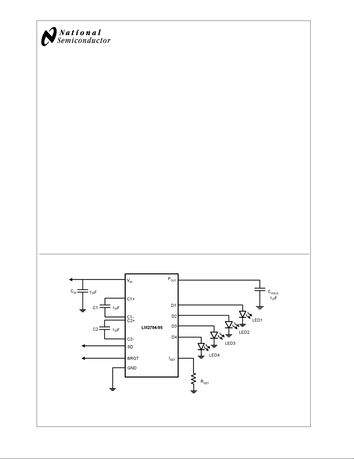
Basic Application Circuit
20028503
© 2004 National Semiconductor Corporation DS200285 www.national.com
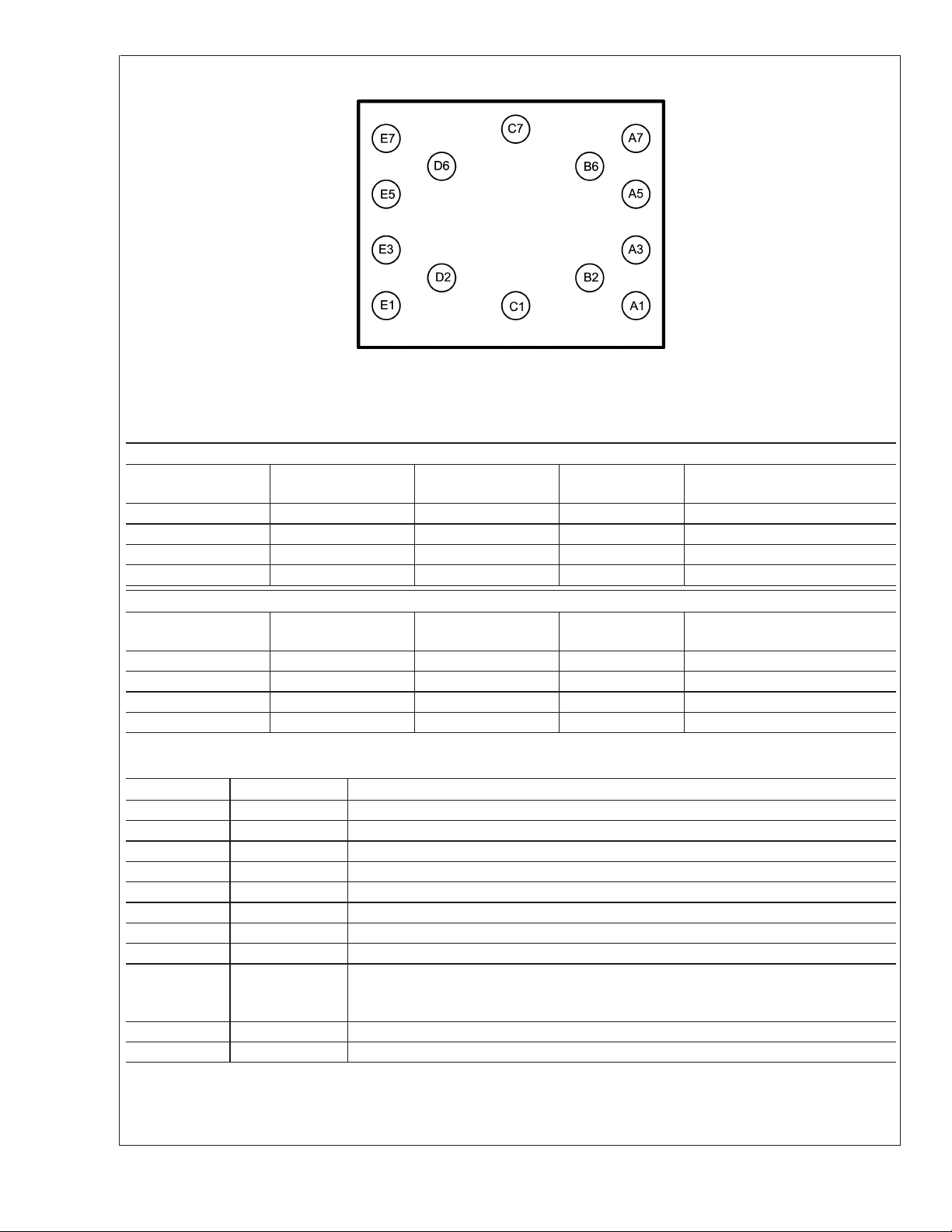
Connection Diagram
LM2794/LM2795
Bottom View
20028523
Ordering Information
Standard Micro SMD Package:
Order Number Shutdown Polarity Package Number Package
Supplied As
Marking
LM2794BL Active Low BLP14EHB I LOG 250 Units, Tape and Reel
LM2794BLX Active Low BLP14EHB I LOG 3000 Units, Tape and Reel
LM2795BL Active High BLP14EHB I LOJ 250 Units, Tape and Reel
LM2795BLX Active High BLP14EHB I LOJ 3000 Units, Tape and Reel
Thin Micro SMD Package:
Order Number Shutdown Polarity Package Number Package
Supplied As
Marking
LM2794TL Active Low TLP14EHA I LOG 250 Units, Tape and Reel
LM2794TLX Active Low TLP14EHA I LOG 3000 Units, Tape and Reel
LM2795TL Active High TLP14EHA I LOJ 250 Units, Tape and Reel
LM2795TLX Active High TLP14EHA I LOJ 3000 Units, Tape and Reel
Pin Description
Pin(*) Name Function
A1 C1+ Positive terminal of C1
B2 C1− Negative terminal of C1
C1 V
IN
D2 GND Power supply ground input
E1 C2− Negative terminal of C2
E3,E5,E7,D6 D1−4 Current source outputs. Connect directly to LED
C7 I
SET
B6 BRGT Variable voltage input controls output current
A7 SD The LM2794 has an active-low shutdown pin (LOW = shutdown, HIGH = operating). The
A5 C2+ Positive terminal of C2
A3 P
(*) Note that the pin numbering scheme for the Micro SMD package was revised in April, 2002 to conform to JEDEC standard. Only the pin numbers were revised.
No changes to the physical location of the inputs/outputs were made. For reference purpose, the obsolete numbering had C1+ as pin 1, C1- as pin 2, VIN as pin
3, GND as pin 4, C2- as pin 5, D1-D4 as pin 6,7,8 & 9, Iset as pin 10, BRGT as pin 11, SD as pin 12, C2+ as pin 13, Pout as pin 14
OUT
Power supply voltage input
Current Sense Input. Connect 1% resistor to ground to set constant current through LED
LM2795 has an active-high shutdown pin (HIGH = shutdown, LOW = operating) that has a
pull-up to V
.
IN
Charge pump output
www.national.com 2

LM2794/LM2795
Absolute Maximum Ratings (Note 1)
If Military/Aerospace specified devices are required,
please contact the National Semiconductor Sales Office/
Distributors for availability and specifications.
V
IN
SD −0.5 to (V
−0.5 to 6.2V max
+0.3V) w/
IN
θ
(Notes 2, 3) 125˚C/W
JA
Storge Temperature −65˚C to +150˚C
Lead Temp. (Soldering, 5 sec.) 260˚C
ESD Rating (Note 4)
Human Body Model 2kV
Machine Model 200V
6.2V max
BRGT −0.5 to (V
Continuous Power Dissipation
(Note 2) Internally Limited
(Note 2) 135˚C
T
JMAX
+0.3V) w/
IN
6.2V max
Operating Conditions
Input Voltage (VIN) 2.7V to 5.5V
Ambient Temperature (T
Junction Temperature (T
) −30˚C to +85˚C
A
) −30˚C to +100˚C
J
Electrical Characteristics
Limits in standard typeface are for TJ= 25˚C and limits in boldface type apply over the full Operating Junction Temperature
Range (−30˚C ≤ T
≤ +100˚C). Unless otherwise specified, C1 = C2 = CIN=C
J
=124Ω ; LM2794:VSD=VIN(LM2795: VSD= 0V).
Symbol Parameter Conditions Min Typ Max Units
I
DX
Available Current at Output Dx 3.0V ≤ VIN≤ 5.5V
≤ 3.8V
V
DX
BRGT = 50mV
2.7V ≤ V
V
DX
IN
≤ 3.6V
≤ 3.0V
BRGT = 0V
≤ 3.8V
V
DX
BRGT = 200mV
V
DX
Available Voltage at Output Dx 3.0V ≤ VIN≤ 5.5V
≤ 15mA
I
DX
BRGT = 50mV
I
DX
I
DX
I
D-MATCH
Line Regulation of Dx Output
Current
Load Regulation of Dx Output
Current
Current Matching Between Any
3.0V ≤ VIN≤ 5.5V
= 3.6V
V
DX
3.0V ≤ V
V
DX
IN
= 3.6V
≤ 4.4V
VIN= 3.6V
3.0V ≤ V
DX
≤ 3.8V
VIN= 3.6V, VDX= 3.6V 0.5 %
Two Outputs
I
Q
Quiescent Supply Current 3.0V ≤ VIN≤ 4.2V, Active, No
Load Current
= OPEN
R
SET
I
SD
I
PULL-SD
Shutdown Supply Current 3.0V ≤ VIN≤ 5.5V, Shutdown 2.3 5 µA
Shutdown Pull-Up Current
VIN= 3.6V 1.5 µA
(LM2795)
V
CP
Input Charge-Pump Mode To
Pass Mode Threshold
V
CPH
Input Charge-Pump Mode To
(Note 5) 250 mV
Pass Mode Hysteresis
V
IH
SD Input Logic High (LM2794) 3.0V ≤ VIN≤ 5.5V 1.0 V
SD Input Logic High (LM2795) 0.8V
V
IL
SD Input Logic Low (LM2794) 3.0V ≤ VIN≤ 5.5V 0.2 V
SD Input Logic Low (LM2795) 0.2V
I
LEAK-SD
R
BRGT
I
SET
SD Input Leakage Current 0V ≤ VSD≤ V
IN
BRGT Input Resistance 240 kΩ
I
Pin Output Current IDX/10 mA
SET
= 1 µF, VIN= 3.6V, BRGT pin = 0V; R
HOLD
15 16.8 mA
10
20
3.8 V
14.18 15.25 16.78 mA
14.18 15.25 16.32 mA
14.18 15.25 16.32 mA
5.5 8.2 mA
4.7 V
IN
100 nA
IN
SET
mA
mA
www.national.com3
Electrical Characteristics (Continued)
Limits in standard typeface are for TJ= 25˚C and limits in boldface type apply over the full Operating Junction Temperature
Range (−30˚C ≤ T
≤ +100˚C). Unless otherwise specified, C1 = C2 = CIN=C
J
=124Ω ; LM2794:VSD=VIN(LM2795: VSD= 0V).
Symbol Parameter Conditions Min Typ Max Units
LM2794/LM2795
f
SW
Note 1: Absolute maximum ratings indicate limits beyond which damage to the device may occur. Electrical specifications do not apply when operating the device
beyond its rated operating conditions.
Note 2: Internal thermal shutdown circuitry protects the device from permanent damage. Thermal shutdown engages at T
T
=140˚C (typ.). D1, D2, D3 and D4 may be shorted to GND without damage. P
J
Note 3: The value of θ
Note 4: In the test circuit, all capacitors are 1.0µF, 0.3Ω maximum ESR capacitors. Capacitors with higher ESR will increase output resistance, reduce output
voltage and efficiency.
Note 5: Voltage at which the device switches from charge-pump mode to pass mode or pass mode to charge-pump mode. For example, during pass mode the
device output (Pout) follows the input voltage.
Note 6: The output switches operate at one eigth of the oscillator frequency, f
Switching Frequency (Note 6) 3.0V ≤ VIN≤ 4.4V 325 515 675 kHz
may be shorted to GND for 1sec without damage.
is based on a two layer evaluation board with a dimension of 2in. x1.5in.
JA
OUT
OSC
= 1/8fSW.
= 1 µF, VIN= 3.6V, BRGT pin = 0V; R
HOLD
=150˚C (typ.) and disengages at
J
SET
www.national.com 4
LM2794/LM2795
Typical Performance Characteristics Unless otherwise specified, C1 = C2 = C
= 3.6V, BRGT pin = 0V, R
V
IN
I
DIODE
I
DIODE
BRGT = 3V I
SET
vs V
vs V
= 124Ω.
IN
IN
20028512
I
DIODE
DIODE
vs BRGT
vs R
SET
IN=CHOLD
20028509
= 1µF,
I
DIODE
V
20028507
vs R
SET
=0V I
BRGT
20028541
DIODE
vs V
20028508
DIODE
20028524
www.national.com5
 Loading...