

LM2771
Low-Ripple 250mA Switched Capacitor Step-Down
DC/DC Converter
LM2771 Low-Ripple 250mA Switched Capacitor Step-Down DC/DC Converter
March 2006
General Description
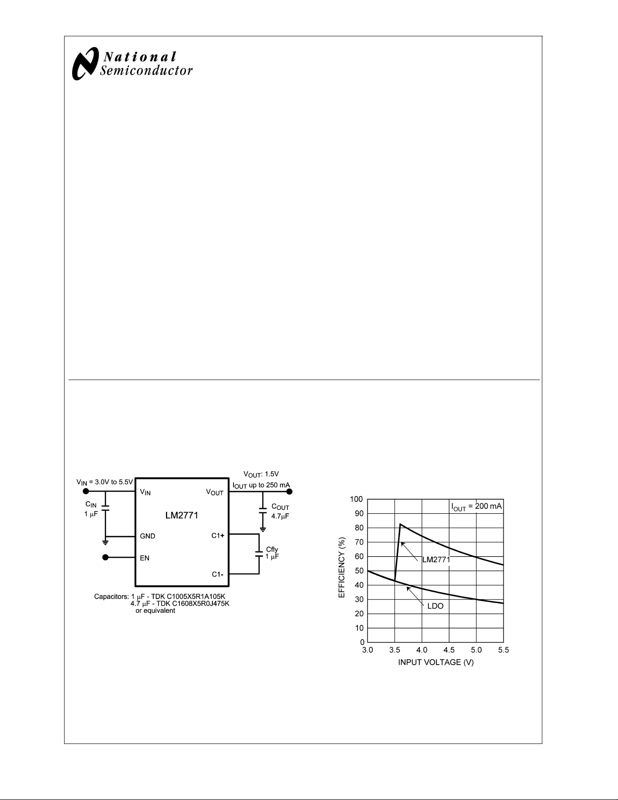
The LM2771 is a switched capacitor step-down regulator
that produces a 1.5V output without the use of an inductor. It
is capable of supplying loads up to 250mA. The LM2771
operates with an input voltage from 2.7V to 5.5V, and requires only 3 low-cost ceramic capacitors.
The LM2771 uses a regulated 0.5x charge pump to give
power conversion efficiencies nearly twice as high as an
LDO. Pre-regulated 1.1MHz fixed-frequency switching results in very low ripple and noise on both the input and the
output. When output currents are low (
automatically switches to a low-ripple PFM regulation mode
to maintain high efficiency over the entire load range. At
input voltages below 3.5V (Typ), the charge pump goes into
pass mode, with efficiencies similar to an LDO.
The LM2771 is available in National’s 10-pad Leadless
Leadframe No-Pullback Package (LLP-10).
<
30mA typ.), the part
Typical Application Circuit
Features
n Low-Noise Fixed Frequency Operation
n 1.5V Output Voltage
n Li-Ion (3.6V) to 1.5V with 81% Efficiency
n 1.7% Output Voltage Accuracy
n Very Low Output Ripple: 8mV
n Output Currents up to 250mA
n 2.7V to 5.5V Input Range
n Shutdown Disconnects Load from V
n 1.1MHz Switching Frequency
n No Inductors…Small Solution Size
n Current Limit and Thermal Protection
n LLP-10 Package (3mm x 3mm x 0.8mm)
@
250mA
IN
Applications
n DSP, Memory, and Microprocessor Power Supplies
n Mobile Phones and Pagers
n Portable Electronic Devices
LM2771 Efficiency vs.
Low-Dropout Linear Regulator (LDO) Efficiency
20183801
20183813
© 2006 National Semiconductor Corporation DS201838 www.national.com
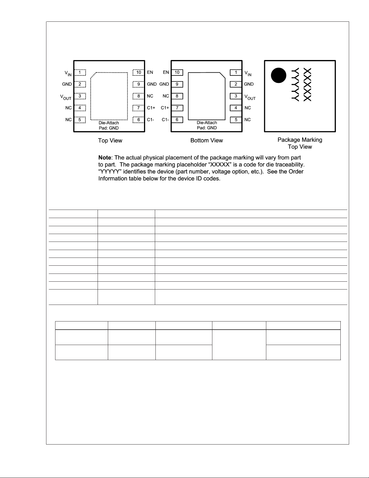
Connection Diagram and Package Mark Information
LM2771
10-Pin Non-Pullback Leadless Frame Package (LLP-10)
National Semiconductor Package Number SDA10A
Pin Descriptions
20183802
Pin # Name Description
1V
2 GND Ground
3V
4 NC No Connect
5 NC No Connect
6 C1- Flying Capacitor 1: Negative Terminal
7 C1+ Flying Capacitor 1: Positive Terminal
8 NC No Connect
9 GND Ground
10 EN Enable Pin Logic Input. Applying a logic HIGH voltage signal enables the part.
IN
OUT
Input Voltage: Recommended VINoperating range 3.0V to 5.5V.
Output Voltage
A logic LOW voltage signal places the the device in shutdown.
Order Information
Output Voltages Order Number Package Mark ID Package Supplied as:
1.5V LM2771SD XXXXX = CZC2CX
YYYYY = L2771
1.5V LM2771SDX XXXXX = CZC2CX
YYYYY = L2771
SDA10A
Non-Pullback LLP
1000 Units, Tape and Reel
4500 Units, Tape and Reel
www.national.com 2
LM2771
Absolute Maximum Ratings (Notes 1, 2)
If Military/Aerospace specified devices are required,
please contact the National Semiconductor Sales Office/
Distributors for availability and specifications.
Pin Voltage -0.3V to 6.0V
V
IN
EN Pin Voltage -0.3V to (V
Continuous Power Dissipation
Internally Limited
(Note 3)
Junction Temperature (T
) 150oC
J-MAX
Storage Temperature Range -65
Maximum Lead Temperature
+0.3V)
IN
w/ 6.0V max
o
C to +150oC
265
o
C
Operating Ratings (Notes 1, 2)
Input Voltage Range 2.7V to 5.5V
Recommended Load Current Range 0mA to 250mA
Junction Temperature (T
Ambient Temperature (T
) Range -30˚C to +110˚C
J
) Range
A
-30˚C to +85˚C
(Note 6)
Thermal Properties
Junction-to-Ambient Thermal
Resistance (θ
), LLP10 Package
JA
(Note 7)
55˚C/W
(Note 4)
ESD Rating (Note 5)
Human Body Model:
Machine Model
2.0kV
200V
Electrical Characteristics (Notes 2, 8)
Limits in standard typeface are for TJ=25oC. Limits in boldface type apply over the full operating junction temperature range
(-30˚C ≤ T
= 3.6V; V(EN) = 1.8V, CIN=C1= 1.0µF, C
Symbol Parameter Condition Min Typ Max Units
V
OUT
V
OUT/IOUT
V
OUT/VIN
E Power Efficiency I
I
Q
V
R
V
R–PFM
I
SD
F
SW
R
OL
I
CL
t
ON
V
IL
V
IH
I
IH
I
IL
Note 1: Absolute Maximum Ratings indicate limits beyond which damage to the component may occur. Operating Ratings are conditions under which operation of
the device is guaranteed. Operating Ratings do not imply guaranteed performance limits. For guaranteed performance limits and associated test conditions, see the
Electrical Characteristics tables.
Note 2: All voltages are with respect to the potential at the GND pins.
Note 3: Internal thermal shutdown circuitry protects the device from permanent damage. Thermal shutdown engages at T
T
=140oC (typ.).
J
≤ +110˚C) . Unless otherwise noted, specifications apply to the LM2771 Typical Application Circuit (pg. 1) with: V
J
1.5V Output Voltage Regulation 3.0V ≤ VIN≤ 5.5V
Output Load Regulation V
= 4.7µF. (Note 9)
OUT
0mA ≤ I
3.0V ≤ V
I
3.0V
0mA ≤ I
0mA ≤ I
OUT
OUT
OUT
IN
= 150mA
<
VIN≤ 5.5V,
OUT
= 1.5V
OUT
≤ 200mA
≤ 5.5V
≤ 250mA
≤ 250mA
1.455
(−3%)
1.475
(−1.7%)
1.445
(−3.7%)
1.5 1.545
(+3%)
1.5 1.525
(+1.7%)
1.5 1.545
(+3%)
0.17 mV/mA
Output Line Regulation 0.1 %/V
= 200mA 81 %
OUT
Quiescent Supply Current I
OUT
= 0mA
45 50 µA
(Note 10)
Fixed Frequency Output Ripple 40mA ≤ I
PFM–Mode Output Ripple I
OUT
<
≤ 250mA 8 mV
OUT
40mA 12 mV
Shutdown Current V(EN) = 0V 0.1 0.5 µA
Switching Frequency 3.2V ≤ VIN≤ 5.5V 0.80 1.1 1.40 MHz
Open–Loop Output Resistance I
OUT
= 200mA
1.0 Ω
(Note 11)
Output Current Limit VIN= 5.5V
0V ≤ V
OUT
≤ 0.2V
500 mA
(Note 12)
Turn-on Time 150 µs
Logic-low Input Voltage 3.0V ≤ VIN≤ 5.5V 0 0.5 V
Logic-high Input Voltage 3.0V ≤ VIN≤ 5.5V 0.95 V
Logic-high Input Current V(EN) = 1.8V
5µA
IN
(Note 13)
Logic-low Input Current Logic Input = 0V 0.1 µA
=150oC (typ.) and disengages at
J
IN
V
V
www.national.com3
 Loading...