

查询LM2766M6供应商
LM2766
Switched Capacitor Voltage Converter
LM2766 Switched Capacitor Voltage Converter
March 2000
General Description
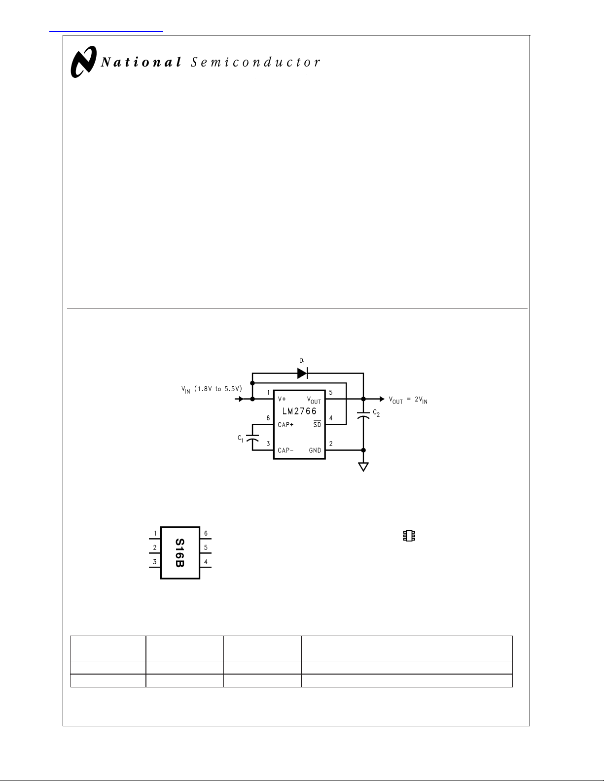
The LM2766 CMOS charge-pump voltage converter operates as a voltage doubler for an input voltage in the range of
+1.8V to +5.5V. Two low cost capacitors and a diode are
used in this circuit to provide up to 20 mAof output current.
The LM2766 operates at 200 kHz switching frequency to reduce output resistance and voltage ripple. With an operating
current of only350 µA (operating efficiency greater than 90%
with most loads) and 0.1µA typical shutdown current, the
LM2766 provides ideal performance for battery powered
systems. The device is manufactured in a SOT-23-6 package.
Basic Application Circuits
Voltage Doubler
Features
n Doubles Input Supply Voltage
n SOT23-6 Package
n 20Ω Typical Output Impedance
n 90% Typical Conversion Efficiency at 20 mA
n 0.1µA Typical Shutdown Current
Applications
n Cellular Phones
n Pagers
n PDAs
n Operational Amplifier Power Supplies
n Interface Power Supplies
n Handheld Instruments
DS101282-1
Connection Diagram
6-Lead SOT (M6)
DS101282-22
Actual Size
DS101282-13
Top View With Package Marking
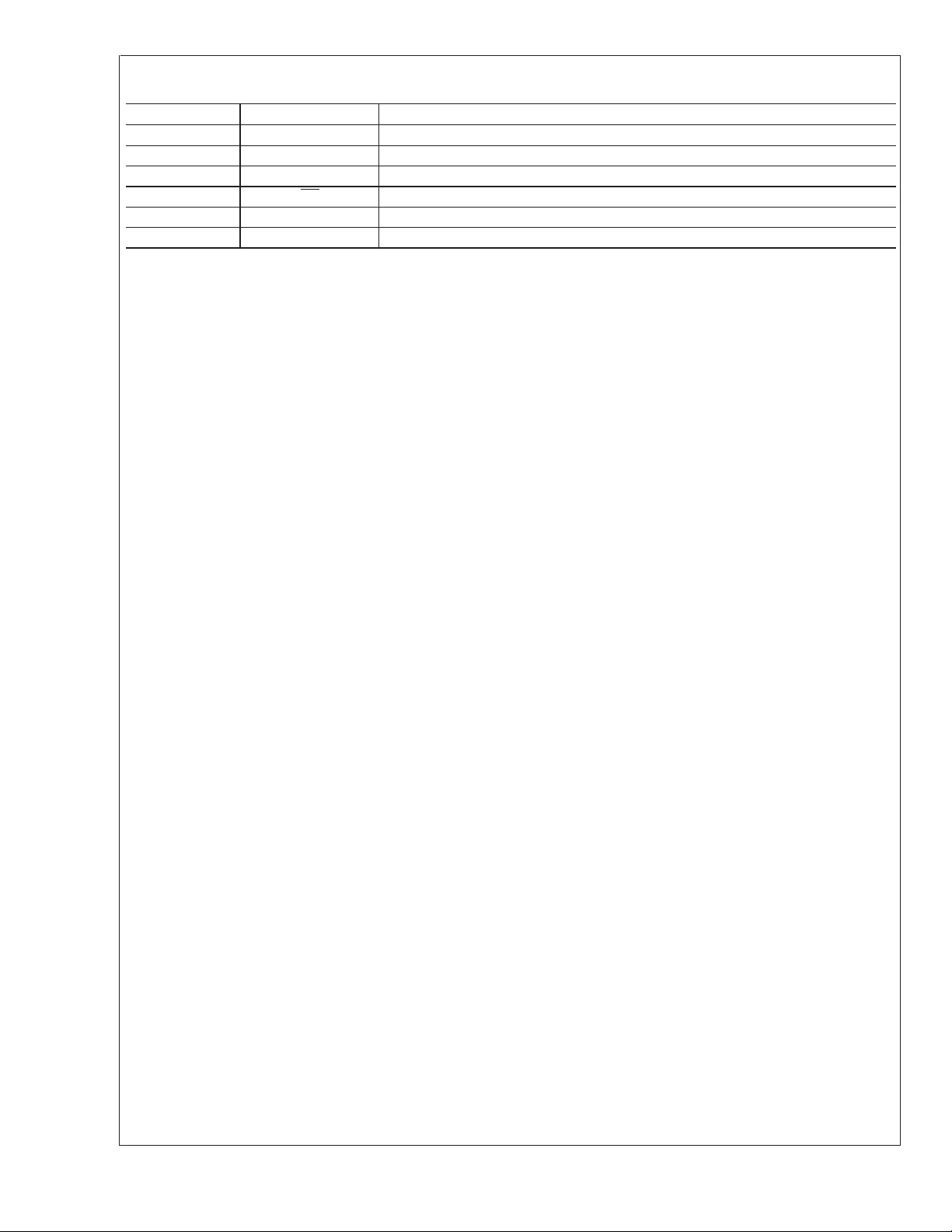
Ordering Information
Order Number Package
Number
LM2766M6 MA06A S16B (Note 1) Tape and Reel (1000 units/reel)
LM2766M6X MA06A S16B (Note 1) Tape and Reel (3000 units/reel)
Note 1: The small physical size of the SOT-23 package does not allow for the full part number marking. Devices will be marked with the designation shown in
the column Package Marking.
© 2000 National Semiconductor Corporation DS101282 www.national.com
Package
Marking
Supplied as
Pin Description
LM2766
Pin Name Function
1 V+ Power supply positive voltage input.
2 GND Power supply ground input.
3 CAP− Connect this pin to the negative terminal of the charge-pump capacitor.
4SD
5V
6 CAP+ Connect this pin to the positive terminal of the charge-pump capacitor.
OUT
Shutdown control pin, tie this pin to V+ in normal operation.
Positive voltage output.
www.national.com 2
Absolute Maximum Ratings (Note 2)
If Military/Aerospace specified devices are required,
please contact the National Semiconductor Sales Office/
Distributors for availability and specifications.
Supply Voltage (V+ to GND, or V+ to V
SD
(GND − 0.3V) to (V+ +
) 5.8V
OUT
0.3V)
V
Continuous Output Current 40 mA
OUT
Output Short-Circuit Duration to GND (Note 3) 1 sec.
Continuous Power
Dissipation (T
T
(Note 4) 150˚C
JMax
= 25˚C)(Note 4)
A
600 mW
Operating Ratings
θJA(Note 4) 210˚C/W
Junction Temperature Range −40˚ to 100˚C
Ambient Temperature Range −40˚ to 85˚C
Storage Temperature Range −65˚C to 150˚C
Lead Temp. (Soldering, 10
seconds) 240˚C
ESD Rating (Note 5)
Human body model
Machine model
200V
2kV
Electrical Characteristics
Limits in standard typeface are for TJ= 25˚C, and limits in boldface type apply over the full operating temperature range. Unless otherwise specified: V+ = 5V, C
Symbol Parameter Condition Min Typ Max Units
V+ Supply Voltage 1.8 5.5 V
I
Q
I
SD
V
SD
I
L
R
OUT
f
OSC
f
SW
P
EFF
V
OEFF
Note 2: Absolute maximum ratings indicate limits beyond which damage to the device may occur. Electrical specifications do not apply when operating the device
beyond its rated operating conditions.
Note 3: V
peratures above 85˚C, V
Note 4: The maximum allowable power dissipation is calculated by using P
ambient temperature, and θ
Note 5: The human body model is a 100pF capacitor discharged through a 1.5kΩ resistor into each pin. The machine model is a 200pF capacitor discharged directly
into each pin.
Note 6: In the test circuit, capacitors C
voltage and efficiency.
Note 7: Specified output resistance includes internal switch resistance and capacitor ESR. See the details in the application information for positive voltage doubler.
Note 8: The output switches operate at one half of the oscillator frequency, f
Supply Current No Load 350 950 µA
Shutdown Supply Current 0.1 0.5
Shutdown Pin Input Voltage Shutdown Mode 0.6
Output Current 2.5V ≤ VIN≤ 5.5V 20
Output Resistance (Note 7) IL=20mA 20 55 Ω
Oscillator Frequency (Note 8) 220 400 700 kHz
Switching Frequency (Note 8) 110 200 350 kHz
Power Efficiency IL= 20 mA to GND 94 %
Voltage Conversion Efficiency No Load 99.96 %
may be shorted to GND for one second without damage. However, shorting V
OUT
must not be shorted to GND or V+, or device may be damaged.
OUT
is the junction-to-ambient thermal resistance of the specified package.
JA
and C2are 1.0 µF, 0.3Ω maximum ESR capacitors. Capacitors with higher ESR will increase output resistance, reduce output
1
= 1.0 µF. (Note 6)
1=C2
= 85˚C 0.2
T
A
Normal Operation 2.0
<
1.8V ≤ V
2.5V 10
IN
to V+ may damage the device and should be avoided. Also, for tem-
OUT
DMax
OSC
=(T
=2fSW.
JMax−TA
)/θJA, where T
is the maximum junction temperature, TAis the
JMax
mA
LM2766
µA
V
www.national.com3
 Loading...