

December 5, 2007
LM2756
Multi-Display Inductorless LED Driver with 32 Exponential
Dimming Steps in micro SMD
LM2756 Multi-Display Inductorless LED Driver with 32 Exponential Dimming Steps in micro SMD
General Description
The LM2756 is a highly integrated, switched-capacitor, multidisplay LED driver that can drive up to 8 LEDs in parallel with
a total output current of 180mA. Regulated internal current
sources deliver excellent current and brightness matching in
all LEDs.
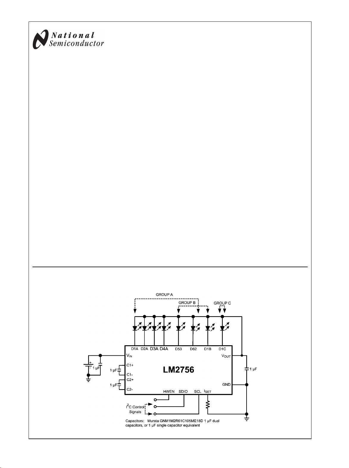
The LED driver current sinks are split into three independently
controlled groups. The primary group (Group A) can be configured to drive four, five or six LEDs for use in the main phone
display, while the secondary group (Group B) can be configured to drive one, two or three LEDs for driving secondary
displays, keypads and/or indicator LEDs. An additional driver,
D1C, is provided for additional indicator lighting functions.
The device provides excellent efficiency without the use of an
inductor by operating the charge pump in a gain of 3/2 or in
Pass-Mode. The proper gain for maintaining current regulation is chosen, based on LED forward voltage, so that efficiency is maximized over the input voltage range.
The LM2756 is available in National’s tiny 20-bump, 0.4mm
pitch, thin micro SMD package.
Features
Drives up to 8 LEDs with up to 30mA of Diode Current
■
Each
32 Exponential Dimming Steps with 800:1 Dimming Ratio
■
for Group A (Up to 6 LEDs)
8 Linear Dimming States for Groups B (Up to 3 LEDs) and
■
D1C (1 LED)
Programmable Auto-Dimming Function
■
3 Independently Controlled LED Groups Via I2C
■
Compatible Interface
Up to 90% Efficiency
■
Total Solution Size < 21mm
■
Low Profile 20 Bump micro SMD Package
■
(1.615mm × 2.015mm × 0.6mm)
0.4% Accurate Current Matching
■
Internal Soft-Start Limits Inrush Current
■
True Shutdown Isolation for LED’s
■
Wide Input Voltage Range (2.7V to 5.5V)
■
Active High Hardware Enable
■
2
Applications
Dual Display LCD Backlighting for Portable Applications
■
Large Format LCD Backlighting
■
Display Backlighting with Indicator Light
■
Typical Application Circuit
30009701
© 2007 National Semiconductor Corporation 300097 www.national.com

LM2756
Minimum Layout
30009741
Connection Diagram
20 Bump micro SMD Package
NS Package Number TMD20AAA
30009702
Pin Descriptions
Bump #s
TMD20AAA
A3 V
A2 V
A1, C1, B1, B2 C1+, C1-, C2+, C2- Flying Capacitor Connections
D3, E3,E4, D4 D1A-D4A LED Drivers - GroupA
C4, B4 D53, D62 LED Drivers - Configurable Current Sinks. Can be assigned to GroupA or GroupB
B3 D1B LED Drivers - GroupB
C3 D1C LED Driver - Indicator LED
D2 I
E1 HWEN Hardware Enable Pin. High = Normal Operation, Low = RESET
C2 SDIO Serial Data Input/Output Pin
E2 SCL Serial Clock Pin
A4, D1 GND Ground
Pin Names Pin Descriptions
IN
OUT
SET
Input voltage. Input range: 2.7V to 5.5V.
Charge Pump Output Voltage
Placing a resistor (R
) between this pin and GND sets the full-scale LED current for
SET
DxA , DxB, D53, D62 and D1C LEDs.
Full-Scale LED Current = 189 × (1.25V ÷ R
SET
)
Ordering Information
Order Information Package Supplied As
LM2756TM
LM2756TMX 3000 Units, Tape & Reel
www.national.com 2
TMD20AAA
250 Units, Tape & Reel
LM2756
Absolute Maximum Ratings (Notes 1, 2)
If Military/Aerospace specified devices are required,
please contact the National Semiconductor Sales Office/
Distributors for availability and specifications.
VIN pin voltage -0.3V to 6.0V
SCL, SDIO, HWEN pin voltages -0.3V to (VIN+0.3V)
w/ 6.0V max
I
Pin Voltages -0.3V to (V
Dxx
Continuous Power Dissipation
Internally Limited
(Note 3)
Junction Temperature (T
) 150°C
J-MAX
Storage Temperature Range -65°C to +150° C
Maximum Lead Temperature
(Soldering)
ESD Rating(Note 5)
Human Body Model 2.0kV
+0.3V)
VOUT
w/ 6.0V max
(Note 4)
Operating Rating
(Notes 1, 2)
Input Voltage Range 2.7V to 5.5V
LED Voltage Range 2.0V to 4.0V
Junction Temperature (TJ) Range
Ambient Temperature (TA) Range
(Note 6)
-30°C to +105°C
-30°C to +85°C
Thermal Properties
Junction-to-Ambient Thermal
Resistance (θJA),
TMD20 Package
40°C/W
(Note 7)
ESD Caution Notice National Semiconductor
recommends that all integrated circuits be handled with
appropriate ESD precautions. Failure to observe proper ESD
handling techniques can result in damage to the device.
Electrical Characteristics (Notes 2, 8)
Limits in standard typeface are for TJ = 25°C, and limits in boldface type apply over the full operating temperature range. Unless
otherwise specified: VIN = 3.6V; V
Current; ENA, ENB, ENC Bits = “1”; SD53, SD62, 53A, 62A Bits = "0"; C1 = C2 = CIN= C
output current(s) and current setting pins (I
Symbol Parameter Condition Min Typ Max Units
Output Current Regulation
GroupA
Output Current Regulation
GroupB
I
Dxx
Output Current Regulation
IDC
Maximum Diode Current per Dxx
Output(Note 10)
Output Current Regulation
GroupA, GroupB, and GroupC
Enabled
(Note 10)
I
Dxx-
MATCH
V
DxTH
LED Current Matching(Note 11)
V
1x to 3/2x Gain Transition
Dxx
Threshold
Current sink Headroom Voltage
V
HR
Requirement
(Note 12)
R
OUT
I
Q
Open-Loop Charge Pump Output
Resistance
Quiescent Supply Current Gain = 1.5x, No Load 2.1 2.5 mA
HWEN
= VIN; V
Dxx
= V
= V
DxA
and I
DxB
) apply to GroupA and GroupB. (Note 9)
SET
= 0.4V; R
DxC
2.7V ≤ VIN ≤ 5.5V
ENA = '1', 53A = 62A = '0'', ENB = ENC = '0'
4 LEDs in GroupA
2.7V ≤ VIN ≤ 5.5V
ENA = '1', 53A = 62A = '1', ENB = ENC = '0'
6 LEDs in GroupA
2.7V ≤ VIN ≤ 5.5V
ENB = '1', 53A = 62A = '0', ENA = ENC = '0'
3 LEDs in GroupB
2.7V ≤ VIN ≤ 5.5V
ENC = '1', ENA = ENB = '0'
R
= 8.33kΩ
SET
3.2V ≤ VIN ≤ 5.5V
V
= 3.6V
LED
R
= 10.5kΩ
SET
= 11.8kΩ; GroupA = GroupB = GroupC = Fullscale
SET
= 1.0µF; Specifications related to
OUT
18.65
(-8%)
18.70
(-8.5%)
18.40
(-8%)
18.20
(-7.5%)
20.28
20.40
20.00
19.70
30 mA
22.5
DxA
22.5
DxB
22.5
DxC
GroupA (4 LEDs) 0.4 1.8
2.7V ≤ VIN ≤ 5.5V
GroupB (3 LEDs) 0.7 2.5
V
and/or V
DxA
I
= 95% ×I
Dxx
(I
(nom) ≈ 20mA)
Dxx
DxB
Dxx
Falling
(nom.)
150 mV
65 mV
Gain = 3/2 2.4
Gain = 1 0.9
21.90
(+8%)mA(%)
22.10
(+8.5%)mA(%)
21.60
(+8%)mA(%)
21.20
(+7.5%)mA(%)
mA
%GroupA (6 LEDs) 1.0 2.7
Ω
3 www.national.com
Symbol Parameter Condition Min Typ Max Units
I
SD
LM2756
V
SET
I
DxA-B-C /
I
SET
f
SW
t
START
V
HWEN
Shutdown Supply Current All ENx bits = "0" 3.7 5.5 µA
I
Pin Voltage
SET
Output Current to Current Set Ratio
GroupA, GroupB, GroupC
2.7V ≤ VIN ≤ 5.5V
189
1.25 V
Switching Frequency 1.0 1.3 1.6 MHz
V
Start-up Time
HWEN Voltage Thresholds
= 90% steady state
OUT
2.7V ≤ VIN ≤ 5.5V
250 µs
Reset 0 0.580
Normal Operation 1.075
V
IN
I2C Compatible Interface Voltage Specifications (SCL, SDIO)
V
IL
V
IH
V
OL
Input Logic Low "0"
Input Logic High "1"
Output Logic Low "0"
2.7V ≤ VIN ≤ 5.5V
2.7V ≤ VIN ≤ 5.5V
I
= 3.5mA
LOAD
0 0.710 V
1.225
V
IN
400 mV
I2C Compatible Interface Timing Specifications (SCL, SDIO)(Note 13)
t
1
t
2
t
3
t
4
t
5
SCL (Clock Period) (Note 14) 294 ns
Data In Setup Time to SCL High 100 ns
Data Out stable After SCL Low 0 ns
SDIO Low Setup Time to SCL Low
(Start)
SDIO High Hold Time After SCL High
(Stop)
100 ns
100 ns
V
V
30009713
Note 1: Absolute Maximum Ratings indicate limits beyond which damage to the component may occur. Operating Ratings are conditions under which operation
of the device is guaranteed. Operating Ratings do not imply guaranteed performance limits. For guaranteed performance limits and associated test conditions,
see the Electrical Characteristics tables.
Note 2: All voltages are with respect to the potential at the GND pins.
Note 3: Internal thermal shutdown circuitry protects the device from permanent damage. Thermal shutdown engages at TJ = 160°C (typ.) and disengages at T
= 155°C (typ.).
Note 4: For detailed soldering specifications and information, please refer to National Semiconductor Application Note 1112: Micro SMD Wafer Level Chip Scale
Package (AN-1112).
Note 5: The human body model is a 100pF capacitor discharged through a 1.5kΩ resistor into each pin. (MIL-STD-883 3015.7)
Note 6: In applications where high power dissipation and/or poor package thermal resistance is present, the maximum ambient temperature may have to be
derated. Maximum ambient temperature (T
dissipation of the device in the application (P
following equation: T
Note 7: Junction-to-ambient thermal resistance is highly dependent on application and board layout. In applications where high maximum power dissipation
exists, special care must be paid to thermal dissipation issues in board design. For more information, please refer to National Semiconductor Application Note
1112: Micro SMD Wafer Level Chip Scale Package (AN-1112).
Note 8: Min and Max limits are guaranteed by design, test, or statistical analysis. Typical numbers are not guaranteed, but do represent the most likely norm.
Note 9: CIN, C
www.national.com 4
VOUT
= T
A-MAX
, C1, and C2 : Low-ESR Surface-Mount Ceramic Capacitors (MLCCs) used in setting electrical characteristics
J-MAX-OP
– (θJA × P
) is dependent on the maximum operating junction temperature (T
A-MAX
), and the junction-to ambient thermal resistance of the part/package in the application (θJA), as given by the
D-MAX
).
D-MAX
= 105°C), the maximum power
J-MAX-OP
J
Note 10: The maximum total output current for the LM2756 should be limited to 180mA. The total output current can be split among any of the three Groups
(I
= I
= I
DxA
proper current regulation. See the Maximum Output Current section of the datasheet for more information.
= 30mA Max.). Under maximum output current conditions, special attention must be given to input voltage and LED forward voltage to ensure
DxB
DxC
Note 11: For the two groups of current sinks on a part (GroupA and GroupB), the following are determined: the maximum sink current in the group (MAX), the
minimum sink current in the group (MIN), and the average sink current of the group (AVG). For each group, two matching numbers are calculated: (MAX-AVG)/
AVG and (AVG-MIN)/AVG. The largest number of the two (worst case) is considered the matching figure for the Group. The matching figure for a given part is
considered to be the highest matching figure of the two Groups. The typical specification provided is the most likely norm of the matching figure for all parts.
Note 12: For each Dxx pin, headroom voltage is the voltage across the internal current sink connected to that pin. For Group A, B, and C current sinks, V
V
-V
. If headroom voltage requirement is not met, LED current regulation will be compromised.
OUT
LED
HRx
=
Note 13: SCL and SDIO should be glitch-free in order for proper brightness control to be realized.
Note 14: SCL is tested with a 50% duty-cycle clock.
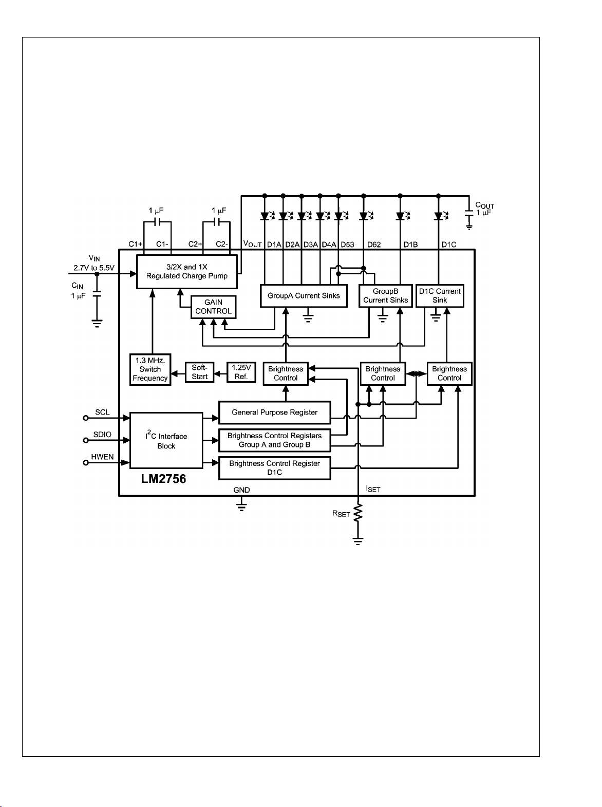
Block Diagram
LM2756
30009703
5 www.national.com

Typical Performance Characteristics Unless otherwise specified: T
V
LEDxA
LM2756
= V
LEDxB
= V
LED1C
= 3.6V; R
= 11.8kΩ; C1=C2= CIN = C
SET
LED Drive Efficiency vs Input Voltage
= 1µF; ENA = ENB = ENC = '1'.
VOUT
LED Drive Efficiency vs Input Voltage
= 25°C; VIN = 3.6V; V
A
HWEN
= VIN;
30009719
Input Current vs Input Voltage
30009720
GroupB Diode Current vs Input Voltage
30009721
GroupA Diode Current vs Input Voltage
30009726
GroupC Diode Current vs Input Voltage
30009727
www.national.com 6
30009728

LM2756
GroupA Current Matching vs Input Voltage
6 LEDs
30009716
GroupB Current Matching vs Input Voltage
3 LEDs
GroupA Current Matching vs Input Voltage
4 LEDs
30009717
GroupA Diode Current vs GroupA Brightness Code
30009718
GroupB Diode Current vs GroupB Brightness Code
30009723
30009722
GroupC Diode Current vs GroupC Brightness Code
30009724
7 www.national.com

LM2756
Quiescent Current in Gain 1.5× vs Input Voltage
Shutdown Current vs Input Voltage
30009714
30009715
www.national.com 8

LM2756
Circuit Description
OVERVIEW
The LM2756 is a white LED driver system based upon an
adaptive 3/2× - 1× CMOS charge pump capable of supplying
up to 180mA of total output current. With three separately
controlled Groups of constant current sinks, the LM2756 is an
ideal solution for platforms requiring a single white LED driver
for main display, sub display, and indicator lighting. The tightly
matched current sinks ensure uniform brightness from the
LEDs across the entire small-format display.
Each LED is configured in a common anode configuration,
with the peak drive current being programmed through the
use of an external R
is used to enable the device and vary the brightness within
the individual current sink Groups. For GroupA , 32 exponentially-spaced analog brightness control levels are available.
GroupB and GroupC have 8 linearly-spaced analog brightness levels.
CIRCUIT COMPONENTS
Charge Pump
The input to the 3/2× - 1× charge pump is connected to the
VIN pin, and the regulated output of the charge pump is connected to the V
range of the LM2756 is 2.7V to 5.5V. The device’s regulated
charge pump has both open loop and closed loop modes of
operation. When the device is in open loop, the voltage at
V
is equal to the gain times the voltage at the input. When
OUT
the device is in closed loop, the voltage at V
to 4.6V (typ.). The charge pump gain transitions are actively
selected to maintain regulation based on LED forward voltage
and load requirements.
LED Forward Voltage Monitoring
The LM2756 has the ability to switch gains (1x or 3/2x) based
on the forward voltage of the LED load. This ability to switch
gains maximizes efficiency for a given load. Forward voltage
monitoring occurs on all diode pins. At higher input voltages,
the LM2756 will operate in pass mode, allowing the V
voltage to track the input voltage. As the input voltage drops,
the voltage on the Dxx pins will also drop (V
V
). Once any of the active Dxx pins reaches a voltage
LEDx
approximately equal to 150mV, the charge pump will switch
to the gain of 3/2. This switch-over ensures that the current
through the LEDs never becomes pinched off due to a lack of
headroom across the current sinks. Once a gain transition
occurs, the LM2756 will remain in the gain of 3/2 until an
I2C write to the part occurs. At that time, the LM2756 will
re-evaluate the LED conditions and select the appropriate gain.
Only active Dxx pins will be monitored. For example, if only
GroupA is enabled, the LEDs in GroupB or GroupC will not
affect the gain transition point. If all 3 Groups are enabled, all
diodes will be monitored, and the gain transition will be based
upon the diode with the highest forward voltage.
Configurable Gain Transition Delay
To optimize efficiency, the LM2756 has a user selectable gain
transition delay that allows the part to ignore short duration
input voltage drops. By default, the LM2756 will not change
gains if the input voltage dip is shorter than 3 to 6 milliseconds.
There are four selectable gain transition delay ranges available on the LM2756. All delay ranges are set within the VF
Monitor Delay Register . Please refer to the INTERNAL REG-
resistor. An I2C compatible interface
SET
pin. The recommended input voltage
OUT
is regulated
OUT
= V
DXX
OUT
VOUT
ISTERS section of this datasheet for more information regarding the delay ranges.
HWEN Pin
The LM2756 has a hardware enable/reset pin (HWEN) that
allows the device to be disabled by an external controller
without requiring an I2C write command. Under normal operation, the HWEN pin should be held high (logic '1') to prevent
an unwanted reset. When the HWEN is driven low (logic '0'),
all internal control registers reset to the default states and the
part becomes disabled. Please see the Electrical Character-
istics section of the datasheet for required voltage thresholds.
I2C Compatible Interface
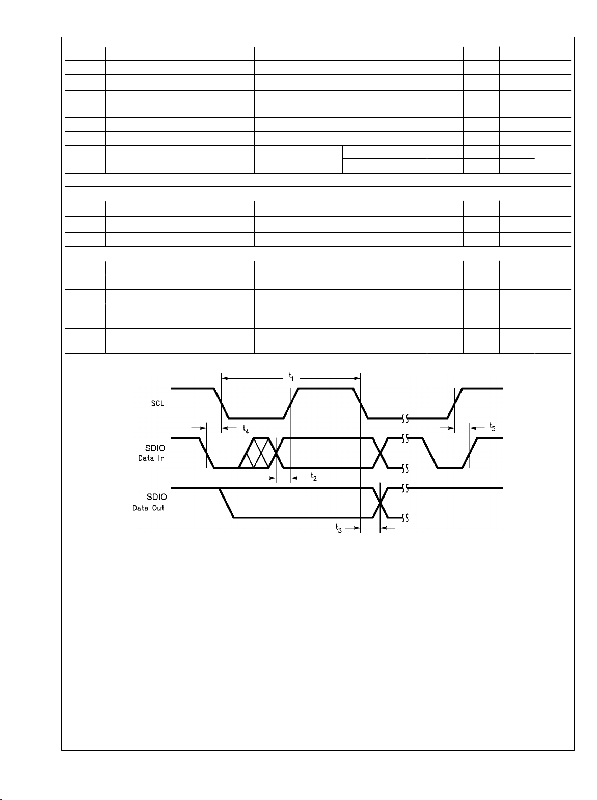
DATA VALIDITY
The data on SDIO line must be stable during the HIGH period
of the clock signal (SCL). In other words, state of the data line
can only be changed when SCL is LOW.
30009725
FIGURE 1. Data Validity Diagram
A pull-up resistor between the controller's VIO line and SDIO
must be greater than [ (VIO-VOL) / 3.5mA] to meet the V
requirement on SDIO. Using a larger pull-up resistor results
OL
in lower switching current with slower edges, while using a
smaller pull-up results in higher switching currents with faster
edges.
START AND STOP CONDITIONS
START and STOP conditions classify the beginning and the
end of the I2C session. A START condition is defined as SDIO
–
signal transitioning from HIGH to LOW while SCL line is
HIGH. A STOP condition is defined as the SDIO transitioning
from LOW to HIGH while SCL is HIGH. The I2C master always
generates START and STOP conditions. The I2C bus is considered to be busy after a START condition and free after a
STOP condition. During data transmission, the I2C master
can generate repeated START conditions. First START and
repeated START conditions are equivalent, function-wise.
30009711
FIGURE 2. Start and Stop Conditions
TRANSFERING DATA
Every byte put on the SDIO line must be eight bits long, with
the most significant bit (MSB) transferred first. Each byte of
data has to be followed by an acknowledge bit. The acknowledge related clock pulse is generated by the master. The
9 www.national.com

master releases the SDIO line (HIGH) during the acknowledge clock pulse. The LM2756 pulls down the SDIO line
during the 9th clock pulse, signifying an acknowledge. The
LM2756
LM2756 generates an acknowledge after each byte is received.
After the START condition, the I2C master sends a chip address. This address is seven bits long followed by an eighth
ack = acknowledge (SDIO pulled down by either master or slave)
id = chip address, 36h for LM2756
bit which is a data direction bit (R/W). The LM2756 address
is 36h. For the eighth bit, a “0” indicates a WRITE and a “1”
indicates a READ. The second byte selects the register to
which the data will be written. The third byte contains data to
write to the selected register.
30009712
FIGURE 3. Write Cycle
w = write (SDIO = "0")
r = read (SDIO = "1")
I2C COMPATIBLE CHIP ADDRESS
The chip address for LM2756 is 0110110, or 36h.
FIGURE 4. Chip Address
INTERNAL REGISTERS OF LM2756
Register Internal Hex
Power On Value
Address
General Purpose
10h 0000 0000
Register
Group A
A0h 1110 0000
Brightness Control
Register
Group B
B0h 1111 1000
Brightness Control
Register
Group C
C0h 1111 1000
Brightness Control
Register
Ramp Step Time
20h 1111 0000
Register
VF Monitor Delay
60h 1111 1100
Ragister
30009709
FIGURE 5. General Purpose Register Description
Internal Hex Address: 10h
Note:
ENA: Enables DxA LED drivers (Main Display)
ENB: Enables DxB LED drivers (Aux Lighting)
ENC: Enables D1C LED driver (Indicator Lighting)
SD53: Shuts down driver D53
SD62: Shuts down driver D62
53A: Configures D53 to GroupA
62A: Configures D62 to GroupA
FIGURE 6. Brightness Control Register Description
30009708
30009705
30009706
30009707
www.national.com 10

LM2756
Internal Hex Address: 0xA0 (GroupA), 0xB0 (GroupB),
0xC0 (GroupC)
Note:
DxA4-DxA0, D53, D62: Sets Brightness for DxA pins (GroupA).
11111=Fullscale
DxB2-DxB0: Sets Brightness for DxB pins (GroupB). 111=Fullscale
DxC2-DxC0: Sets Brightness for D1C pin. 111 = Fullscale
Full-Scale Current set externally by the following equation:
I
= 189 × 1.25V / R
Dxx
SET
Brightness Level Control Table (GroupA)
Brightness Code (hex) Perceived Brightness
Level (%)
00 0.125
01 0.313
02 0.625
03 1
04 1.125
05 1.313
06 1.688
07 2.063
08 2.438
09 2.813
0A 3.125
0B 3.75
0C 4.375
0D 5.25
0E 6.25
0F 7.5
10 8.75
11 10
12 12.5
13 15
14 16.875
15 18.75
16 22.5
17 26.25
18 31.25
19 37.5
1A 43.75
1B 52.5
1C 61.25
1D 70
1E 87.5
1F 100
GroupB and GroupC Brightness Levels (% of Full-Scale) =
10%, 20%, 30%, 40%, 50%, 60%, 70%, 100%
30009735
FIGURE 7. Ramp Step Time Register Description
Internal Hex Address: 20h
Note:
RS1-RS0: Sets Brightness Ramp Step Time. The Brightness ramp
settings only affect GroupA current sinks. ('00' = 100µs, '01' = 25ms,
'10' = 50ms, '11' = 100ms).
30009739
FIGURE 8. VF Monitor Delay Register Description
Internal Hex Address: 60h
Note:
VF1-VF0: Sets the Gain Transition Delay Time. The VF Monitor Delay
can be set to four different delay times. ('00' (Default) = 3-6msec., '01'
= 1.5-3msec., '10' = 0.4-0.8msec., '11' = 60-90µsec.).
Application Information
LED CONFIGURATIONS
The LM2756 has a total of 8 current sinks capable of sinking
180mA of total diode current. These 8 current sinks are configured to operate in three independently controlled lighting
regions. GroupA has four dedicated current sinks, while
GroupB and GroupC each have one. To add greater lighting
flexibility, the LM2756 has two additional drivers (D53 and
D62) that can be assigned to either GroupA or GroupB
through a setting in the general purpose register.
At start-up, the default condition is four LEDs in GroupA, three
LEDs in GroupB and a single LED in GroupC (NOTE: GroupC
only consists of a single current sink (D1C) under any configuration). Bits 53A and 62A in the general purpose register
control where current sinks D53 and D62 are assigned. By
writing a '1' to the 53A or 62A bits, D53 and D62 become assigned to the GroupA lighting region. Writing a '0' to these bits
assigns D53 and D62 to the GroupB lighting region. With this
added flexibility, the LM2756 is capable of supporting applications requiring 4, 5, or 6 LEDs for main display lighting,
while still providing additional current sinks that can be used
for a wide variety of lighting functions.
SETTING LED CURRENT
The current through the LEDs connected to DxA and DxB can
be set to a desired level simply by connecting an appropriately
sized resistor (R
GND. The DxA, DxB and D1C LED currents are proportional
to the current that flows out of the I
189 times greater than the I
of the internal amplifiers set the voltage of the I
(typ.). The statements above are simplified in the equations
below:
Once the desired R
has the ability to internally dim the LEDs using analog current
scaling. The analog current level is set through the I2C compatible interface. LEDs connected to GroupA can be dimmed
) between the I
SET
I
(A)= 189 × (V
DxA/B/C
R
(Ω)= 189 × (1.25V / I
SET
value has been chosen, the LM2756
SET
pin of the LM2756 and
SET
pin and are a factor of
SET
current. The feedback loops
SET
ISET
/ R
DxA/B/C
SET
SET
)
)
pin to 1.25V
11 www.national.com

to 32 different levels. GroupB and GroupC(D1C) have 8 analog current levels.
LM2756
Please refer to the I2C Compatible Interface section of this
datasheet for detailed instructions on how to adjust the brightness control registers.
LED CURRENT RAMPING
The LM2756 provides an internal LED current ramping function that allows the GroupA LEDs to turn on and turn off
gradually over time. The target current level is set in the
GroupA Brightness Control Register (0xA0). The total rampup/ramp-down time is determind by the GroupA brightness
level (0-31) and the user configurable ramp step time.
Bits RS1 and RS2 in the Ramp Step Time Register (0x20) set
the ramp step time to the following four times: '00' = 100µsec.,
'01' = 25msec., '10' = 50msec., '11' = 100msec.
The LM2756 will always ramp-up (upon enable) and rampdown (upon disable) through the brightness levels until the
target level is reached. At the default setting of '00', the
LM2756's current ramping feature looks more like a current
step rather than a current ramp. The following table gives the
approximate ramp-up/ramp-down times if the GroupA brightness register is set to full-scale, or brightness code 31.
Brightness Ramp-Up/Ramp-Down Times
Ramp Code
RS1-RS0
Ramp Step
Time
Total Ramp
Time
00 100µs 3.2ms
01 25ms 0.8s
10 50ms 1.6s
11 100ms 3.2s
kHR – Headroom constant. This parameter models the mini-
mum voltage required to be present across the current sinks
for them to regulate properly. This minimum voltage is proportional to the programmed LED current, so the constant has
units of mV/mA. The typical kHR of the LM2756 is 3.25mV/mA.
In equation form:
(V
– V
) > k
× I
VOUT
LEDx
HRx
(eq. 3)
LEDx
Typical Headroom Constant Values
k
= k
= k
HRA
HRB
The "I
R
OUT
ing for I
minimum input voltage and LED forward voltage. Output cur-
" equation (eq. 1) is obtained from combining the
LED-MAX
equation (eq. 2) with the k
. Maximum LED current is highly dependent on
LEDx
= 3.25 mV/mA
HRC
equation (eq. 3) and solv-
HRx
rent capability can be increased by raising the minimum input
voltage of the application, or by selecting an LED with a lower
forward voltage. Excessive power dissipation may also limit
output current capability of an application.
Total Output Current Capability
The maximum output current that can be drawn from the
LM2756 is 180mA. Each driver Group has a maximum allotted current per Dxx sink that must not be exceeded.
DRIVER TYPE MAXIMUM Dxx CURRENT
DxA 30mA per DxA Pin
DxB 30mA per DxB Pin
D1C 30mA
The 180mA load can be distributed in many different configurations. Special care must be taken when running the
LM2756 at the maximum output current to ensure proper
functionality.
MAXIMUM OUTPUT CURRENT, MAXIMUM LED VOLTAGE, MINIMUM INPUT VOLTAGE
The LM2756 can drive 8 LEDs at 22.5mA each (GroupA ,
GroupB, GroupC) from an input voltage as low as 3.2V, so
long as the LEDs have a forward voltage of 3.6V or less (room
temperature).
The statement above is a simple example of the LED drive
capability of the LM2756. The statement contains the key application parameters that are required to validate an LEDdrive design using the LM2756: LED current (I
of active LEDs (Nx), LED forward voltage (V
mum input voltage (V
IN-MIN
).
), number
LEDx
), and mini-
LED
The equation below can be used to estimate the maximum
output current capability of the LM2756:
I
I
I
ADDITIONAL
the other LED Groups.
R
OUT
losses of the charge pump that result in voltage droop at the
pump output V
is proportional to the total output current of the charge pump,
LED_MAX
LED_MAX
= [(1.5 x VIN) - V
[(Nx x R
= [(1.5 x V
IN
[(Nx x 2.4Ω) + k
OUT
) - V
LED
) + k
LED
- (I
ADDITIONAL
] (eq. 1)
HRx
- (I
ADDITIONAL
HRx
]
× R
)] /
OUT
× 2.4Ω)] /
is the additional current that could be delivered to
– Output resistance. This parameter models the internal
. Since the magnitude of the voltage droop
OUT
the loss parameter is modeled as a resistance. The output
resistance of the LM2756 is typically 2.4Ω (VIN = 3.6V, TA =
25°C). In equation form:
V
= (1.5 × VIN) – [(NA× I
VOUT
R
OUT
+ NB × I
LEDA
] (eq. 2)
LEDB
+ NC × I
LEDC
) ×
PARALLEL CONNECTED AND UNUSED OUTPUTS
Connecting the outputs in parallel does not affect internal operation of the LM2756 and has no impact on the Electrical
Characteristics and limits previously presented. The available
diode output current, maximum diode voltage, and all other
specifications provided in the Electrical Characteristics table
apply to this parallel output configuration, just as they do to
the standard LED application circuit.
All Dx current sinks utilize LED forward voltage sensing circuitry to optimize the charge-pump gain for maximum efficiency. Due to the nature of the sensing circuitry, it is not
recommended to leave any of the DxA (D1A-D4A, D53, D62)
pins open if diode GroupA is going to be used during normal
operation. Leaving DxA pins unconnected will force the
charge-pump into 3/2× mode over the entire VIN range negating any efficiency gain that could have been achieved by
switching to 1× mode at higher input voltages.
If the D1B or D1C drivers are not going to be used, make sure
that the ENB and ENC bits in the general purpose register are
set to '0' to ensure optimal efficiency.
The D53 and D62 pins can be completely shutdown through
the general purpose register by writing a '1' to the SD53 or
SD62 bits.
Care must be taken when selecting the proper R
The current on any DxX pin must not exceed the maximum
SET
value.
current rating for any given current sink pin.
POWER EFFICIENCY
Efficiency of LED drivers is commonly taken to be the ratio of
power consumed by the LEDs (P
the input of the part (PIN). With a 3/2× - 1× charge pump, the
) to the power drawn at
LED
input current is equal to the charge pump gain times the output
www.national.com 12

LM2756
current (total LED current). The efficiency of the LM2756 can
be predicted as follow:
P
LEDTOTAL
(V
LEDB
PIN = VIN × (GAIN × I
= (V
× NB × I
PIN = VIN × I
E = (P
× NA × I
LEDA
) + (V
LEDB
LEDTOTAL
LEDC
IN
LEDTOTAL
÷ PIN)
LEDA
× I
+ IQ)
) +
LEDC
)
The LED voltage is the main contributor to the charge-pump
gain selection process. Use of low forward-voltage LEDs
(3.0V- to 3.5V) will allow the LM2756 to stay in the gain of 1×
for a higher percentage of the lithium-ion battery voltage
range when compared to the use of higher forward voltage
LEDs (3.5V to 4.0V). See the LED Forward Voltage Monitor-
ing section of this datasheet for a more detailed description
of the gain selection and transition process.
For an advanced analysis, it is recommended that power consumed by the circuit (VIN x IIN) for a given load be evaluated
rather than power efficiency.
POWER DISSIPATION
The power dissipation (P
can be approximated with the equations below. PIN is the
power generated by the 3/2× - 1× charge pump, P
power consumed by the LEDs, TA is the ambient temperature,
) and junction temperature (TJ)
DISS
LED
is the
and θJA is the junction-to-ambient thermal resistance for the
micro SMD 20-bump package. VIN is the input voltage to the
LM2756, V
number of LEDs and I
P
= (GAIN × VIN × I
DISS
is the nominal LED forward voltage, N is the
I
LEDA
LED
P
DISS
) - (V
is the programmed LED current.
LED
= PIN - P
GroupA + GroupB + GroupC
× NB × I
LEDB
TJ = TA + (P
LEDA
- P
LEDB
DISS
LEDB
) - (V
x θJA)
- P
LEDC
LEDC
) - (V
× I
LEDA
LEDC
× NA ×
)
The junction temperature rating takes precedence over the
ambient temperature rating. The LM2756 may be operated
outside the ambient temperature rating, so long as the junction temperature of the device does not exceed the maximum
operating rating of 105°C. The maximum ambient temperature rating must be derated in applications where high power
dissipation and/or poor thermal resistance causes the junction temperature to exceed 105°C.
THERMAL PROTECTION
Internal thermal protection circuitry disables the LM2756
when the junction temperature exceeds 160°C (typ.). This
feature protects the device from being damaged by high die
temperatures that might otherwise result from excessive power dissipation. The device will recover and operate normally
when the junction temperature falls below 155°C (typ.). It is
important that the board layout provide good thermal conduction to keep the junction temperature within the specified
operating ratings.
CAPACITOR SELECTION
The LM2756 requires 4 external capacitors for proper operation (C1 = C2 = CIN = C
ceramic capacitors are recommended. These capacitors are
= 1µF). Surface-mount multi-layer
OUT
small, inexpensive and have very low equivalent series resistance (ESR <20mΩ typ.). Tantalum capacitors, OS-CON
capacitors, and aluminum electrolytic capacitors are not recommended for use with the LM2756 due to their high ESR,
as compared to ceramic capacitors.
For most applications, ceramic capacitors with X7R or X5R
temperature characteristic are preferred for use with the
LM2756. These capacitors have tight capacitance tolerance
(as good as ±10%) and hold their value over temperature
(X7R: ±15% over -55°C to 125°C; X5R: ±15% over -55°C to
85°C).
Capacitors with Y5V or Z5U temperature characteristic are
generally not recommended for use with the LM2756. Capacitors with these temperature characteristics typically have
wide capacitance tolerance (+80%, -20%) and vary significantly over temperature (Y5V: +22%, -82% over -30°C to
+85°C range; Z5U: +22%, -56% over +10°C to +85°C range).
Under some conditions, a nominal 1µF Y5V or Z5U capacitor
could have a capacitance of only 0.1µF. Such detrimental deviation is likely to cause Y5V and Z5U capacitors to fail to
meet the minimum capacitance requirements of the LM2756.
The recommended voltage rating for the capacitors is
10V to account for DC bias capacitance losses.
13 www.national.com

Physical Dimensions inches (millimeters) unless otherwise noted
LM2756
TMD20AAA: 20 Bump 0.4mm micro SMD
X1 = 1.615mm
X2 = 2.015mm
X3 = 0.6mm
www.national.com 14

Notes
LM2756
15 www.national.com

Notes
For more National Semiconductor product information and proven design tools, visit the following Web sites at:
Products Design Support
Amplifiers www.national.com/amplifiers WEBENCH www.national.com/webench
Audio www.national.com/audio Analog University www.national.com/AU
Clock Conditioners www.national.com/timing App Notes www.national.com/appnotes
Data Converters www.national.com/adc Distributors www.national.com/contacts
Displays www.national.com/displays Green Compliance www.national.com/quality/green
Ethernet www.national.com/ethernet Packaging www.national.com/packaging
Interface www.national.com/interface Quality and Reliability www.national.com/quality
LVDS www.national.com/lvds Reference Designs www.national.com/refdesigns
Power Management www.national.com/power Feedback www.national.com/feedback
Switching Regulators www.national.com/switchers
LDOs www.national.com/ldo
LED Lighting www.national.com/led
PowerWise www.national.com/powerwise
Serial Digital Interface (SDI) www.national.com/sdi
Temperature Sensors www.national.com/tempsensors
Wireless (PLL/VCO) www.national.com/wireless
THE CONTENTS OF THIS DOCUMENT ARE PROVIDED IN CONNECTION WITH NATIONAL SEMICONDUCTOR CORPORATION
(“NATIONAL”) PRODUCTS. NATIONAL MAKES NO REPRESENTATIONS OR WARRANTIES WITH RESPECT TO THE ACCURACY
OR COMPLETENESS OF THE CONTENTS OF THIS PUBLICATION AND RESERVES THE RIGHT TO MAKE CHANGES TO
SPECIFICATIONS AND PRODUCT DESCRIPTIONS AT ANY TIME WITHOUT NOTICE. NO LICENSE, WHETHER EXPRESS,
IMPLIED, ARISING BY ESTOPPEL OR OTHERWISE, TO ANY INTELLECTUAL PROPERTY RIGHTS IS GRANTED BY THIS
DOCUMENT.
TESTING AND OTHER QUALITY CONTROLS ARE USED TO THE EXTENT NATIONAL DEEMS NECESSARY TO SUPPORT
NATIONAL’S PRODUCT WARRANTY. EXCEPT WHERE MANDATED BY GOVERNMENT REQUIREMENTS, TESTING OF ALL
PARAMETERS OF EACH PRODUCT IS NOT NECESSARILY PERFORMED. NATIONAL ASSUMES NO LIABILITY FOR
APPLICATIONS ASSISTANCE OR BUYER PRODUCT DESIGN. BUYERS ARE RESPONSIBLE FOR THEIR PRODUCTS AND
APPLICATIONS USING NATIONAL COMPONENTS. PRIOR TO USING OR DISTRIBUTING ANY PRODUCTS THAT INCLUDE
NATIONAL COMPONENTS, BUYERS SHOULD PROVIDE ADEQUATE DESIGN, TESTING AND OPERATING SAFEGUARDS.
EXCEPT AS PROVIDED IN NATIONAL’S TERMS AND CONDITIONS OF SALE FOR SUCH PRODUCTS, NATIONAL ASSUMES NO
LIABILITY WHATSOEVER, AND NATIONAL DISCLAIMS ANY EXPRESS OR IMPLIED WARRANTY RELATING TO THE SALE
AND/OR USE OF NATIONAL PRODUCTS INCLUDING LIABILITY OR WARRANTIES RELATING TO FITNESS FOR A PARTICULAR
PURPOSE, MERCHANTABILITY, OR INFRINGEMENT OF ANY PATENT, COPYRIGHT OR OTHER INTELLECTUAL PROPERTY
RIGHT.
LIFE SUPPORT POLICY
NATIONAL’S PRODUCTS ARE NOT AUTHORIZED FOR USE AS CRITICAL COMPONENTS IN LIFE SUPPORT DEVICES OR
SYSTEMS WITHOUT THE EXPRESS PRIOR WRITTEN APPROVAL OF THE CHIEF EXECUTIVE OFFICER AND GENERAL
COUNSEL OF NATIONAL SEMICONDUCTOR CORPORATION. As used herein:
Life support devices or systems are devices which (a) are intended for surgical implant into the body, or (b) support or sustain life and
whose failure to perform when properly used in accordance with instructions for use provided in the labeling can be reasonably expected
to result in a significant injury to the user. A critical component is any component in a life support device or system whose failure to perform
can be reasonably expected to cause the failure of the life support device or system or to affect its safety or effectiveness.
National Semiconductor and the National Semiconductor logo are registered trademarks of National Semiconductor Corporation. All other
brand or product names may be trademarks or registered trademarks of their respective holders.
Copyright© 2007 National Semiconductor Corporation
For the most current product information visit us at www.national.com
National Semiconductor
Americas Customer
Support Center
Email:
new.feedback@nsc.com
Tel: 1-800-272-9959
LM2756 Multi-Display Inductorless LED Driver with 32 Exponential Dimming Steps in micro SMD
www.national.com
National Semiconductor Europe
Customer Support Center
Fax: +49 (0) 180-530-85-86
Email: europe.support@nsc.com
Deutsch Tel: +49 (0) 69 9508 6208
English Tel: +49 (0) 870 24 0 2171
Français Tel: +33 (0) 1 41 91 8790
National Semiconductor Asia
Pacific Customer Support Center
Email: ap.support@nsc.com
National Semiconductor Japan
Customer Support Center
Fax: 81-3-5639-7507
Email: jpn.feedback@nsc.com
Tel: 81-3-5639-7560
 Loading...