

LM2754
800mA Switched Capacitor Flash LED Driver with
Time-Out Protection
LM2754 800mA Switched Capacitor Flash LED Driver with Time-Out Protection
September 2006
General Description
The LM2754 is an integrated low noise, high current
switched capacitor DC/DC converter with four regulated current sinks. The device is optimized for driving 1 to 4 high
power white LEDs in parallel with a maximum current of
800mA. Maximum efficiency is achieved over the input voltage range by actively selecting the proper gain based on the
LED forward voltage and current requirements.
Two external low power resistors set the desired current for
Torch and Flash modes. The TX pin allows the device to be
forced into Torch mode during a Flash pulse, allowing for
synchronization between the RF power amplifier pulse and
Flash/Torch modes. To protect the device and Flash LEDs,
internal Time-Out circuitry turns off the LM2754 in case of a
faulty prolonged Flash mode. Internal soft-start circuitry limits the amount of inrush current during start-up.
The LM2754 is available in a small 24-pin thermally enhanced LLP package.
Features
n Up to 800mA Output Current
n Wide Operating Input Voltage Range: 2.8V to 5.5V
n Drives 1, 2, 3 or 4 LEDs in Parallel
n Ability to Disable One Current Sink Via the SEL Pin to
Accommodate 3-LED Flash Modules
n Time-Out Circuitry Limits Flash Duration to 1 Second
n TX Input Ensures Synchronization with RF Power
Amplifier Pulse
n Adaptive 1x, 1.5x and 2x Gains for Maximum Efficiency
n 1MHz Constant Frequency Operation
n Output Current Limit
n True Shutdown Output Disconnect
<
n
1µA Shutdown Current
n Internal Soft-Start Limits Inrush Current
n No Inductor Required
n Total Solution Size without LED
n Low Profile 24-Pin LLP Package (4mm x 4mm x 0.8mm)
<
28mm
2
Applications
n Camera Flash in Mobile Phones
n Flash for Digital Cameras
n Supplies for DSP’s, Microprocessors, Memory, MP3
Players, Pagers, Other Portable Devices
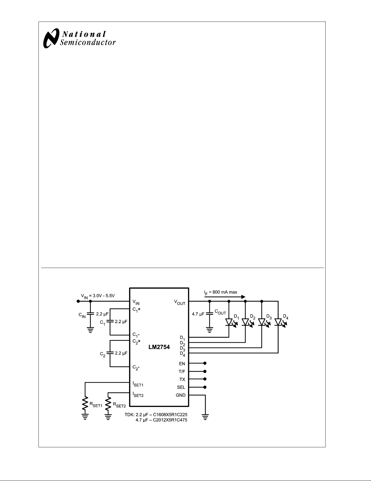
Typical Application Circuit
20202801
© 2006 National Semiconductor Corporation DS202028 www.national.com
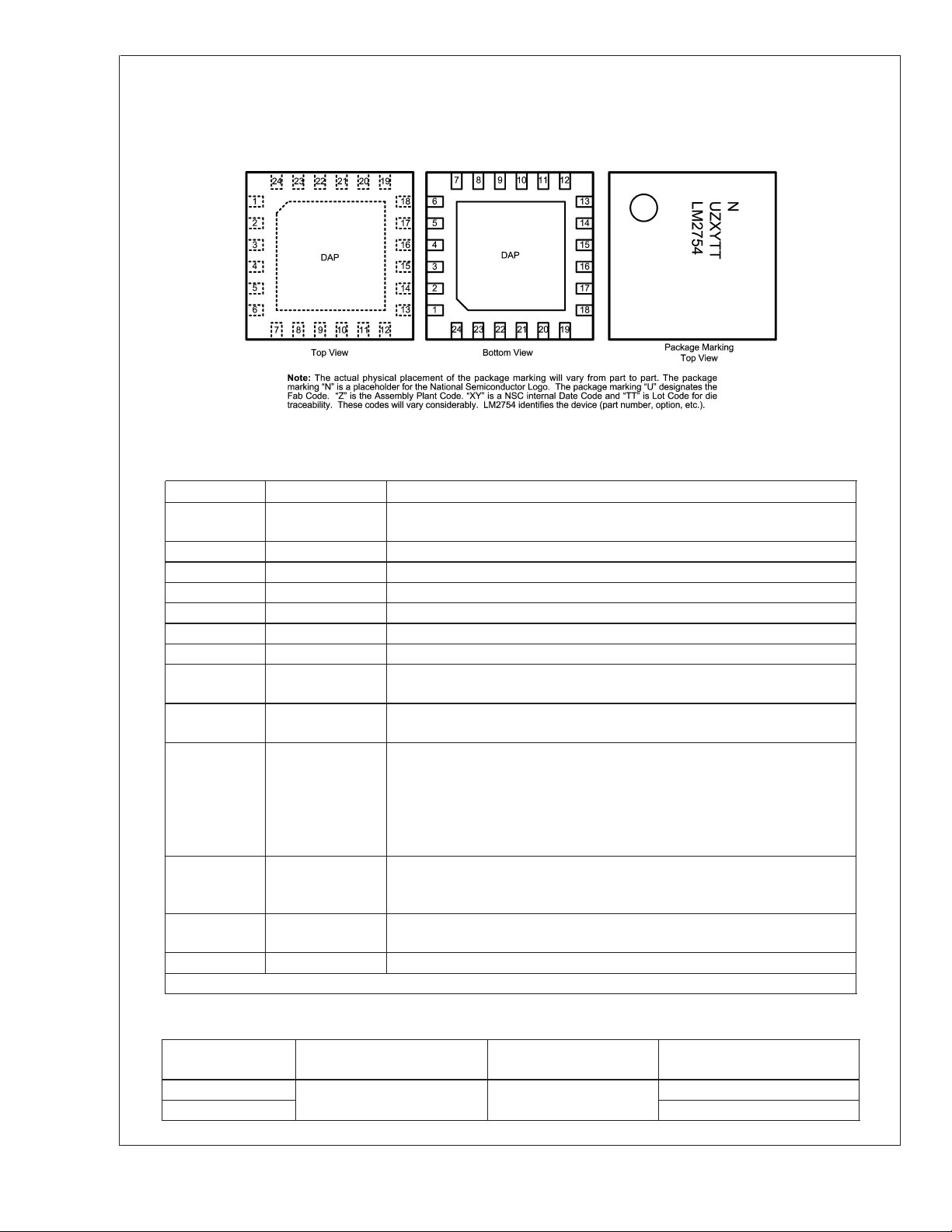
Connection Diagram
LM2754
Pin Descriptions
Pin Name Description
23,24 V
22 V
8V
12, 13, 14, 15 D1, D2, D3, D4* Regulated Current Sink Inputs. (* See SEL PIN description)
1, 2, 7, 5 C
3 GND
9, 16, 17 GND Ground Connection. Connect GND and GND
21 EN Enable Control Pin. Logic High = Normal Operation in Torch Mode.
20 T/F Torch/Flash Control Pin. Logic High = Flash Mode. Logic Low = Torch Mode.
10, 11 I
19 TX RF PA synchronization control pin. Logic High = Force Torch Mode. Logic Low
18 SEL D
4, 6 No Connect Do not connect to any node.
Note: EN, T/F, TX, and SEL pins each have a 500kΩ resistor connected internally to GND
LM2754
24-pin No-Pullback Leadless Leadframe Package (LLP-24)
4mm x 4mm x 0.8mm
NS Package Number SQA24A
INSW
Input Voltage Connection for Switch Array. Pins 23 and 24 are connected
internally on the die. Connect V
IN
OUT
+, C1-, C2+, C2- Flying Capacitor Connections.
1
SW
Input Voltage Connection. Connect VINand V
Output Voltage. Connect to LED Anodes.
Switch Array Ground Connection. Connect GND and GNDSWpins together.
Logic Low = Device Shut-Down. (See Note)
Device must be enabled for Torch or Flash to operate. (See Note)
SET1,ISET2
Current Set Resistor Connections. Connect 1% resistors to ground to set the
desired current through the LEDs. LED current is approximated by the
equation: 800 x (1.25V ÷ R). This equation corresponds to the current through
one current sink. Total LED current is equal to the sum of currents through all
current sinks connected to the LED. The equation used for Torch (I
Flash (I
) resistors are the same.
SET2
= Normal Operation. (See Applications Information section for the full
operational description) (See Note)
Control Pin. Logic Low = Normal 4-LED Operation. Logic High = Disable
4
LED Input. Connect D4to V
D
4
and V
IN
when not used. (See Note)
OUT
pins together.
INSW
INSW
SW
pins together.
pins together.
20202802
SET1
) and
Ordering Information
Order Number Package Description Package Marking Supplied as Tape and Reel
LM2754SQ No-Pullback
LM2754SQX 4500
www.national.com 2
LLP-24
UZXYTT
LM2754
(Units)
1000
LM2754
Absolute Maximum Ratings (Notes 1, 2)
If Military/Aerospace specified devices are required,
please contact the National Semiconductor Sales Office/
Distributors for availability and specifications.
V
IN,VOUT
EN, T/F, TX, SEL pins -0.3V to (V
pins -0.3V to 6.0V
+ 0.3V)
IN
Operating Ratings (Notes 1, 2)
Input Voltage (V
Junction Temperature Range (T
Ambient Temperature Range (T
(Note 5) -40˚C to +85 ˚C
) 2.8V to 5.5V
IN
) -40˚C to +125˚C
J
)
A
w/ 6.0V max
Continuous Power Dissipation
(Note 3) Internally Limited
Junction Temperature
(T
J-MAX-ABS
) 150˚C
Thermal Information
Junction-to-Ambient Thermal Resistance,
LLP-24 Package (θ
) (Note 6) 42˚C/W
JA
Storage Temperature Range -65˚C to 150˚C
Lead Temp. (Soldering, 5 sec.) 260˚C
ESD Rating (Note 4)
Human Body Model 2kV
Electrical Characteristics (Notes 2, 7)
Limits in standard typeface are for TJ= 25˚C, and limits in boldface type apply over the full operating junction temperature
range (-40˚C to +125 ˚C). Unless otherwise noted, specifications apply to the LM2754 Typical Application Circuit (pg.1) with
V
(IN, INSW)
= 3.6V, VEN= 1.8V, V
Symbol Parameter Conditions Min Typ Max Units
V
SETx
I
Dx/ISETx
I
Pin Voltage R
SETx
LED Current to Set Current
Ratio (Note 11)
V
HR
Current Sink Headroom
Voltage (Note 10)
V
OUT
R
OUT
I
Q
I
SD
f
SW
V
IH
V
IL
I
IH
Output Voltage 1x Mode, IDx= 0mA 4.7 V
Output Impedance 1x Mode 0.25 Ω
Quiescent Supply Current 1x Mode, IDx= 0mA 0.7 mA
Shutdown Supply Current VEN= 0V 0.1 1 µA
Switching Frequency 0.7 1 1.3 MHz
Logic Input High Input Pins: EN, T/F, TX, SEL 1.2 V
Logic Input Low Input Pins: EN, T/F, TX, SEL 0.4
Logic Input High Current
(Note 9)
I
IL
Logic Input Low Current
(Note 9)
Note 1: Absolute Maximum Ratings indicate limits beyond which damage to the component may occur. Operating Ratings are conditions under which operation of
the device is guaranteed. Operating Ratings do not imply guaranteed performance limits. For guaranteed performance limits and associated test conditions, see the
Electrical Characteristics tables.
Note 2: All voltages are with respect to the potential at the GND pin.
Note 3: Internal thermal shutdown circuitry protects the device from permanent damage. Thermal shutdown engages at T
120˚C (typ.).
Note 4: The Human-body model is a 100 pF capacitor discharged through a 1.5kΩ resistor into each pin.
Note 5: In applications where high power dissipation and/or poor package thermal resistance is present, the maximum ambient temperature may have to be
derated. Maximum ambient temperature (T
dissipation of the device in the application (P
following equation: T
Note 6: Junction-to-ambient thermal resistance (θ
standard JESD51-7. The test board is a 4 layer FR-4 board measuring 102mm x 76mm x 1.6mm. The 2 imbedded copper layers cover roughly the same area as
the board. Thickness of copper layers are 70µm/35µm/35µm/70µm (2oz/1oz/1oz/2oz). Thermal vias are placed between the die attach pad in the 1st copper layer
A-MAX=TJ-MAX-OP
= 0V, VTX= 0V, V
T/F
SETx
IDx= 50mA to 100mA −7% 795 +7% mA/mA
I
= 200mA −11.5% 820 +11.5%
Dx
IDx= 200mA 550 mV
I
= 50mA 150
Dx
1.5x Mode, I
2x Mode, I
1.5x Mode 1.3
2x Mode 1.5
1.5x Mode, I
2x Mode, I
V
(EN, T/F, TX, SEL)
V
(EN, T/F, TX, SEL)
) is dependent on the maximum operation junction temperature (T
A-MAX
), and the junction-to ambient thermal resistance of the part/package in the application (θJA), as given by the
D-MAX
-(θJAxP
).
D-MAX
) is taken from a thermal modeling result, performed under the conditions and guidelines set forth in the JEDEC
JA
= 0V, CIN=C1=C2= 2.2µF, C
SEL
= 4.7µF. (Note 8)
OUT
= 20kΩ −3.5% 1.244 +3.5% V
= 0mA 4.7
Dx
= 0mA 5.1
Dx
= 0mA 3.4
Dx
= 0mA 6.3 8
Dx
= 1.8V 4 µA
= 0V 0.5 µA
=150˚C (typ.) and disengages at TJ=
J
= 125oC), the maximum power
J-MAX-OP
www.national.com3
Electrical Characteristics (Notes 2, 7) (Continued)
and the 2nd copper layer. Ambient temperature in simulation is 22˚C, still air. Power dissipation is 1W.
LM2754
The value of θ
conditions. In applications where high maximum power dissipation exists (high V
For more information on these topics, please refer to Application Note 1187: Leadless Leadframe Package (LLP) and the Power Efficiency and Power
Dissipation section of this datasheet..
Note 7: Min and Max limits are guaranteed by design, test, or statistical analysis. Typical numbers are not guaranteed, but do represent the most likely norm.
Note 8: C
Note 9: There is a 500kΩ resistor connected internally between each logic pin (EN, T/F, TX, SEL) and GND.
Note 10: Headroom Voltage (V
measured from V
Note 11: I
of the LM2754 in LLP-24 could fall in a range as wide as 35oC/W to 150oC/W (if not wider), depending on PWB material, layout, and environmental
JA
IN,COUT,C1,C2
Dx/ISETx
: Low-ESR Surface-Mount Ceramic Capacitors (MLCCs) used in setting electrical characteristics
) is the voltage across the current sinks (VDx) at which the current falls to 95% of the nominal programmed current. VHRis
to GND. If the headroom voltage requirement is not met, LED current regulation will be compromised.
Dx
Ratio was tested with the Charge Pump in a gain of 1x.
HR
, high Gain, high I
IN
), special care must be paid to thermal dissipation issues.
OUT
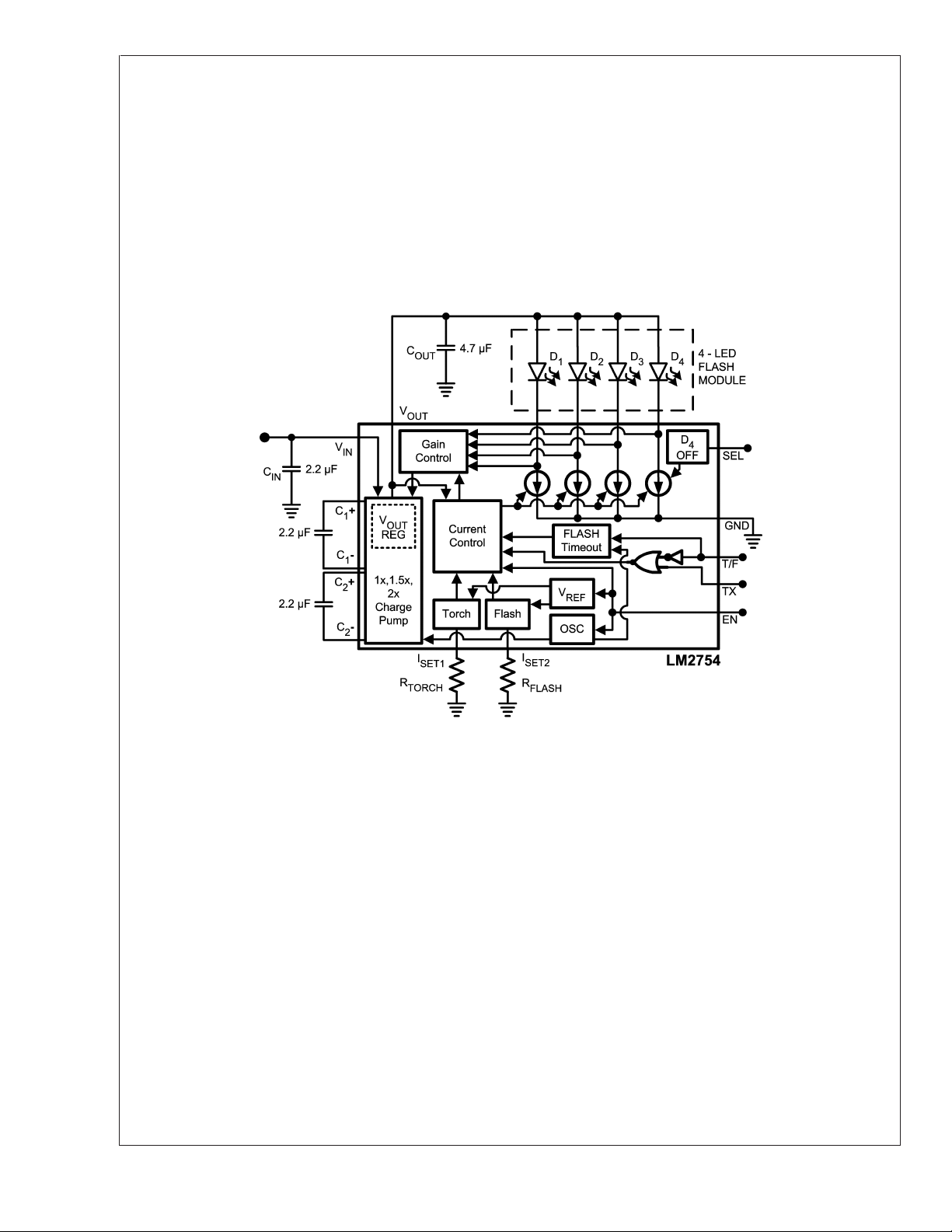
Block Diagram
www.national.com 4
20202803

LM2754
Typical Performance Characteristics Unless otherwise specified: T
3.6V, V
EN=VIN,VT/F=VTX=VSEL
capacitors (MLCC’s).
Quiescent Current vs. Input Voltage Shutdown Current vs. Input Voltage
Dx Current vs. R
= 0V, CIN=C1=C2= 2.2µF, C
SET
20202804
= 4.7µF. Capacitors are low-ESR multi-layer ceramic
OUT
Dx Current vs. Headroom Voltage
= 25˚C, VDx= 1V, V
A
(IN, INSW)
20202805
=
20202806 20202807
Efficiency vs. Input Voltage Oscillator Frequency vs. Input Voltage
20202808 20202809
www.national.com5

Typical Performance Characteristics Unless otherwise specified: T
3.6V, V
LM2754
EN=VIN,VT/F=VTX=VSEL
capacitors (MLCC’s). (Continued)
Flash Mode with TX Pulse Torch to Flash Mode
= 0V, CIN=C1=C2= 2.2µF, C
= 4.7µF. Capacitors are low-ESR multi-layer ceramic
OUT
= 25˚C, VDx= 1V, V
A
(IN, INSW)
=
VIN= 3.6V, Load = 700mA (Flash), LED = PWF1
CH1 (TOP): V
CH2 (BOTTOM): I
Time scale: 1ms/Div
; Scale: 1V/Div, DC Coupled
TX
; Scale: 200mA/Div
LED
20202810
Torch to Flash Mode
Rising Edge
VIN= 3.6V, Load = 200mA/800mA (Torch/Flash), LED = PWF1
CH1 (TOP): V
CH2 (MIDDLE): V
CH3 (BOTTOM): I
Time scale: 400µs/Div
; Scale: 1V/Div, DC Coupled
IN
; Scale: 1V/Div, DC Coupled
OUT
; Scale: 200mA/Div
IN
20202812
VIN= 3.6V, Load = 200mA/800mA (Torch/Flash), LED = PWF1
CH1 (TOP): V
CH2 (MIDDLE): V
CH3 (BOTTOM): I
Time scale: 100ms/Div
; Scale: 1V/Div, DC Coupled
IN
; Scale: 1V/Div, DC Coupled
OUT
; Scale: 200mA/Div
IN
20202811
Flash to Torch Mode
Falling Edge
VIN= 3.6V, Load = 800mA/200mA (Flash/Torch), LED = PWF1
CH1 (TOP): V
CH2 (MIDDLE): V
CH3 (BOTTOM): I
Time scale: 100µs/Div
; Scale: 1V/Div, DC Coupled
IN
; Scale: 1V/Div, DC Coupled
OUT
; Scale: 200mA/Div
IN
20202813
www.national.com 6

LM2754
Typical Performance Characteristics Unless otherwise specified: T
3.6V, V
EN=VIN,VT/F=VTX=VSEL
capacitors (MLCC’s). (Continued)
Battery Ripple, Gain = 1.5x Battery Ripple, Gain = 2x
VIN= Li-Ion Battery at 3.7V, Load = 400mA, LED = PWF1
CH1 (MID-TOP): V
CH2 (MID-BOTTOM): V
CH3 (TOP): V
CH4 (BOTTOM): I
Time scale: 1µs/Div
; Scale: 20mV/Div, AC Coupled
OUT
; Scale: 50mV/Div, AC Coupled
IN
; Scale: 1V/Div, DC Coupled
IN
; Scale: 500mA/Div
IN
Startup and Shutdown Response
Torch Mode (400mA)
= 0V, CIN=C1=C2= 2.2µF, C
20202814
= 4.7µF. Capacitors are low-ESR multi-layer ceramic
OUT
VIN= Li-Ion Battery at 3.7V, Load = 400mA, LED = PWF1
CH1 (MID-TOP): V
CH2 (MID-BOTTOM): V
CH3 (TOP): V
CH4 (BOTTOM): I
Time scale: 1µs/Div
; Scale: 1V/Div, DC Coupled
IN
IN
= 25˚C, VDx= 1V, V
A
; Scale: 20mV/Div, AC Coupled
OUT
; Scale: 50mV/Div, AC Coupled
IN
; Scale: 500mA/Div
20202815
(IN, INSW)
=
VIN= 3.6V, Load = 400mA, LED = PWF1
CH1 (TOP): V
CH4 (MIDDLE): I
CH3 (BOTTOM): I
Time scale: 100ms/Div
; Scale: 1V/Div, DC Coupled
OUT
; Scale: 200mA/Div
IN
; Scale: 200mA/Div
OUT
20202816
www.national.com7

Application Information
LM2754
CIRCUIT DESCRIPTION
The LM2754 is an adaptive 1x/1.5x/2x CMOS charge pump,
optimized for driving Flash LEDs in camera phone and other
portable applications. It provides four constant current inputs, each capable of sinking up to 200mA for Flash mode,
and 100mA for Torch mode.
Each LED is driven from V
four current sinks. LED drive current for Torch mode is
programmed by connecting a resistor, R
set pin, I
. LED drive current for Flash mode is set by
SET1
connecting a resistor, R
Torch mode is enabled by the EN pin, and the transition from
Torch to Flash mode is controlled by the T/F pin. This device
also has an option to disable the D
pin, for Flash LED modules with only 3 LEDs.
To prevent high battery load during a simultaneous RF PA
transmission pulse and Flash condition, this device has a
Flash interrupt pin (TX) to reduce the LED current to the
Torch mode level for the duration of the RF PA transmission
pulse.
CHARGE PUMP
The input to the 1x/1.5x/2x charge pump is connected to the
pin, and the loosely regulated output of the charge pump
V
IN
is connected to the V
OUT
charge pump has both open loop and closed loop modes of
operation. Under no-load conditions, open loop operation
occurs when V
is equal to the product of the input voltage
OUT
and the charge pump gain, and is less than the nominal
output regulation voltage. Over the recommended input voltage range of 3.0V to 5.5V, unloaded open loop operation will
only occur in 1x and 1.5x gains. When the LM2754 is in
closed loop operation with no-load, the voltage at V
loosely regulated to 4.7V (typ.) for the 1x and 1.5x gains, and
5.1V (typ.) for the 2x gain. When under load, the voltage at
can be less than the target regulation voltage while the
V
OUT
charge pump is still in closed loop operation. This is due to
the load regulation topology of the LM2754.
The charge pump gain transitions are actively selected to
maintain regulation based on LED forward voltage and load
requirements. The charge pump only transitions to higher
gains, from 1x to 1.5x and 1.5x to 2x. Each transition from
one gain to the next takes 125ms (typ.) for Torch mode and
2ms (typ.) for Flash mode. Once the charge pump transitions
to a higher gain, it will remain at that gain for as long as the
device remains enabled. Shutting down and then re-enabling
the device resets the gain mode to the minimum gain required to maintain the load.
SOFT START
The LM2754 contains internal soft-start circuitry to limit inrush currents when the part is enabled. Soft start is implemented internally with a controlled turn-on of the internal
voltage reference.
CURRENT LIMIT PROTECTION
The LM2754 charge pump contains current limit protection
circuitry that protects the device during V
where excessive current is drawn. Output current is limited
to 1.2A (typ.).
and connected to one of the
OUT
, to the current
SET1
, to the current set pin, I
SET2
current sink via the SEL
4
pin. The device’s loosely-regulated
fault conditions
OUT
OUT
SET2
LOGIC CONTROL PINS
There are 4 logic control pins for the LM2754. All pins are
active-High logic (High = Function ON). There is an internal
pull-down resistor (500kΩ typ.) connected between each
logic pin and GND. The operating modes for the part function
according to the Table below:
EN T/F TX SEL Mode
0 X X X Part in Shutdown
10X0
.
10X1
1100
1101
Part Enabled, Current set by
R
SET1,D1-4
Active
Part Enabled, Current set by
R
SET1,D1-3
Active, D4Disabled
Part Enabled, Current set by
R
SET2,D1-4
Active
Part Enabled, Current set by
R
SET2,D1-3
Active, D4Disabled
Part Enabled, Current set by
1110
R
, TX signal from RF PA,
SET1
Active
D
1-4
Part Enabled, Current set by
1111
, TX signal from RF PA,
R
SET1
Active, D4Disabled
D
1-3
EN PIN (TORCH)
The EN pin is the master enable pin for the part. When the
voltage on this pin is Low (
mode. In this mode, all internal circuitry is OFF, V
disconnected from the V
<
supply current (
is High (
is
regulate the output voltage to its nominal value. When the
>
1µA typ.). When the voltage on the EN pin
1.2V), the part will activate the charge pump and
<
0.4V), the part is in shutdown
, and the part consumes very little
IN
OUT
is
output voltage reaches its regulation level, the current sinks
will turn on and sink the current programmed by R
SET1
(assuming the logic on T/F is Low). Enabling the device is
also referred to as Torch Mode. For correct start-up sequencing, power must be applied to V
before a High logic
IN
signal is applied to the EN pin.
T/F PIN (FLASH) AND FLASH TIMEOUT
A logic Low (
<
0.4V) signal on the T/F pin disables the Flash
mode, defaulting the current through the LEDs to the Torch
level programmed by R
. Applying a logic High (>1.2V)
SET1
signal to T/F places the device in Flash mode, with the LED
current set by R
SET2
.
Flash Timeout Protection Circuitry disables the current sinks
when the signal on T/F is held high for more than 1 second
(typ). This prevents the device from self-heating due to the
high power dissipation during Flash conditions. During the
timeout condition, voltage will still be present on V
OUT
but
the current sinks will be shut off, resulting in no current
through the Flash LEDs. When the device goes into a timeout condition, placing a logic Low signal on EN will reset the
timeout and a subsequent logic High signal on EN will return
the device to normal operation. Flash timeout is not active
during TX mode.
TX PIN
The TX pin on the LM2754 disables the Flash operation
during a RF PAtransmission pulse, and sets the LED current
to the Torch level programmed by R
for the duration of
SET1
that pulse. At the end of each transmission interrupt pulse
www.national.com 8

Application Information (Continued)
signal on the TX pin, the LED current level returns to the
Flash current level set by R
>
typical logic High (
1.2V) and logic Low (<0.4V) signal
levels. Flash Timeout is not active during the TX mode
operation.
SEL PIN
Connecting the SEL pin to a logic Low (
the device in normal operation, with all 4 current sinks active.
To accommodate Flash LED modules with only 3 LEDs,
>
place a logic High (
the current sink D
1.2V) signal on the SEL pin to disable
. If only 3 current sinks are used, the
4
200mA per current sink recommendation still applies, and
the maximum Flash current will be 600mA. Connect D
when the logic in the SEL pin is High. Optional use of
V
OUT
the SEL pin is to reduce the LED current used for Torch or
Flash by 25% for high battery load conditions.
SETTING LED CURRENTS
The current through the LEDs connected to D
simply by connecting an appropriately sized resistor (R
between the I
mode and the I
pin of the LM2754 and GND for Torch
SET1
pin and GND for Flash Mode. The LED
SET2
currents are proportional to the current that flows out of the
pin and are a factor of approximately 800 times greater
I
SETx
than the I
current. The feedback loop of an internal
SETx
amplifier sets the voltage of the I
statements above are simplified in the equations below:
= 800 x(V
I
Dx
R
= 800 x (1.25V / IDx)
SET
The maximum recommended current through each current
sink is 100mA during Torch mode and 200mA during Flash
mode. Maximum recommended total Flash current with all 4
current sinks used is 800mA (max 200mA per current sink).
Using the part in conditions where the junction temperature
might rise above the rated maximum requires that the operating ranges and/or conditions be de-rated. The printed circuit board also must be carefully laid out to account for high
thermal dissipation in the part.
PARALLEL DX OUTPUTS FOR INCREASED CURRENT DRIVE
Outputs D
may be connected together to drive a one or
1-4
two LEDs at higher currents. In applications using a single
LED, all four parallel current sinks of equal value drive the
single LED. For this type of configuration, the LED current
should be programmed so that the current through each of
the outputs is 25% of the total desired LED current. For
example, if 200mA is the desired drive current for the single
LED, R
should be selected such that the current through
SET
each of the current sink inputs is 50mA. Similarly, if two
LEDs are to be driven by pairing up the D
), R
D
3-4
should be selected such that the current through
SET
each current sink input is 50% of the desired LED current.
Connecting the outputs in parallel does not affect internal
operation of the LM2754 and has no impact on the Electrical
Characteristics and limits previously presented. The available diode output current, maximum diode voltage, and all
other specifications provided in the Electrical Characteristics
table apply to this parallel output configuration, just as they
do to the standard 4-LED application circuit.
. The TX pin responds to the
SET2
<
0.4V) signal places
1-4
pin to 1.25V (typ.). The
SET
SET/RSET
)
inputs (i.e D
1-4
4
can be set
SETx
1-2
LM2754
Maximum recommended LED current for any configuration
is 200mA per current sink, and 800mA total. For situations
where only 3 current sinks will be used for the application,
see the SEL PIN operation section.
CAPACITOR SELECTION
The LM2754 requires 4 external capacitors for proper operation. Surface-mount multi-layer ceramic capacitors are recommended. These capacitors are small, inexpensive and
have very low equivalent series resistance (ESR
typ.). Tantalum capacitors, OS-CON capacitors, and aluminum electrolytic capacitors are not recommended for use
with the LM2754 due to their high ESR, as compared to
ceramic capacitors.
to
For most applications, ceramic capacitors with X7R or X5R
temperature characteristic are preferred for use with the
LM2754. These capacitors have tight capacitance tolerance
±
(as good as
±
(X7R:
10%) and hold their value over temperature
15% over -55˚C to 125˚C; X5R:±15% over -55˚C to
85˚C).
Capacitors with Y5V or Z5U temperature characteristic are
)
generally not recommended for use with the LM2754. Capacitors with these temperature characteristics typically
have wide capacitance tolerance (+80%, -20%) and vary
significantly over temperature (Y5V: +22%, -82% over -30˚C
to +85˚C range; Z5U: +22%, -56% over +10˚C to +85˚C
range). Under some conditions, a nominal 1µF Y5V or Z5U
capacitor could have a capacitance of only 0.1µF. Such
detrimental deviation is likely to cause Y5V and Z5U capacitors to fail to meet the minimum capacitance requirements of
the LM2754.
The voltage rating of the output capacitor should be 10V or
more. For example, a 10V 0603 4.7µF output capacitor (TDK
C1608X5R1A475) is acceptable for use with the LM2754, as
long as the capacitance on the output does not fall below a
minimum of 3µF in the intended application. All other capacitors should have a voltage rating at or above the maximum
input voltage of the application and should have a minimum
capacitance of 1µF.
POWER EFFICIENCY
Efficiency of LED drivers is commonly taken to be the ratio of
power consumed by the LEDs (P
the input of the part (P
). With a 1x/1.5x/2x charge pump,
IN
) to the power drawn at
LED
the input current is equal to the charge pump gain times the
output current (total LED current). The efficiency of the
LM2754 can be predicted as follows:
=NxV
P
LED
PIN=VINxI
PIN=VINx (GainxNxI
E=(P
LEDxILED
LED÷PIN
IN
LED+IQ
)
For a simple approximation, the current consumed by inter-
,
nal circuitry (I
) can be neglected, and the resulting effi-
Q
ciency will become:
÷(VINx Gain)
LED
Neglecting I
E=V
will result in a slightly higher efficiency predic-
Q
tion, but this impact will be negligible due to the value of I
being very low compared to the typical Torch and Flash
current levels (100-800mA). It is also worth noting that efficiency as defined here is in part dependent on LED voltage.
Variation in LED voltage does not affect power consumed by
the circuit and typically does not relate to the brightness of
the LED. For an advanced analysis, it is recommended that
power consumed by the circuit (V
) be evaluated rather
INxIIN
than power efficiency.
<
20mΩ
)
Q
www.national.com9

Application Information (Continued)
THERMAL PROTECTION
LM2754
Internal thermal protection circuitry disables the LM2754
when the junction temperature exceeds 150˚C (typ.). This
feature protects the device from being damaged by high die
temperatures that might otherwise result from excessive
power dissipation. The device will recover and operate normally when the junction temperature falls below 120˚C (typ.).
It is important that the board layout provide good thermal
conduction to keep the junction temperature within the specified operating ratings.
POWER DISSIPATION
The power dissipation (P
) can be approximated with the equations below. P
ture (T
J
DISSIPATION
is the power generated by the 1x/1.5x/2x charge pump, P
is the power consumed by the LEDs, TAis the ambient
temperature, and θ
is the junction-to-ambient thermal re-
JA
sistance for the LLP-24 package. V
the LM2754, V
is the programmed LED current.
I
LED
is the nominal LED forward voltage, and
LED
P
DISSIPATION=PIN-PLED
= [Gain x VINx(4xI
) and junction tempera-
is the input voltage to
IN
)]−(V
LED
LED
x4xI
LED
T
J=TA
+(P
DISSIPATION
x θJA)
The junction temperature rating takes precedence over the
ambient temperature rating. The LM2754 may be operated
outside the ambient temperature rating, so long as the junction temperature of the device does not exceed the maximum operating rating of 125˚C. The maximum ambient temperature rating must be derated in applications where high
power dissipation and/or poor thermal resistance causes the
junction temperature to exceed 125˚C.
PCB Layout Considerations
The LLP is a leadframe based Chip Scale Package (CSP)
with very good thermal properties. This package has an
exposed DAP (die attach pad) at the center of the package
IN
LED
)
measuring 2.6mm x 2.6mm. The main advantage of this
exposed DAP is to offer lower thermal resistance when it is
soldered to the thermal land on the PCB. For PCB layout,
National highly recommends a 1:1 ratio between the package and the PCB thermal land. To further enhance thermal
conductivity, the PCB thermal land may include vias to a
ground plane. For more detailed instructions on mounting
LLP packages, please refer to National Semiconductor Application Note AN-1187.
www.national.com 10

Physical Dimensions inches (millimeters) unless otherwise noted
LM2754 800mA Switched Capacitor Flash LED Driver with Time-Out Protection
24-Pin LLP
NS Package Number SQA24A
National does not assume any responsibility for use of any circuitry described, no circuit patent licenses are implied and National reserves
the right at any time without notice to change said circuitry and specifications.
For the most current product information visit us at www.national.com.
LIFE SUPPORT POLICY
NATIONAL’S PRODUCTS ARE NOT AUTHORIZED FOR USE AS CRITICAL COMPONENTS IN LIFE SUPPORT DEVICES OR SYSTEMS
WITHOUT THE EXPRESS WRITTEN APPROVAL OF THE PRESIDENT AND GENERAL COUNSEL OF NATIONAL SEMICONDUCTOR
CORPORATION. As used herein:
1. Life support devices or systems are devices or systems
which, (a) are intended for surgical implant into the body, or
(b) support or sustain life, and whose failure to perform when
properly used in accordance with instructions for use
2. A critical component is any component of a life support
device or system whose failure to perform can be reasonably
expected to cause the failure of the life support device or
system, or to affect its safety or effectiveness.
provided in the labeling, can be reasonably expected to result
in a significant injury to the user.
BANNED SUBSTANCE COMPLIANCE
National Semiconductor follows the provisions of the Product Stewardship Guide for Customers (CSP-9-111C2) and Banned Substances
and Materials of Interest Specification (CSP-9-111S2) for regulatory environmental compliance. Details may be found at:
www.national.com/quality/green.
Lead free products are RoHS compliant.
National Semiconductor
Americas Customer
Support Center
Email: new.feedback@nsc.com
Tel: 1-800-272-9959
www.national.com
National Semiconductor
Europe Customer Support Center
Fax: +49 (0) 180-530 85 86
Email: europe.support@nsc.com
Deutsch Tel: +49 (0) 69 9508 6208
English Tel: +44 (0) 870 24 0 2171
Français Tel: +33 (0) 1 41 91 8790
National Semiconductor
Asia Pacific Customer
Support Center
Email: ap.support@nsc.com
National Semiconductor
Japan Customer Support Center
Fax: 81-3-5639-7507
Email: jpn.feedback@nsc.com
Tel: 81-3-5639-7560
 Loading...