

November 2006
LM2753
High Power Switched Capacitor Voltage Convertor/Flash
LED Driver
LM2753 High Power Switched Capacitor Voltage Convertor/Flash LED Driver
General Description
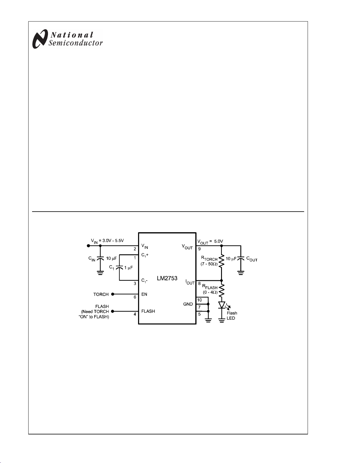
The LM2753 is capable of driving a Flash LED with a pulsed
current of 400mA at an input voltage of 3.6V. A switched capacitor doubler, the LM2753 provides a regulated 5V output
(V
) over an input supply range of 3.0V to 5.5V. The
OUT
switched output, I
provide maximum current to a Flash LED. Flash LED current
is set via a ballast resistor. Continuous illumination current
(Torch Mode) is programmed by connecting a resistor between I
cost ceramic capacitors.
LM2753 uses Pulse Frequency Modulation (PFM) regulation.
Typical operating frequency is 725kHz. Under no-load conditions, LM2753 operates on only 60µA. If the output is connected to ground, the charge pump stays in the gain of 1
which helps limit the input current to 300mA (typ.)
LM2753 is available in a 10-pin No Pullback Leadless Leadframe Package: LLP-10.
OUT
and V
, takes less than 10ns to turn on and
OUT
. This device uses only three small, low-
OUT
Typical Application Circuit
Features
Input Voltage Range: 3.0V to 5.5V
■
Regulated 5V Output
■
250mA Output Current with a 3.6V input
■
400mA Pulsed Output Current (up to 500ms duration)
■
60µA (typ.) Quiescent Current
■
PFM Regulation
■
Inductor-less solution: requires only 3 small capacitors
■
<1µA Typical Shutdown Current
■
10-pin LLP Package (No Pullback):
■
3mm x 3mm x 0.8mm
Applications
Cell Phone Camera Flash
■
General Purpose Regulated Voltage Output, High Current
■
Supply
20140601
© 2006 National Semiconductor Corporation 201406 www.national.com
Connection Diagram
LM2753
Pin Descriptions
Pin # Name Description
1 C
2 V
3 C
4 FLASH Flash Logic Input Pin. Logic HIGH = Flash Output On, Logic LOW = Flash Output Off. There
5 GND Connect to Ground.
6 EN Enable Pin. Logic HIGH = Enable, Logic LOW = Shut Down. There is an internal pulldown
7 GND Connect to Ground.
8 I
9 V
10 GND Connect to Ground
OUT
OUT
10-Pin LLP Package (LLP10) No Pullback
NS Package Number SDA10A
1+
IN
1-
Flying capacitor connection.
Input Voltage Connection. Input Voltage Range: 3.0V to 5.5V.
Flying Capacitor connection.
is an internal pulldown of 300kΩ between FLASH and GND.
of 300kΩ between EN and GND
Flash Output. On/Off Control via FLASH Pin.
5V Regulated Output.
LM2753
3mm X 3mm x 0.8mm
20140605
Ordering Information
Output Voltage Ordering Number Package Mark ID Package Supplied As
5.0V LM2753SD D004B SDA10A
5.0V LM2753SDX D004B 4500 Units, Tape and
www.national.com 2
Non-Pullback
LLP
1000 Units, Tape and
Reel
Reel
LM2753
Absolute Maximum Ratings (Notes 1, 2)
If Military/Aerospace specified devices are required,
please contact the National Semiconductor Sales Office/
Distributors for availability and specifications.
If Military/Aerospace specified devices are required, please
contact the National semiconductor Sales/Office/Distributors
for availability and specifications.
VIN Pin: Voltage to Ground
EN, Flash pins: Voltage to GND −0.3V to (VIN+0.3)
Continuous Power Dissipation (Note
3) Internally Limited
Junction Temperature (T
J-MAX-ABS
)
−0.3V to 6.0V
w/ 6.0V max
150°C
Operating Ratings (Notes 1, 2)
Input Voltage Range 3.0V to 5.5V
EN, Flash Input Voltage Range 0V to V
Junction Temperature (TJ) Range
Ambient Temperature (TA) Range
-40°C to 120°C
-40°C to 85°C
(Note 5)
Thermal Properties
Junction-to-Ambient Thermal
Resistance, LLP-10 55°C/W
Package (θJA) (Note 6)
Storage Temperature Range −65°C to 150°C
Maximum Lead Temperature 265°C
(Soldering, 10sec.)
ESD Rating (Note 4)
Human-body model:
Machine model:
2kV
200V
Electrical Characteristics (Notes 2, 7)
Limits in standard typeface are for TA = 25ºC. Limits in boldface type apply over the full operating ambient temperature range (-40°
C ≤ TA ≤ +85°C) . Unless otherwise noted, specifications apply to the LM2753 Typical Application Circuit (pg. 1) with: VIN = 3.6V,
V(EN) = V
Symbol Parameter Conditions Min Typ Max Units
V
OUT
I
VOUT
I
OUT
I
Q
I
SD
R
OUT
f
sw
V
IH
V
IL
I
IH
I
IL
t
ON
t
FLASH
Note 1: Absolute Maximum Ratings indicate limits beyond which damage to the component may occur. Operating Ratings are conditions under which operation
of the device is guaranteed. Operating Ratings do not imply guaranteed performance limits. For guaranteed performance limits and associated test conditions,
see the Electrical Characteristics tables.
Note 2: All voltages are with respect to the potential at the GND pin.
Note 3: Internal thermal shutdown circuitry protects the device from permanent damage. Thermal shutdown engages at TJ=125°C (typ.).
Note 4: The Human body model is a 100 pF capacitor discharged through a 1.5 kΩ resistor into each pin. The machine model is a 200pF capacitor discharged
directly into each pin. MIL-STD-883 3015.7
V(FLASH) = GND, C1 = 1.0µF, CIN = C
IN,
Output Voltage
Continuous Load Current
Pulsed Flash Current V(FLASH) = 1.8V
Quiescent Current I
= 10.0µF (Note 8).
OUT
3.0V ≤ VIN ≤ 5.5V,
I
≤ 100mA
OUT
3.0V ≤ VIN ≤ 5.5V
V
= 5V (typ.)
OUT
T
= 500ms
PULSE
V
OUT
IOUT-MAX
= 0mA
= 4.1V (typ.)
4.75
(-5%)
5.0 5.25
(+5%)
200 mA
400 mA
60 80 µA
3.0V ≤ VIN ≤ 5.5V
Shutdown Supply Current V(EN) = 0V
0.1 1 µA
3.0V ≤ VIN ≤ 5.5V
V(EN) = 0V
0.2
3.0V ≤ VIN ≤ 5.5V
TA = 85°C
Output Impedance VIN = 3.2V 5.3
Switching Frequency
3.0V ≤ VIN ≤ 5.5V
475 725 950
Logic Input High Input Pins: EN, FLASH 1.20 V
Logic Input Low Input Pins: EN, FLASH 0 .30 V
Logic Input High Current V(EN) = V(FLASH) = 3.0V 10 µA
Logic Input Low Current V(EN) = V(FLASH) = 0V 10 nA
Turn-On Time (Note 9) 640 µs
Flash Turn-On Time (Note 10) V(FLASH) = 3.6V 10 ns
IN
IN
V
Ω
kHz
V
3 www.national.com
Note 5: In applications where high power dissipation and/or poor package thermal resistance is present, the maximum ambient temperature may have to be
derated. Maximum ambient temperature (T
dissipation of the device in the application (P
LM2753
following equation: T
A-MAX
= T
J-MAX-OP
- (θJA × P
) is dependent on the maximum operating junction temperature (T
A-MAX
), and the junction-to ambient thermal resistance of the part/package in the application (θJA), as given by the
D-MAX
).
D-MAX
= 120ºC), the maximum power
J-MAX-OP
Note 6: Junction-to-ambient thermal resistance (θJA) is taken from a thermal modeling result, performed under the conditions and guidelines set forth in the
JEDEC standard JESD51-7. The test board is a 4 layer FR-4 board measuring 102mm x 76mm x 1.6mm with a 2 x 1 array of thermal vias. The ground plane on
the board is 50mm x 50mm. Thickness of copper layers are 36µm/18µm /18µm/36µm (1.5oz/1oz/1oz/1.5oz). Ambient temperature in simulation is 22°C, still air.
Power dissipation is 1W.
The value of θ
conditions. In applications where high maximum power dissipation exists (high VIN, high I
information on these topics, please refer to Application Note 1187: Leadless Leadframe Package (LLP) and the Power Efficiency and Power Dissipation
of the LM2753 in LLP-10 could fall in a range as wide as 50ºC/W to 150ºC/W (if not wider), depending on PWB material, layout, and environmental
JA
), special care must be paid to thermal dissipation issues. For more
OUT
section of this datasheet.
Note 7: Min and Max limits are guaranteed by design, test, or statistical analysis. Typical numbers are not guaranteed, but represent the most likely norm.
Note 8: CIN, C
Note 9: Turn-on time is measured from when the EN signal is pulled high until the output voltage on V
Note 10: Flash Turn-on time is measured from when the FLASH signal is pulled high until the voltage on I
, and C1: Low-ESR Surface-Mount Ceramic Capacitors (MLCCs) used in setting electrical characteristics.
OUT
crosses 90% of its final value.
OUT
crosses 90% of its final programmed value.
OUT
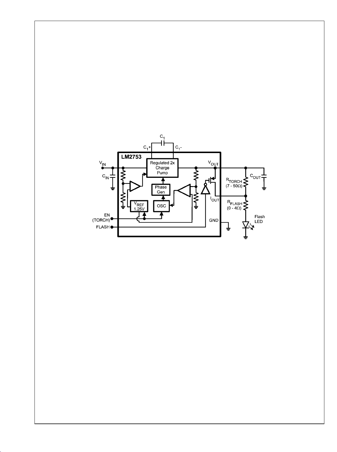
Block Diagram
20140606
www.national.com 4

LM2753
Typical Performance Characteristics Unless otherwise specified: T
GND, V(EN) = VIN, CIN = C
Quiescent Current vs. Input Voltage
Oscillator Frequency vs. Input Voltage
= 10.0µF, C1 = 1µF.
OUT
Efficiency vs. Input Voltage
20140611
Load Step Response
= 25°C, VIN = 3.6V, V(FLASH) =
A
20140610
Start-up Behavior
VIN = 3.6V, Load = 100mA
Top: VEN; Scale: 2V/Div
Bottom: V
Time scale: 100µs/Div
; Scale: 1V/Div
OUT
20140615
20140612
VIN = 3.6V, Load = 10mA - 200mA Step
Top: I
Bottom: V
Time scale: 40µs/Div
; Scale: 100mA/Div
VOUT
; Scale: 50mV/Div, AC Coupled
OUT
Flash Enable Behavior
VIN = 3.6V, No Load
Top: V
Bottom: V
Time scale: 400ns/Div
; Scale: 2V/Div
FLASH
IOUT
; Scale: 1V/Div
20140617
20140616
5 www.national.com

LM2753
Flash Pulse Response
Output Voltage Ripple
VIN = 3.6V, Load = 10mA - 400mA Step
Top: V
Middle: V
Bottom: I
; Scale: 1V/Div
FLASH
; Scale: 1V/Div
IOUT
; Scale: 100mA/Div
IOUT
Time scale: 100ms/Div
Output Voltage Ripple vs. Input Voltage
20140620
20140614
VIN = 3.6V, Load = 200mA
Plot: V
; Scale: 50mV/Div, AC Coupled
OUT
Time scale: 2µs/Div
Input Voltage Ripple
VIN = 3.6V, Load = 200mA
Plot: VIN; Scale: 50mV/Div, AC Coupled
Time scale: 4µs/Div
20140619
20140618
www.national.com 6

Application Information
CIRCUIT DESCRIPTION
The LM2753 is a Switched Capacitor Doubler with a regulated
5V output. It is capable of continuously supplying up to 200mA
at 5V to a load connected to V
Frequency Modulation and a Multi-Level Switch Array to regulate and maintain the output voltage. For higher load currents, such as during Flash operation, the output voltage is
allowed to droop to supply the necessary current. Although
there is no current limit on this device, the device will automatically default to a gain of 1 when the output is brought
below the input voltage. This configuration limits the input
current to about 300mA (typ.). The operating range for the
LM2753 is over the extended Li-Ion battery range from 2.7V
to 5.5V.
Aside from powering Flash LEDs, the LM2753 is suitable for
driving other devices with power requirements up to 200mA.
White LEDs can also be connected to this device to backlight
a cellular phone keypad and display. The LED brightness can
be controlled by applying a PWM (Pulse Width Modulation)
signal to the Enable pin (EN) during "Torch" mode, or to the
Flash pin during "Flash" mode. (see PWM BRIGHTNESS
CONTROL PROCEDURES section).
SOFT START
Soft Start is engaged when the device is taken out of Shutdown mode (EN = logic HIGH) or when voltage is supplied
simultaneously to the VIN and EN pins. During Soft Start, the
voltage on V
reference voltage is being ramped up. The output voltage is
will ramp up in proportion to the rate that the
OUT
programmed to rise from 0V to 5V in 640µs (typ.).
ENABLE MODE
The Enable logic pin (EN) disables the part and reduces the
quiescent current to 0.1µA (typ.). The LM2753 has an activehigh enable pin (LOW = shut down, HIGH = operating). The
LM2753 EN pin can be driven with a low-voltage CMOS logic
signal (1.5V logic, 1.8V logic, etc). There is an internal
300kΩ pull-down resistor between the EN and GND pins of
the LM2753.
FLASH MODE
The Flash logic pin (Flash) controls the internal FET connected between the V
LM2753 has an active-HIGH Flash pin (LOW = shut down,
OUT
and I
HIGH = operating). A logic HIGH signal must be present on
the EN pin before a logic HIGH signal is place on the Flash
input pin. The EN and Flash input pins can be connected together and controlled with the same logic signal. The turn-on
time for I
time of the device. The turn-on time for the internal FET is
in this configuration will be limited by the turn-on
OUT
typically 10ns when the device is already on (EN signal HIGH,
V
at 5V). The LM2753 Flash pin can be driven with a low-
OUT
voltage CMOS logic signal (1.5V logic, 1.8V logic, etc). There
is an internal 300kΩ pull-down resistor between the Flash and
GND pins of the LM2753.
CAPACITOR SELECTION
The LM2753 requires 3 external capacitors for proper operation. Surface-mount multi-layer ceramic capacitors are recommended. These capacitors are small, inexpensive and
have very low equivalent series resistance (ESR, ≤15mΩ
typ.). Tantalum capacitors, OS-CON capacitors, and aluminum electrolytic capacitors are generally not recommended
for use with the LM2753 due to their high ESR, as compared
to ceramic capacitors.
. This device uses Pulse
OUT
pins on the LM2753. The
OUT
For most applications, ceramic capacitors with X7R or X5R
temperature characteristic are preferred for use with the
LM2753. These capacitors have tight capacitance tolerance
(as good as ±10%), hold their value over temperature (X7R:
±15% over −55°C to 125°C; X5R: ±15% over −55°C to 85°C),
and typically have little voltage coefficient when compared to
other types of capacitors. However selecting a capacitor with
a voltage rating much higher than the voltage it will be subjected to, will ensure that the capacitance will stay closer to
the capacitor's nominal value. Capacitors with Y5V or Z5U
temperature characteristic are generally not recommended
for use with the LM2753. Capacitors with these temperature
characteristics typically have wide capacitance tolerance
(+80%, −20%), vary significantly over temperature (Y5V:
+22%, −82% over −30°C to +85°C range; Z5U: +22%, −56%
over +10°C to +85°C range), and have poor voltage coefficients. Under some conditions, a nominal 1µF Y5V or Z5U
capacitor could have a capacitance of only 0.1µF. Such detrimental deviation is likely to cause Y5V and Z5U capacitors to
fail to meet the minimum capacitance requirements of the
LM2753. Table 1 lists suggested capacitor suppliers for the
typical application circuit.
TABLE 1. Ceramic Capacitor Manufacturers
Manufacturer Contact
TDK www.component.tdk.com
Murata www.murata.com
Taiyo Yuden www.t-yuden.com
FLASH LED SELECTION
The LM2753 provides a 5V (typ.) fixed voltage to drive a Flash
LED with a continuous current up to 200mA (typ.). At LED
currents above 200mA (typ.), the output of the LM2753 is allowed to droop to deliver the desired current to the Flash LED.
This droop limits the maximum forward voltage and in turn the
maximum current that can be supplied to a given LED. LEDs
should be chosen such that the LED forward voltage at the
desired maximum LED current does not exceed the output
voltage of the LM2753 when loaded down with that same current. It is suggested that the selected LEDs be binned due to
the relatively high forward voltage tolerance of Flash LEDs.
The typical and maximum diode forward voltage depends
highly on the manufacturer and their technology. Table 2 lists
several suggested manufacturers.
TABLE 2. Flash LED Selection
Manufacturer Contact
Agilent www.agilent.com/semiconductors
AOT www.aot.com.tw
Citizen www.c-e.co.jp/e/
Lumiled www.lumileds.com
Nichia www.nichia.com
Osram www.osram-os.com
Panasonic www.panasonic.co.jp/semicon/
Seoul
en.seoulsemicon.co.kr
Semiconductor
PFM REGULATION
The LM2753 achieves its tightly regulated output voltage with
pulse-frequency modulated (PFM) regulation. PFM simply
means the part only pumps when charge needs to be deliv-
LM2753
7 www.national.com

ered to the output in order to keep the output voltage in
regulation. When the output voltage is above the target regulation voltage the part idles, consuming minimal supply cur-
LM2753
rent with C1 is connected between VIN and GND and VIN is
disconnected from V
plied solely by the charge stored on the output capacitor. As
. In this state, the load current is sup-
OUT
this capacitor discharges and the output voltage falls below
the target regulation voltage, the charge pump activates, and
charge is delivered to the output. This charge supplies the
load current and boosts the voltage on the output capacitor.
The primary benefit of PFM regulation is when output currents
are light and the part is predominantly in the low-supply-current idle state. Net supply current is minimal because the part
only occasionally needs to recharge the output capacitor by
activating the charge pump. With PFM regulation, input and
output ripple frequencies vary significantly, and are dependent on output current, input voltage, and to a lesser degree,
other factors such as temperature, internal switch characteristics, and capacitor characteristics (voltage tolerance, temperature variation).
OUTPUT VOLTAGE RIPPLE
The voltage ripple on the output of the LM2753 is highly dependent on the application conditions. The output capacitance, input voltage, and output current each play a significant
part in determining the output voltage ripple. Due to the complexity of the LM2753 operation, providing equations or models to approximate the magnitude of the ripple cannot be
easily accomplished. However, the following general statements can be made.
The output capacitor will have a significant effect on output
voltage ripple magnitude. Ripple magnitude will typically be
linearly proportional to the output capacitance present. The
ESR of the output capacitor also contributes to the output
voltage ripple, as there is effectively an AC voltage drop
across the ESR due to current switching in and out of the capacitor. To keep the voltage ripple small, a low-ESR ceramic
capacitor is recommended on the output. Placing multiple capacitors in parallel can reduce ripple significantly, by both
increasing capacitance and reducing ESR. When capacitors
are in parallel the ESR of the capacitors are in parallel as well,
resulting in a net ESR according to the properties of parallel
resistance. Two identical capacitors in parallel have twice the
capacitance and half the ESR as compared to a single capacitor if the same type. On a similar note, if a large-value,
high-ESR capacitor (tantalum, for example) is to be used as
the primary output capacitor, the net ESR can be significantly
reduced by placing a low-ESR ceramic capacitor in parallel
with this primary output capacitor.
I
PIN
OUT
An internal FET is connected between the V
I
pin of the LM2753. When a logic high signal is placed on
OUT
the Flash input pin, the internal FET turns on and connects
I
to V
OUT
to be used, the Flash input pin can be tied to GND and the
I
OUT
in less than 10ns (typ). If the I
OUT
pin can be left unconnected.
OUT
pin is not going
OUT
In the typical application circuit there is one resistor between
V
and I
OUT
Flash LED. When a LOW logic signal is placed on the Flash
and another resistor between I
OUT
input pin, the internal FET opens and current flows from
V
through both resistors and through the Flash LED. When
OUT
a logic HIGH signal is applied to the Flash input pin the internal FET closes, shorting out the resistor between V
I
, and current flows through the second resistor and the
OUT
Flash LED.
pin and the
and the
OUT
and
OUT
Follow the steps below to set the desired current levels for the
Flash LED:
Setting Flash Current
1.
Determine the LED's forward voltage at the desired Flash
current.
2.
Find the voltage difference between I
forward voltage.
3.
Divide the voltage difference by the desired Flash current
and the LED
OUT
to obtain the needed Flash LED ballast resistance
Setting Torch Current
1.
First determine required Flash Ballast
2.
Determine the LED's forward voltage at the desired
continuous Torch current
3.
Find the voltage difference between V
forward voltage.
4.
Divide the voltage difference by the desired Torch current
and the LED
OUT
to obtain the total resistance needed.
5.
Subtract the Flash Ballast resistance from this total
resistance to find the required Torch resistance between
V
and I
OUT
OUT
PWM BRIGHTNESS CONTROL PROCEDURES
The brightness of a Flash LED connected to V
early varied from zero up to the maximum programmed cur-
can be lin-
OUT
rent level by applying a Pulse-Width-Modulated signal to the
EN pin of the LM2753. The following procedures illustrate how
to program the LED drive current and adjust the output current
level using a PWM signal.
1.
To select the maximum desired current level, refer to the
"I
Pin" section and follow the steps detailed in the
OUT
"Setting Flash Current" and "Setting Torch Current"
subheadings.
2.
Brightness control for "Torch" mode can be implemented
by pulsing a signal at the EN pin, while Flash is connected
to a logic LOW signal. Also, brightness control can also
be implemented for Flash mode by pulsing a signal on
the Flash pin while the part is already enabled (EN = logic
HIGH). LED brightness is proportional to the duty cycle
(D) of the PWM signal. For linear brightness control over
the full duty cycle adjustment range, the PWM frequency
(f) should be limited during Torch mode to accommodate
the turn-on time (TON = 640µs) of the device. Also, the
PWM frequency should be limited during "Flash" mode
to accommodate the turn-on time (T
I
output FET.
OUT
D × (1/f) > T
f
= D
MAX
MIN
ON,FLASH
÷ T
ON,FLASH
= 10ns) of the
FLASH
If the PWM frequency is much less than 100Hz, flicker
may be seen in the LEDs. For the LM2753, zero duty
cycle will turn off the LED and a 50% duty cycle will result
in an average I
current. For example, if the output is programmed for a
being half of the programmed LED
OUT
maximum of 100mA through the Flash LED, a 50% duty
cycle will result in an average I
of 50mA.
LED
MULTI-LEVEL SWITCH ARRAY.
In order to supply high load currents across the entire VIN operating range, especially at lower VIN, switches in the charge
pump are normally designed to have low on-resistance. However at high input voltages and low load currents, this low
resistance results in high output voltage ripple due to the output capacitor being charged too quickly. To solve this problem, while still being able to deliver the needed output current,
www.national.com 8

LM2753
the LM2753 has a switch array with multiple switches connected in parallel.
The number of switches used in parallel depends on the input
voltage applied to the LM2753. At lower input voltages all
paralleled switches are used, and as the input voltage rises,
switches are removed from the parallel configuration. The
highest switch resistance is achieved as the input voltage
reaches the maximum operating voltage, which helps with
voltage management.
THERMAL PROTECTION
When the junction temperature exceeds 140°C (typ.), the
LM2753 internal thermal protection circuitry disables the part.
This feature protects the device from damage due to excessive power dissipation. The device will recover and operate
normally when the junction temperature falls below 125°C
(typ.). It is important to have good thermal conduction with a
proper layout to reduce thermal resistance.
POWER EFFICIENCY
Charge-Pump efficiency is derived in the following two ideal
equations (supply current and other losses are neglected for
simplicity):
E = (V
OUT
IIN = G x I
x I
) ÷ (VIN x IIN) = V
OUT
OUT
÷ (G x VIN)
OUT
In the equations, G represents the charge pump gain. Efficiency is at its highest as G x VIN approaches V
. Refer to
OUT
the efficiency graph in the Typical Performance Character-
istics section for the detailed efficiency data.
POWER DISSIPATION
The power dissipation (P
(TJ) can be approximated with the equations below. PIN is the
DISSIPATION
product of the input current and input voltage, P
power consumed by the load connected to the output, TAis
) and junction temperature
is the
OUT
the ambient temperature, and θJA is the junction-to-ambient
thermal resistance for the LLP-10 package. VIN is the input
voltage to the LM2753, V
the device, and I
connected to both V
is the total current supplied to the load(s)
OUT
OUT
P
DISSIPATION
= (VIN × IIN) − (V
TJ = TA + (P
is the voltage at the output of
VOUT
and I
.
OUT
= PIN - P
VOUT
DISSIPATION
OUT
× I
OUT
× θJA)
)
The junction temperature rating takes precedence over the
ambient temperature rating. The LM2753 may be operated
outside the ambient temperature rating, so long as the junction temperature of the device does not exceed the maximum
operating rating of 120°C. The maximum ambient temperature rating must be derated in applications where high power
dissipation and/or poor thermal resistance causes the junction temperature to exceed 120°C.
9 www.national.com

Physical Dimensions inches (millimeters) unless otherwise noted
LM2753
NS Package Number SDA10A
10-Pin LLP
www.national.com 10

Notes
LM2753
11 www.national.com

Notes
THE CONTENTS OF THIS DOCUMENT ARE PROVIDED IN CONNECTION WITH NATIONAL SEMICONDUCTOR CORPORATION
(“NATIONAL”) PRODUCTS. NATIONAL MAKES NO REPRESENTATIONS OR WARRANTIES WITH RESPECT TO THE ACCURACY
OR COMPLETENESS OF THE CONTENTS OF THIS PUBLICATION AND RESERVES THE RIGHT TO MAKE CHANGES TO
SPECIFICATIONS AND PRODUCT DESCRIPTIONS AT ANY TIME WITHOUT NOTICE. NO LICENSE, WHETHER EXPRESS,
IMPLIED, ARISING BY ESTOPPEL OR OTHERWISE, TO ANY INTELLECTUAL PROPERTY RIGHTS IS GRANTED BY THIS
DOCUMENT.
TESTING AND OTHER QUALITY CONTROLS ARE USED TO THE EXTENT NATIONAL DEEMS NECESSARY TO SUPPORT
NATIONAL’S PRODUCT WARRANTY. EXCEPT WHERE MANDATED BY GOVERNMENT REQUIREMENTS, TESTING OF ALL
PARAMETERS OF EACH PRODUCT IS NOT NECESSARILY PERFORMED. NATIONAL ASSUMES NO LIABILITY FOR
APPLICATIONS ASSISTANCE OR BUYER PRODUCT DESIGN. BUYERS ARE RESPONSIBLE FOR THEIR PRODUCTS AND
APPLICATIONS USING NATIONAL COMPONENTS. PRIOR TO USING OR DISTRIBUTING ANY PRODUCTS THAT INCLUDE
NATIONAL COMPONENTS, BUYERS SHOULD PROVIDE ADEQUATE DESIGN, TESTING AND OPERATING SAFEGUARDS.
EXCEPT AS PROVIDED IN NATIONAL’S TERMS AND CONDITIONS OF SALE FOR SUCH PRODUCTS, NATIONAL ASSUMES NO
LIABILITY WHATSOEVER, AND NATIONAL DISCLAIMS ANY EXPRESS OR IMPLIED WARRANTY RELATING TO THE SALE
AND/OR USE OF NATIONAL PRODUCTS INCLUDING LIABILITY OR WARRANTIES RELATING TO FITNESS FOR A PARTICULAR
PURPOSE, MERCHANTABILITY, OR INFRINGEMENT OF ANY PATENT, COPYRIGHT OR OTHER INTELLECTUAL PROPERTY
RIGHT.
LIFE SUPPORT POLICY
NATIONAL’S PRODUCTS ARE NOT AUTHORIZED FOR USE AS CRITICAL COMPONENTS IN LIFE SUPPORT DEVICES OR
SYSTEMS WITHOUT THE EXPRESS PRIOR WRITTEN APPROVAL OF THE CHIEF EXECUTIVE OFFICER AND GENERAL
COUNSEL OF NATIONAL SEMICONDUCTOR CORPORATION. As used herein:
Life support devices or systems are devices which (a) are intended for surgical implant into the body, or (b) support or sustain life and
whose failure to perform when properly used in accordance with instructions for use provided in the labeling can be reasonably expected
LM2753 High Power Switched Capacitor Voltage Convertor/Flash LED Driver
to result in a significant injury to the user. A critical component is any component in a life support device or system whose failure to perform
can be reasonably expected to cause the failure of the life support device or system or to affect its safety or effectiveness.
National Semiconductor and the National Semiconductor logo are registered trademarks of National Semiconductor Corporation. All other
brand or product names may be trademarks or registered trademarks of their respective holders.
Copyright© 2006 National Semiconductor Corporation
For the most current product information visit us at www.national.com
www.national.com
National Semiconductor
Americas Customer
Support Center
Email:
new.feedback@nsc.com
Tel: 1-800-272-9959
National Semiconductor Europe
Customer Support Center
Fax: +49 (0) 180-530-85-86
Email: europe.support@nsc.com
Deutsch Tel: +49 (0) 69 9508 6208
English Tel: +49 (0) 870 24 0 2171
Français Tel: +33 (0) 1 41 91 8790
National Semiconductor Asia
Pacific Customer Support Center
Email: ap.support@nsc.com
National Semiconductor Japan
Customer Support Center
Fax: 81-3-5639-7507
Email: jpn.feedback@nsc.com
Tel: 81-3-5639-7560
 Loading...