

查询DO3316P-472供应商
LM2747
Synchronous Buck Controller with Pre-bias Startup, and
Optional Clock Synchronization
LM2747 Synchronous Buck Controller with Pre-bias Startup, and Optional Clock Synchronization
March 2006
General Description
The LM2747 is a high-speed synchronous buck regulator
controller with a feedback voltage accuracy of
provide simple down conversion to output voltages as low as
0.6V. Though the control section of the IC is rated for 3 to 6V,
the driver section is designed to accept input supply rails as
high as 14V. The use of adaptive non-overlapping MOSFET
gate drivers helps avoid potential shoot-through problems
while maintaining high efficiency. The IC is designed for the
more cost-effective option of driving only N-channel MOSFETs in both the high-side and low-side positions. It senses
the low-side switch voltage drop for providing a simple,
adjustable current limit.
The LM2747 features a fixed-frequency voltage-mode PWM
control architecture which is adjustable from 50 kHz to 1
MHz with one external resistor. In addition, the LM2747 also
allows the switching frequency to be synchronized to an
external clock signal over the range of 250 kHz to 1 MHz.
This wide range of switching frequency gives the power
supply designer the flexibility to make better tradeoffs between component size, cost and efficiency.
Features include the ability to startup with a pre-biased load
on the output, soft-start, input undervoltage lockout (UVLO)
and Power Good (based on both undervoltage and overvoltage detection). In addition, the shutdown pin of the IC can be
used for providing startup delay, and the soft-start pin can be
used for implementing precise tracking, for the purpose of
sequencing with respect to an external rail.
±
1%. It can
Features
n±1% feedback voltage accuracy over temperature
n Switching frequency from 50 kHz to 1 MHz
n Switching frequency synchronize range 250 kHz to 1
MHz
n Startup with a pre-biased output load
n Power stage input voltage from 1V to 14V
n Control stage input voltage from 3V to 6V
n Output voltage adjustable down to 0.6V
n Power Good flag and shutdown
n Output overvoltage and undervoltage detection
n Low-side adjustable current sensing
n Adjustable soft-start
n Tracking and sequencing with shutdown and soft start
pins
n TSSOP-14 package
Applications
n Down Conversion from 3.3V
n Cable Modem, DSL and ADSL
n Laser Jet and Ink Jet Printers
n Low Voltage Power Modules
n DSP, ASIC, Core and I/O
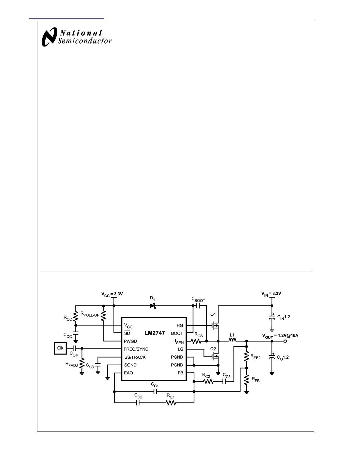
Typical Application
20150901
© 2006 National Semiconductor Corporation DS201509 www.national.com
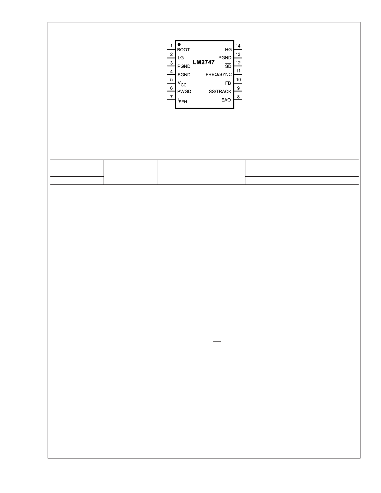
Connection Diagram
LM2747
14-Lead Plastic TSSOP
20150990
= 155˚C/W
θ
JA
NS Package Number MTC14
Ordering Information
Order Number Package Type NSC Package Drawing Supplied As
LM2747MTC
LM2747MTCX 2500 Units on Tape and Reel
Pin Description
BOOT (Pin 1) - Bootstrap pin. This is the supply rail for the
high-side gate driver. When the high-side MOSFET turns on,
the voltage on this pin should be at least one gate threshold
above the regulator input voltage V
MOSFET. See MOSFET Gate Drivers in the Application
Information section for more details on how to select MOSFETs.
LG (Pin 2) - Low-gate drive pin. This is the gate drive for the
low-side N-channel MOSFET. This signal is interlocked with
the high-side gate drive HG (Pin 14), so as to avoid shootthrough.
PGND (Pins 3, 13) - Power ground. This is also the ground
for the low-side MOSFET driver. Both the pins must be
connected together on the PCB and form a ground plane,
which is usually also the system ground.
SGND (Pin 4) - Signal ground. It should be connected
appropriately to the ground plane with due regard to good
layout practices in switching power regulator circuits.
(Pin 5) Supply rail for the control sections of the IC.
V
CC
PWGD (Pin 6) - Power Good pin. This is an open drain
output, which is typically meant to be connected to V
any other low voltage source through a pull-up resistor.
Choose the pull-up resistor so that the current going into this
pin is kept below 1 mA. A recommended value for the pull-up
resistor is 100 kΩ for most applications. The voltage on this
pin is thus pulled low under output undervoltage or overvoltage fault conditions and also under input UVLO.
(Pin 7) - Current limit threshold setting pin. This sources
I
SEN
a fixed 40 µA current. A resistor of appropriate value should
be connected between this pin and the drain of the low-side
TSSOP-14 MTC14
to properly turn on the
IN
or
CC
EAO (Pin 8) - Output of the error amplifier. The voltage level
on this pin is compared with an internally generated ramp
signal to determine the duty cycle. This pin is necessary for
compensating the control loop.
SS/TRACK (Pin 9) - Soft-start and tracking pin. This pin is
internally connected to the non-inverting input of the error
amplifier during soft-start, and in fact any time the SS/
TRACK pin voltage happens to be below the internal reference voltage. For the basic soft-start function, a capacitor of
minimum value 1 nF is connected from this pin to ground. To
track the rising ramp of another power supply’s output, connect a resistor divider from the output of that supply to this
pin as described in Application Information.
FB (Pin 10) - Feedback pin. This is the inverting input of the
error amplifier, which is used for sensing the output voltage
and compensating the control loop.
FREQ/SYNC (Pin 11) - Frequency adjust pin. The switching
frequency is set by connecting a resistor of suitable value
between this pin and ground. Some typical values (rounded
up to the nearest standard values) are 150 kΩ for 200 kHz,
100 kΩ for 300 kHz, 51.1 kΩ for 500 kHz, 18.7 kΩ for 1 MHz.
This pin is also used to synchronize to an external clock
within the range of 250kHz to 1MHz.
SD (Pin 12) - IC shutdown pin. Pull this pin to V
the IC is enabled. Connect to ground to disable the IC. Under
shutdown, both high-side and low-side drives are off. This
pin also features a precision threshold for power supply
sequencing purposes, as well as a low threshold to ensure
minimal quiescent current.
HG (Pin 14) - High-gate drive pin. This is the gate drive for
the high-side N-channel MOSFET. This signal is interlocked
with LG (Pin 2) to avoid shoot-through.
MOSFET (switch node). The minimum value for this resistor
is1kΩ.
94 Units on Rail
to ensure
CC
www.national.com 2
LM2747
Absolute Maximum Ratings (Note 1)
If Military/Aerospace specified devices are required,
please contact the National Semiconductor Sales Office/
Distributors for availability and specifications.
V
CC
BOOT Voltage -0.3 to 18V
I
SEN
FREQ/SYNC Voltage -0.5 to V
All other pins -0.3 to V
Junction Temperature 150˚C
Storage Temperature −65˚C to 150˚C
-0.3 to 7V
-0.3 to 14V
+ 0.3V
CC
+ 0.3V
CC
Soldering Information
Lead Temperature (soldering, 10sec) 260˚C
Infrared or Convection (20sec) 235˚C
ESD Rating (Note 3) 2kV
Operating Ratings
Supply Voltage Range, VCC(Note 2) 3V to 6V
BOOT Voltage Range 1V to 17V
Junction Temperature Range (T
Thermal Resistance (θ
) 155˚C/W
JA
) −40˚C to +125˚C
J
Electrical Characteristics
VCC= 3.3V unless otherwise indicated. Typicals and limits appearing in plain type apply for TA=TJ= 25˚C. Limits appearing in
boldface type apply over full Operating Temperature Range. Datasheet min/max specification limits are guaranteed by design,
test, or statistical analysis.
Symbol Parameter Conditions Min Typ Max Units
V
FB
V
ON
I
Q_VCC
t
PWGD1
t
PWGD2
I
SS-ON
I
SS-OC
I
SEN-TH
I
FB
ERROR AMPLIFIER
GBW Error Amplifier Unity Gain
G Error Amplifier DC Gain 118 dB
SR Error Amplifier Slew Rate 2 V/µs
I
EAO
V
EAO
FB Pin Voltage VCC=3Vto6V 0.594 0.6 0.606 V
UVLO Thresholds VCCRising
Falling
V
CC
V
= 3.3V, VSD= 3.3V
CC
= 600 kHz
f
Operating VCCCurrent
Shutdown V
Current VCC= 3.3V, VSD=0V 1 3 µA
CC
SW
V
= 5V, VSD= 3.3V
CC
= 600 kHz
f
SW
1.1 1.7 2.3
1.3 2 2.6
2.79
2.42
PWGD Pin Response Time VFBRising 10 µs
PWGD Pin Response Time VFBFalling 10 µs
SS Pin Source Current VSS=0V 7 10 14 µA
SS Pin Sink Current During Over
Current
I
Pin Source Current Trip
SEN
Point
VSS= 2.0V
90 µA
25 40 55 µA
FB Pin Current Sourcing 20 nA
Bandwidth
EAO Pin Current Sourcing and
Sinking Capability
9 MHz
14
16
Error Amplifier Output Voltage Minimum 1 V
Maximum 2.2 V
V
mA
mA
www.national.com3
Electrical Characteristics (Continued)
VCC= 3.3V unless otherwise indicated. Typicals and limits appearing in plain type apply for TA=TJ= 25˚C. Limits appearing in
LM2747
boldface type apply over full Operating Temperature Range. Datasheet min/max specification limits are guaranteed by design,
test, or statistical analysis.
Symbol Parameter Conditions Min Typ Max Units
GATE DRIVE
I
Q-BOOT
R
HG_UP
BOOT Pin Quiescent Current V
High-Side MOSFET Driver
Pull-Up ON resistance
R
HG_DN
High-Side MOSFET Driver
Pull-Down ON resistance
R
LG_UP
Low-Side MOSFET Driver Pull-Up
ON resistance
R
LG_DN
Low-Side MOSFET Driver
Pull-Down ON resistance
OSCILLATOR
PWM Frequency
f
SW
External Synchronizing Signal
Frequency
SYNC
SYNC
D
MAX
Synchronization Signal Low
L
Threshold
Synchronization Signal High
H
Threshold
Max High-Side Duty Cycle fSW= 300 kHz
LOGIC INPUTS AND OUTPUTS
V
STBY-IH
V
STBY-IL
V
SD-IH
V
SD-IL
V
PWGD-TH-LO
V
PWGD-TH-HI
V
PWGD-HYS
Note 1: Absolute maximum ratings indicate limits beyond which damage to the device may occur. Operating ratings indicate conditions for which the device
operates correctly. Operating Ratings do not imply guaranteed performance limits.
Note 2: The power MOSFETs can run on a separate 1V to 14V rail (Input voltage, V
See the MOSFET GATE DRIVERS section under Application Information for further details.
Note 3: ESD using the human body model which is a 100pF capacitor discharged through a 1.5 kΩ resistor into each pin.
Standby High Trip Point VFB= 0.575V, V
Standby Low Trip Point VFB= 0.575V, V
SD Pin Logic High Trip Point VSDRising 1.3 V
SD Pin Logic Low Trip Point VSDFalling 0.8 V
PWGD Pin Trip Points VFBFalling 0.408 0.434 0.457 V
PWGD Pin Trip Points VFBRising 0.677 0.710 0.742 V
PWGD Hysteresis VFBFalling
= 12V, VSD=0 18 90 µA
BOOT
=5V@350 mA Sourcing 2.7 Ω
V
BOOT
350 mA Sinking 0.8 Ω
=5V@350 mA Sourcing 2.7 Ω
V
BOOT
350 mA Sinking 0.8 Ω
= 750 kΩ 50
R
FADJ
R
= 100 kΩ 300
FADJ
R
= 42.2 kΩ 475 600 725
FADJ
R
= 18.7 kΩ 1000
FADJ
Voltage Swing = 0V to V
= 250 kHz to 1 MHz 1 V
f
SW
= 250 kHz to 1 MHz 2 V
f
SW
CC
250 1000
86
= 600 kHz
f
SW
f
SW
V
SD
V
SD
= 1 MHz
Rising
Falling
BOOT
BOOT
= 3.3V
= 3.3V
0.232
78
67
60
Rising
V
FB
). Practical lower limit of VINdepends on selection of the external MOSFET.
IN
90
1.1
kHz
%
V
V
mV
www.national.com 4

Typical Performance Characteristics
LM2747
Efficiency (V
= 3.3V, fSW= 1 MHz Internal Reference Voltage vs Temperature
V
CC
OUT
= 1.2V)
20150940 20150958
Frequency vs Temperature Output Voltage vs Output Current
Switch Waveforms
= 3.3V, VIN= 5V, V
V
CC
= 3A, CSS= 12 nF, fSW= 1 MHz
I
OUT
OUT
20150960 20150956
Start-Up (Full-Load)
= 1.2V
20150946
V
= 3.3V, VIN= 5V, V
CC
= 3A, CSS= 12 nF, fSW= 1 MHz
I
OUT
OUT
= 1.2V
20150948
www.national.com5

Typical Performance Characteristics (Continued)
LM2747
Start-Up (No-Load)
V
= 3.3V, VIN= 5V, V
CC
= 12 nF, fSW= 1 MHz
C
SS
Load Transient Response
= 3.3V, VIN= 14V, V
V
CC
f
SW
= 1 MHz
OUT
OUT
Shutdown (Full-Load)
= 1.2V
20150949 20150950
= 1.2V
V
= 3.3V, VIN= 5V, V
CC
= 3A, CSS= 12 nF, fSW= 1 MHz
I
OUT
Line Transient Response (V
= 3.3V, V
V
CC
= 2A, fSW= 1 MHz
I
OUT
OUT
OUT
IN
= 1.2V
= 1.2V
=3Vto9V)
20150953 20150954
Frequency vs. Frequency Adjust Resistor
20150955
www.national.com 6
Maximum Duty Cycle vs Frequency
VCC= 3.3V
20150992

Typical Performance Characteristics (Continued)
LM2747
Maximum Duty Cycle vs V
fSW= 600 kHz
CC
Maximum Duty Cycle vs V
fSW= 1 MHz
20150993 20150994
CC
www.national.com7

Block Diagram
LM2747
Application Information
The LM2747 is a voltage-mode, high-speed synchronous
buck regulator with a PWM control scheme. It is designed for
use in set-top boxes, thin clients, DSL/Cable modems, and
other applications that require high efficiency buck converters. It has output shutdown (SD), input undervoltage lock-out
(UVLO) mode and power good (PWGD) flag (based on
overvoltage and undervoltage detection). The overvoltage
and undervoltage signals are OR-gated to drive the power
good signal and provide a logic signal to the system if the
output voltage goes out of regulation. Current limit is
achieved by sensing the voltage V
MOSFET. The LM2747 is also able to start-up with the
output pre-biased with a load and allows for the switching
frequency to be synchronized with an external clock source.
START UP/SOFT-START
When V
exceeds 2.79V and the shutdown pin (SD) sees
CC
a logic high, the soft-start period begins. Then an internal,
fixed 10 µA source begins charging the soft-start capacitor.
During soft-start the voltage on the soft-start capacitor C
connected internally to the non-inverting input of the error
amplifier. The soft-start period lasts until the voltage on the
soft-start capacitor exceeds the LM2747 reference voltage
of 0.6V. At this point the reference voltage takes over at the
non-inverting error amplifier input. The capacitance of C
determines the length of the soft-start period, and can be
approximated by:
across the low side
DS
SS
SS
20150903
Where CSSis in µF and tSSis in ms.
During soft start the Power Good flag is forced low and it is
released when the FB pin voltage reaches 70% of 0.6V. At
this point the chip enters normal operation mode, and the
output overvoltage and undervoltage monitoring starts.
SETTING THE OUTPUT VOLTAGE
The LM2747 regulates the output voltage by controlling the
duty cycle of the high side and low side MOSFETs (see
Typical Application Circuit).The equation governing output
voltage is:
is
SETTING THE SWITCHING FREQUENCY
During fixed-frequency mode of operation the PWM fre-
quency is adjustable between 50 kHz and 1 MHz and is set
by an external resistor, R
, between the FREQ/SYNC pin
FADJ
and ground. The resistance needed for a desired frequency
www.national.com 8

Application Information (Continued)
is approximated by the curve FREQUENCY vs. FREQUENCY ADJUST RESISTOR in the Typical Performance
Characteristics section.
When it is desired to synchronize the switching frequency
with an external clock source, the LM2747 has the unique
ability to synchronize from this external source within the
range of 250 kHz to 1 MHz. The external clock signal should
be AC coupled to the FREQ/SYNC pin as shown below in
Figure 1, where the R
quency is approximately within
chronizing clock frequency. An internal protection diode
clamps the low level of the synchronizing signal to approximately -0.5V. The internal clock synchrinizes to the rising
edge of the external clock.
is chosen so that the fixed fre-
FADJ
±
30% of the external syn-
switching cycle. Figure 2 shows the SW node, HG, and LG
signals during pre-bias startup. The pre-biased output voltage should not exceed V
CC+VGS
of the external High-Side
MOSFET to ensure that the High-Side MOSFET will be able
to switch during startup.
LM2747
20150989
FIGURE 1. AC Coupled Clock
It is recommended to choose an AC coupling capacitance in
the range of 50 pF to 100 pF. Exceeding the recommended
capacitance may inject excessive energy through the internal clamping diode structure present on the FREQ/SYNC
pin.
The typical trip level of the synchronization pin is 1.5V. To
ensure proper synchronization and to avoid damaging the
IC, the peak-to-peak value (amplitude) should be between
2.5V and V
. The minimum width of this pulse must be
CC
greater than 100 ns, and it’s maximum width must be 100ns
less than the period of the switching cycle.
The external clock synchronization process begins once the
LM2747 is enabled and an external clock signal is detected.
During the external clock synchronization process the internal clock initially switches at approximately 1.5 MHz and
decreases until it has matched the external clock’s frequency. The lock-in period is approximately 30 µs if the
external clock is switching at 1 MHz, and about 100 µs if the
external clock is at 200 kHz. When there is no clock signal
present, the LM2747 enters into fixed-frequency mode and
begins switching at the frequency set by the R
FADJ
resistor.
If the external clock signal is removed after frequency synchronization, the LM2747 will enter fixed-frequency mode
within two clock cycles. If the external clock is removed
within the 30 µs lock-in period, the LM2747 will re-enter
fixed-frequency mode within two internal clock cycles after
the lock-in period.
20150991
FIGURE 2. Output Pre-Bias Mode Waveforms
TRACKING A VOLTAGE LEVEL
The LM2747 can track the output of a master power supply
during soft-start by connecting a resistor divider to the SS/
TRACK pin. In this way, the output voltage slew rate of the
LM2747 will be controlled by the master supply for loads that
require precise sequencing. When the tracking function is
used no soft-start capacitor should be connected to the
SS/TRACK pin. However in all other cases, a C
value of at
SS
least 1 nF between the soft-start pin and ground should be
used.
OUTPUT PRE-BIAS STARTUP
If there is a pre-biased load on the output of the LM2747
during startup, the IC will disable switching of the low-side
MOSFET and monitor the SW node voltage during the offtime of the high-side MOSFET. There is no load current
sensing while in pre-bias mode because the low-side MOSFET never turns on. The IC will remain in this pre-bias mode
until it sees the SW node stays below 0V during the entire
high-side MOSFET’s off-time. Once it is determined that the
SW node remained below 0V during the high-side off-time,
the low-side MOSFET begins switching during the next
20150907
FIGURE 3. Tracking Circuit
One way to use the tracking feature is to design the tracking
resistor divider so that the master supply’s output voltage
) and the LM2747’s output voltage (represented sym-
(V
OUT1
bolically in Figure 3 as V
, i.e. without explicitly showing
OUT2
the power components) both rise together and reach their
www.national.com9

Application Information (Continued)
target values at the same time. For this case, the equation
LM2747
governing the values of the tracking divider resistors R
is:
R
T2
The current through RT1should be about 4 mA for precise
tracking. The final voltage of the SS/TRACK pin should be
set higher than the feedback voltage of 0.6V (say about
0.65V as in the above equation). If the master supply voltage
was 5V and the LM2747 output voltage was 1.8V, for example, then the value of R
identical soft-start times would be 150Ω. A timing diagram for
the equal soft-start time case is shown in Figure 4.
needed to give the two supplies
T1
and
T1
20150910
FIGURE 5. Tracking with Equal Slew Rates
SEQUENCING
The start up/soft-start of the LM2747 can be delayed for the
purpose of sequencing by connecting a resistor divider from
the output of a master power supply to the SD pin, as shown
in Figure 6.
20150908
FIGURE 4. Tracking with Equal Soft-Start Time
TRACKING A VOLTAGE SLEW RATE
The tracking feature can alternatively be used not to make
both rails reach regulation at the same time but rather to
have similar rise rates (in terms of output dV/dt). This
method ensures that the output voltage of the LM2747 always reaches regulation before the output voltage of the
master supply. In this case, the tracking resistors can be
determined based on the following equation:
For the example case of V
set to 150Ω as before, RT2is calculated from the above
R
T1
OUT1
= 5V and V
OUT2
= 1.8V, with
equation to be 265Ω. A timing diagram for the case of equal
slew rates is shown in Figure 5.
20150914
FIGURE 6. Sequencing Circuit
A desired delay time t
between the startup of the
DELAY
master supply output voltage and the LM2747 output voltage
can be set based on the SD pin low-to-high threshold V
SD-IH
and the slew rate of the voltage at the SD pin, SRSD:
t
DELAY=VSD-IH
/SR
SD
Note again, that in Figure 6, the LM2747’s output voltage
has been represented symbolically as V
, i.e. without
OUT2
explicitly showing the power components.
is typically 1.08V and SRSDis the slew rate of the SD
V
SD-IH
pin voltage. The values of the sequencing divider resistors
and RS2set the SRSDbased on the master supply
R
S1
output voltage slew rate, SR
, using the following equa-
OUT1
tion:
www.national.com 10

Application Information (Continued)
For example, if the master supply output voltage slew rate
was 1V/ms and the desired delay time between the startup
of the master supply and LM2747 output voltage was 5 ms,
then the desired SD pin slew rate would be (1.08V/5 ms) =
0.216V/ms. Due to the internal impedance of the SD pin, the
maximum recommended value for RS2is1kΩ. To achieve
the desired slew rate, R
diagram for this example is shown in Figure 7.
FIGURE 7. Delay for Sequencing
SD PIN IMPEDANCE
When connecting a resistor divider to the SD pin of the
LM2747 some care has to be taken. Once the SD voltage
goes above V
, a 17 µA pull-up current is activated as
SD-IH
shown in Figure 8. This current is used to create the internal
hysteresis ()170 mV); however, high external impedances
will affect the SD pin logic thresholds as well. The external
impedance used for the sequencing divider network should
preferably be a small fraction of the impedance of the SD pin
for good performance (around 1 kΩ).
would then be 274Ω. A timing
S1
20150911
20150906
FIGURE 8. SD Pin Logic
MOSFET GATE DRIVERS
The LM2747 has two gate drivers designed for driving
N-channel MOSFETs in a synchronous mode. Note that
unlike most other synchronous controllers, the bootstrap
capacitor of the LM2747 provides power not only to the
driver of the upper MOSFET, but the lower MOSFET driver
too (both drivers are ground referenced, i.e. no floating
driver).
Two things must be kept in mind here. First, the BOOT pin
has an absolute maximum rating of 18V. This must never be
exceeded, even momentarily. Since the bootstrap capacitor
is connected to the SW node, the peak voltage impressed on
the BOOT pin is the sum of the input voltage (V
) plus the
IN
voltage across the bootstrap capacitor (ignoring any forward
drop across the bootstrap diode). The bootstrap capacitor is
charged up by a given rail (called V
BOOT_DC
here) whenever
the upper MOSFET turns off. This rail can be the same as
or it can be any external ground-referenced DC rail. But
V
CC
care has to be exercised when choosing this bootstrap DC
rail that the BOOT pin is not damaged. For example, if the
desired maximum V
the same as V
, then clearly if the VCCrail is 6V, the peak
CC
is 14V, and V
IN
BOOT_DC
is chosen to be
voltage on the BOOT pin is 14V + 6V = 20V. This is unacceptable, as it is in excess of the rating of the BOOT pin. A
of 3V would be acceptable in this case. Or the VINrange
V
CC
must be reduced accordingly. There is also the option of
deriving the bootstrap DC rail from another 3V external rail,
independent of V
.
CC
The second thing to be kept in mind here is that the output of
the low-side driver swings between the bootstrap DC rail
level of V
BOOT_DC
high-side driver swings between V
and Ground, whereas the output of the
+V
IN
BOOT_DC
and
Ground. To keep the high-side MOSFET fully on when desired, the Gate pin voltage of the MOSFET must be higher
than its instantaneous Source pin voltage by an amount
equal to the ’Miller plateau’. It can be shown that this plateau
is equal to the threshold voltage of the chosen MOSFET plus
a small amount equal to Io/g. Here Io is the maximum load
current of the application, and g is the transconductance of
this MOSFET (typically about 100 for logic-level devices).
That means we must choose V
BOOT_DC
to at least exceed
LM2747
www.national.com11

Application Information (Continued)
the Miller plateau level. This may therefore affect the choice
LM2747
of the threshold voltage of the external MOSFETs, and that
in turn may depend on the chosen V
So far, in the discussion above, the forward drop across the
bootstrap diode has been ignored. But since that does affect
the output of the driver somewhat, it is a good idea to include
this drop in the following examples. Looking at the Typical
Application schematic, this means that the difference voltage
V
CC-VD1
, which is the voltage the bootstrap capacitor
charges up to, must always be greater than the maximum
tolerance limit of the threshold voltage of the upper MOSFET. Here V
is the forward voltage drop across the boot-
D1
strap diode D1. This may place restrictions on the minimum
input voltage and/or type of MOSFET used.
A basic bootstrap circuit can be built using one Schottky
diode and a small capacitor, as shown in Figure 9. The
capacitor C
serves to maintain enough voltage between
BOOT
the top MOSFET gate and source to control the device even
when the top MOSFET is on and its source has risen up to
the input voltage level. The charge pump circuitry is fed from
, which can operate over a range from 3.0V to 6.0V.
V
CC
Using this basic method the voltage applied to the gates of
both high-side and low-side MOSFETs is V
method works well when V
CC
drives will get at least 4.0V of drive voltage during the worst
case of V
CC-MIN
= 4.5V and V
MOSFETs generally specify their on-resistance at V
4.5V. When V
= 3.3V±10%, the gate drive at worst case
CC
could go as low as 2.5V. Logic level MOSFETs are not
guaranteed to turn on, or may have much higher onresistance at 2.5V. Sub-logic level MOSFETs, usually specified at V
= 2.5V, will work, but are more expensive, and
GS
tend to have higher on-resistance. The circuit in Figure 9
works well for input voltages ranging from 1V up to 14V and
=5V±10%, because the drive voltage depends only on
V
CC
.
V
CC
BOOT_DC
is 5V±10%, because the gate
= 0.5V. Logic level
D-MAX
rail.
CC-VD
. This
GS
powers both the V
and the bootstrap circuit, providing
CC
efficient drive for logic level MOSFETs. An example of this
circuit is shown in Figure 10.
20150913
FIGURE 10. LM78L05 Feeding Basic Charge Pump
=
Figure 11 shows a second possibility for bootstrapping the
MOSFET drives using a doubler. This circuit provides an
equal voltage drive of V
-3VD+VINto both the high-side
CC
and low-side MOSFET drives. This method should only be
used in circuits that use 3.3V for both V
V
IN=VCC
= 3.0V (10% lower tolerance on 3.3V) and VD=
and VIN. Even with
CC
0.5V both high-side and low-side gates will have at least
4.5V of drive. The power dissipation of the gate drive circuitry is directly proportional to gate drive voltage, hence the
thermal limits of the LM2747 IC will quickly be reached if this
circuit is used with V
or VINvoltages over 5V.
CC
20150912
FIGURE 9. Basic Charge Pump (Bootstrap)
Note that the LM2747 can be paired with a low cost linear
regulator like the LM78L05 to run from a single input rail
between 6.0 and 14V. The 5V output of the linear regulator
www.national.com 12
20150919
FIGURE 11. Charge Pump with Added Gate Drive
All the gate drive circuits shown in the above figures typically
use 100 nF ceramic capacitors in the bootstrap locations.

Application Information (Continued)
POWER GOOD SIGNAL
The open drain output on the Power Good pin needs a
pull-up resistor to a low voltage source. The pull-up resistor
should be chosen so that the current going into the Power
Good pin is less than 1 mA. A 100 kΩ resistor is recommended for most applications.
The Power Good signal is an OR-gated flag which takes into
account both output overvoltage and undervoltage conditions. If the feedback pin (FB) voltage is 18% above its
nominal value (118% x V
value (72% x V
= 0.42V) the Power Good flag goes low.
FB
The Power Good flag can be used to signal other circuits that
the output voltage has fallen out of regulation, however the
switching of the LM2747 continues regardless of the state of
the Power Good signal. The Power Good flag will return to
logic high whenever the feedback pin voltage is between
72% and 118% of 0.6V.
UVLO
The 2.79V turn-on threshold on V
of about 300 mV. If V
nitely enters UVLO mode. UVLO consists of turning off the
top and bottom MOSFETS and remaining in that condition
until V
rises above 2.79V. As with normal shutdown initi-
CC
ated by the SD pin, the soft-start capacitor is discharged
through an internal MOSFET, ensuring that the next start-up
will be controlled by the soft-start circuitry.
= 0.708V) or falls 28% below that
FB
has a built in hysteresis
CC
drops below 2.42V, the chip defi-
CC
LM2747
on. (The point of peak inductor current, see Figure 12). Note
that in normal operation mode the high-side MOSFET always turns on at the beginning of a clock cycle. In current
limit mode, by contrast, the high-side MOSFET on-pulse is
skipped. This causes inductor current to fall. Unlike a normal
operation switching cycle, however, in a current limit mode
switching cycle the high-side MOSFET will turn on as soon
as inductor current has fallen to the current limit threshold.
The LM2747 will continue to skip high-side MOSFET pulses
until the inductor current peak is below the current limit
threshold, at which point the system resumes normal operation.
CURRENT LIMIT
Current limit is realized by sensing the voltage across the
low-side MOSFET while it is on. The R
of the MOSFET
DSON
is a known value; hence the current through the MOSFET
can be determined as:
V
DS=IOUTxRDSON
The current through the low-side MOSFET while it is on is
also the falling portion of the inductor current. The current
limit threshold is determined by an external resistor, R
connected between the switching node and the I
constant current (I
, causing a fixed voltage drop. This fixed voltage is
R
CS
compared against V
) of 40 µA typical is forced through
SEN-TH
and if the latter is higher, the current
DS
SEN
CS
pin. A
limit of the chip has been reached. To obtain a more accurate
value for R
R
DSON
you must consider the operating values of
CS
and I
at their operating temperatures in your
SEN-TH
application and the effect of slight parameter differences
from part to part. R
equation using the R
can be found by using the following
CS
value of the low side MOSFET at
DSON
it’s expected hot temperature and the absolute minimum
value expected over the full temperature range for the for the
which is 25 µA:
I
SEN-TH
R
CS=RDSON-HOTxILIM/ISEN-TH
For example, a conservative 15A current limit in a 10A
design with a R
DSON-HOT
resistor. The minimum value for R
of 10 mΩ would requirea6kΩ
in any application is 1
CS
kΩ. Because current sensing is done across the low-side
MOSFET, no minimum high-side on-time is necessary. The
LM2747 enters current limit mode if the inductor current
exceeds the current limit threshold at the point where the
high-side MOSFET turns off and the low-side MOSFET turns
20150988
FIGURE 12. Current Limit Threshold
Unlike a high-side MOSFET current sensing scheme, which
limits the peaks of inductor current, low-side current sensing
is only allowed to limit the current during the converter
off-time, when inductor current is falling. Therefore in a typi-
,
cal current limit plot the valleys are normally well defined, but
the peaks are variable, according to the duty cycle. The
PWM error amplifier and comparator control the off-pulse of
the high-side MOSFET, even during current limit mode,
meaning that peak inductor current can exceed the current
limit threshold. Assuming that the output inductor does not
saturate, the maximum peak inductor current during current
limit mode can be calculated with the following equation:
Where TSWis the inverse of switching frequency fSW. The
200 ns term represents the minimum off-time of the duty
cycle, which ensures enough time for correct operation of
the current sensing circuitry.
In order to minimize the time period in which peak inductor
current exceeds the current limit threshold, the IC also discharges the soft-start capacitor through a fixed 90 µA sink.
The output of the LM2747 internal error amplifier is limited by
the voltage on the soft-start capacitor. Hence, discharging
the soft-start capacitor reduces the maximum duty cycle D of
the controller. During severe current limit this reduction in
duty cycle will reduce the output voltage if the current limit
conditions last for an extended time. Output inductor current
www.national.com13

Application Information (Continued)
will be reduced in turn to a flat level equal to the current limit
LM2747
threshold. The third benefit of the soft-start capacitor discharge is a smooth, controlled ramp of output voltage when
the current limit condition is cleared.
SHUTDOWN
If the shutdown pin is pulled low, (below 0.8V) the LM2747
enters shutdown mode, and discharges the soft-start capacitor through a MOSFET switch. The high and low-side MOSFETs are turned off. The LM2747 remains in this state as
long as V
istics table). To assure proper IC start-up the shutdown pin
should not be left floating. For normal operation this pin
should be connected directly to V
between 1.3V to V
table).
DESIGN CONSIDERATIONS
The following is a design procedure for all the components
needed to create the Typical Application Circuit shown on
the front page. This design converts 3.3V (V
(V
OUT
and a switching frequency of 300 kHz. The same procedures
can be followed to create many other designs with varying
input voltages, output voltages, and load currents.
Input Capacitor
The input capacitors in a Buck converter are subjected to
high stress due to the input current trapezoidal waveform.
Input capacitors are selected for their ripple current capability and their ability to withstand the heat generated since that
ripple current passes through their ESR. Input rms ripple
current is approximately:
Where duty cycleD=V
The power dissipated by each input capacitor is:
where n is the number of paralleled capacitors, and ESR is
the equivalent series resistance of each capacitor. The equation above indicates that power loss in each capacitor decreases rapidly as the number of input capacitors increases.
The worst-case ripple for a Buck converter occurs during full
load and when the duty cycle (D) is 0.5. For this 3.3V to 1.2V
design the duty cycle is 0.364. For a 4A maximum load the
ripple current is 1.92A.
Output Inductor
The output inductor forms the first half of the power stage in
a Buck converter. It is responsible for smoothing the square
wave created by the switching action and for controlling the
output current ripple (∆I
selecting between tradeoffs in efficiency and response time.
The smaller the output inductor, the more quickly the converter can respond to transients in the load current. However, as shown in the efficiency calculations, a smaller inductor requires a higher switching frequency to maintain the
same level of output current ripple. An increase in frequency
sees a logic low (see the Electrical Character-
SD
or to another voltage
(see the Electrical Characteristics
CC
CC
) at a maximum load of 4A with an efficiency of 89%
.
OUT/VIN
). The inductance is chosen by
OUT
) to 1.2V
IN
can mean increasing loss in the MOSFETs due to the charging and discharging of the gates. Generally the switching
frequency is chosen so that conduction loss outweighs
switching loss. The equation for output inductor selection is:
L = 1.6 µH
Here we have plugged in the values for output current ripple,
input voltage, output voltage, switching frequency, and assumed a 40% peak-to-peak output current ripple. This yields
an inductance of 1.6 µH. The output inductor must be rated
to handle the peak current (also equal to the peak switch
current), which is (I
OUT
+ (0.5 x ∆I
)) = 4.8A, for a 4A
OUT
design.
The Coilcraft DO3316P-222P is 2.2 µH, is rated to 7.4A
peak, and has a direct current resistance (DCR) of 12 mΩ.
After selecting the Coilcraft DO3316P-222P for the output
inductor, actual inductor current ripple should be recalculated with the selected inductance value, as this information is needed to select the output capacitor. Rearranging the equation used to select inductance yields the
following:
V
voltage, or 3.6V at V
is assumed to be 10% above the steady state input
IN(MAX)
= 3.3V. The re-calculated current
IN
ripple will then be 1.2A. This gives a peak inductor/switch
current will be 4.6A.
Output Capacitor
The output capacitor forms the second half of the power
stage of a Buck switching converter. It is used to control the
output voltage ripple (∆V
) and to supply load current
OUT
during fast load transients.
In this example the output current is 4A and the expected
type of capacitor is an aluminum electrolytic, as with the
input capacitors. Other possibilities include ceramic, tantalum, and solid electrolyte capacitors, however the ceramic
type often do not have the large capacitance needed to
supply current for load transients, and tantalums tend to be
more expensive than aluminum electrolytic. Aluminum capacitors tend to have very high capacitance and fairly low
ESR, meaning that the ESR zero, which affects system
stability, will be much lower than the switching frequency.
The large capacitance means that at the switching frequency, the ESR is dominant, hence the type and number of
output capacitors is selected on the basis of ESR. One
simple formula to find the maximum ESR based on the
desired output voltage ripple, ∆V
put current ripple, ∆I
OUT
, is:
and the designed out-
OUT
www.national.com 14

Application Information (Continued)
In this example, in order to maintain a 2% peak-to-peak
output voltage ripple and a 40% peak-to-peak inductor current ripple, the required maximum ESR is 20 mΩ. The Sanyo
4SP560M electrolytic capacitor will give an equivalent ESR
of 14 mΩ. The capacitance of 560 µF is enough to supply
energy even to meet severe load transient demands.
MOSFETs
Selection of the power MOSFETs is governed by a trade-off
between cost, size, and efficiency. One method is to determine the maximum cost that can be endured, and then
select the most efficient device that fits that price. Breaking
down the losses in the high-side and low-side MOSFETs and
then creating spreadsheets is one way to determine relative
efficiencies between different MOSFETs. Good correlation
between the prediction and the bench result is not guaranteed, however. Single-channel buck regulators that use a
controller IC and discrete MOSFETs tend to be most efficient
for output currents of 2 to 10A.
Losses in the high-side MOSFET can be broken down into
conduction loss, gate charging loss, and switching loss.
Conduction, or I
In the above equations the factor 1.3 accounts for the increase in MOSFET R
1.3 can be ignored and the R
using the R
datasheets.
Gate charging loss results from the current driving the gate
capacitance of the power MOSFETs, and is approximated
as:
where ‘n’ is the number of MOSFETs (if multiple devices
have been placed in parallel), V
MOSFET Gate Drivers section) and Q
of the MOSFET. If different types of MOSFETs are used, the
‘n’ term can be ignored and their gate charges simply
summed to form a cumulative Q
from conduction and switching losses in that the actual
dissipation occurs in the LM2747, and not in the MOSFET
itself.
Switching loss occurs during the brief transition period as the
high-side MOSFET turns on and off, during which both current and voltage are present in the channel of the MOSFET.
It can be approximated as:
where trand tfare the rise and fall times of the MOSFET.
Switching loss occurs in the high-side MOSFET only.
For this example, the maximum drain-to-source voltage applied to either MOSFET is 3.6V. The maximum drive voltage
at the gate of the high-side MOSFET is 3.1V, and the maximum drive voltage for the low-side MOSFET is 3.3V. Due to
the low drive voltages in this example, a MOSFET that turns
on fully with 3.1V of gate drive is needed. For designs of 5A
and under, dual MOSFETs in SO-8 provide a good trade-off
between size, cost, and efficiency.
2
R loss, is approximately:
PC=D(I
2
xR
O
DSON-HI
x 1.3)
(High-Side MOSFET)
=(1-D)x(I
P
C
2
xR
O
DSON-LO
x 1.3)
(Low-Side MOSFET)
due to heating. Alternatively, the
DSON
Vs. Temperature curves in the MOSFET
DSON
=nx(VDD)xQGxf
P
GC
=0.5xVINxIOx(tr+tf)xf
P
SW
of the MOSFET estimated
DSON
SW
is the driving voltage (see
DD
G
is the gate charge
GS
. Gate charge loss differs
SW
Support Components
C
2 - A small (0.1 to 1 µF) ceramic capacitor should be
IN
placed as close as possible to the drain of the high-side
MOSFET and source of the low-side MOSFET (dual MOSFETs make this easy). This capacitor should be X5R type
dielectric or better.
R
CC,CCC
ensure smooth DC voltage for the chip supply. R
be1to10Ω.C
C
BOOT
R
PULL-UP
- These are standard filter components designed to
should 1 µF, X5R type or better.
CC
CC
- Bootstrap capacitor, typically 100 nF.
– This is a standard pull-up resistor for the open-
should
drain power good signal (PWGD). The recommended value
is 100 kΩ connected to V
. If this feature is not necessary,
CC
the resistor can be omitted.
- A small Schottky diode should be used for the bootstrap.
D
1
It allows for a minimum drop for both high and low-side
drivers. The MBR0520 or BAT54 work well in most designs.
- Resistor used to set the current limit. Since the design
R
CS
calls for a peak current magnitude (I
OUT
+ (0.5 x ∆I
OUT
)) of
4.8A, a safe setting would be 6A. (This is below the saturation current of the output inductor, which is 7A.) Following the
equation from the Current Limit section, a 1.3 kΩ resistor
should be used.
- This resistor is used to set the switching frequency of
R
FADJ
the chip. The resistor value is approximated from the Frequency vs Frequency Adjust Resistor curve in the Typical
Performance Characteristics section. For 300 kHz operation,
a 100 kΩ resistor should be used.
- The soft-start capacitor depends on the user require-
C
SS
ments and is calculated based on the equation given in the
section titled START UP/SOFT-START. Therefore, fora7ms
delay, a 12 nF capacitor is suitable.
Control Loop Compensation
The LM2747 uses voltage-mode (‘VM’) PWM control to correct changes in output voltage due to line and load transients. VM requires careful small signal compensation of the
control loop for achieving high bandwidth and good phase
margin.
The control loop is comprised of two parts. The first is the
power stage, which consists of the duty cycle modulator,
output inductor, output capacitor, and load. The second part
is the error amplifier, which for the LM2747 isa9MHz
op-amp used in the classic inverting configuration. Figure 13
shows the regulator and control loop components.
LM2747
www.national.com15

Application Information (Continued)
LM2747
20150964
a=LCO(RO+RC)
b=L+C
c=R
O(RORL+RORC+RCRL
O+RL
)
FIGURE 13. Power Stage and Error Amp
One popular method for selecting the compensation components is to create Bode plots of gain and phase for the power
stage and error amplifier. Combined, they make the overall
bandwidth and phase margin of the regulator easy to see.
Software tools such as Excel, MathCAD, and Matlab are
useful for showing how changes in compensation or the
power stage affect system gain and phase.
The power stage modulator provides a DC gain A
DC
that is
equal to the input voltage divided by the peak-to-peak value
of the PWM ramp. This ramp is 1.0V
for the LM2747.
pk-pk
The inductor and output capacitor create a double pole at
frequency f
ate a single zero at frequency f
= 3.3V, these quantities are:
V
IN
, and the capacitor ESR and capacitance cre-
DP
. For this example, with
ESR
In the equation for fDP, the variable RLis the power stage
resistance, and represents the inductor DCR plus the on
resistance of the top power MOSFET. R
is the output
O
voltage divided by output current. The power stage transfer
function G
is given by the following equation, and Figure
PS
14 shows Bode plots of the phase and gain in this example.
20150969
20150970
FIGURE 14. Power Stage Gain and Phase
The double pole at 4.5 kHz causes the phase to drop to
approximately -130˚ at around 10 kHz. The ESR zero, at
20.3 kHz, provides a +90˚ boost that prevents the phase
from dropping to -180
o
. If this loop were left uncompensated,
the bandwidth would be approximately 10 kHz and the
phase margin 53˚. In theory, the loop would be stable, but
would suffer from poor DC regulation (due to the low DC
gain) and would be slow to respond to load transients (due to
the low bandwidth.) In practice, the loop could easily become
unstable due to tolerances in the output inductor, capacitor,
or changes in output current, or input voltage. Therefore, the
loop is compensated using the error amplifier and a few
passive components.
For this example, a Type III, or three-pole-two-zero approach
gives optimal bandwidth and phase.
In most voltage mode compensation schemes, including
Type III, a single pole is placed at the origin to boost DC gain
www.national.com 16

Application Information (Continued)
LM2747
as high as possible. Two zeroes f
and fZ2are placed at the
Z1
double pole frequency to cancel the double pole phase lag.
Then, a pole, f
A final pole f
is placed at the frequency of the ESR zero.
P1
is placed at one-half of the switching fre-
P2
quency. The gain of the error amplifier transfer function is
selected to give the best bandwidth possible without violating the Nyquist stability criteria. In practice, a good crossover
point is one-fifth of the switching frequency, or 60 kHz for this
example. The generic equation for the error amplifier transfer
function is:
In this equation the variable AEAis a ratio of the values of the
capacitance and resistance of the compensation components, arranged as shown in Figure 13.A
is selected to
EA
provide the desired bandwidth. A starting value of 80,000 for
should give a conservative bandwidth. Increasing the
A
EA
value will increase the bandwidth, but will also decrease
phase margin. Designs with 45-60˚ are usually best because
they represent a good trade-off between bandwidth and
phase margin. In general, phase margin is lowest and gain
highest (worst-case) for maximum input voltage and minimum output current. One method to select A
is to use an
EA
iterative process beginning with these worst-case conditions.
1. Increase A
EA
2. Check overall bandwidth and phase margin
3. Change V
to minimum and recheck overall bandwidth
IN
and phase margin
4. Change I
to maximum and recheck overall bandwidth
O
and phase margin
The process ends when the both bandwidth and the phase
margin are sufficiently high. For this example input voltage
can vary from 3.0 to 3.6V and output current can vary from 0
to 4A, and after a few iterations a moderate gain factor of
101dB is used.
The error amplifier of the LM2747 has a unity-gain bandwidth of 9 MHz. In order to model the effect of this limitation,
the open-loop gain can be calculated as:
20150974
20150975
FIGURE 15. Error Amp. Gain and Phase
In VM regulators, the top feedback resistor R
of the compensation. Setting R
to 10 kΩ±1%, usually
FB2
forms a part
FB2
gives values for the other compensation resistors and capacitors that fall within a reasonable range. (Capacitances
1 pF, resistances<1MΩ)CC1,CC2,CC3,RC1, and RC2are
selected to provide the poles and zeroes at the desired
frequencies, using the following equations:
>
The new error amplifier transfer function that takes into
account unity-gain bandwidth is:
The gain and phase of the error amplifier are shown in
Figure 15.
www.national.com17

Application Information (Continued)
LM2747
In practice, a good trade off between phase margin and
±
and CC2,
C1
10%
bandwidth can be obtained by selecting the closest
capacitor values above what are suggested for C
±
the closest
, and the closest±1% resistor values below the sugges-
C
C3
tions for R
10% capacitor value below the suggestion for
. Note that if the suggested value for RC2is
C1,RC2
less than 100Ω, it should be replaced by a short circuit.
Following this guideline, the compensation components will
be:
=27pF±10%, CC2= 820 pF±10%
C
C1
= 2.7 nF±10%, RC1= 39.2 kΩ±1%
C
C3
= 2.55 kΩ±1%
R
C2
The transfer function of the compensation block can be
derived by considering the compensation components as
impedance blocks Z
and ZIaround an inverting op-amp:
F
20150985
20150986
As with the generic equation, G
EA-ACTUAL
must be modified
to take into account the limited bandwidth of the error amplifier. The result is:
The total control loop transfer function H is equal to the
power stage transfer function multiplied by the error amplifier
transfer function.
H=G
PSxHEA
The bandwidth and phase margin can be read graphically
from Bode plots of H
as shown in Figure 16.
EA
FIGURE 16. Overall Loop Gain and Phase
The bandwidth of this example circuit is 59 kHz, with a phase
margin of 60˚.
EFFICIENCY CALCULATIONS
The following is a sample calculation.
A reasonable estimation of the efficiency of a switching buck
controller can be obtained by adding together the Output
Power (P
The Output Power (P
design is (1.2V x 4A) = 4.8W. The Total Power (P
) loss and the Total Power (P
OUT
) for the Typical Application Circuit
OUT
TOTAL
) loss:
TOTAL
), with
an efficiency calculation to complement the design, is shown
below.
The majority of the power losses are due to the low side and
high side MOSFET’s losses. The losses in any MOSFET are
group of switching (P
P
FET=PSW+PCND
SW
P
FET
FET Switching Loss (P
P
SW=PSW(ON)
PSW=0.5xVINxI
) and conduction losses (P
= 61.38 mW + 270.42 mW
= 331.8 mW
)
SW
+P
SW(OFF)
x(tr+tf)xf
OUT
SW
CND
).
www.national.com 18

Application Information (Continued)
P
=0.5x3.3Vx4Ax300kHzx31ns
SW
= 61.38 mW
P
SW
SW
and turn-off
r
is the
GS
The FDS6898A has a typical turn-on rise time t
fall time t
of 15 ns and 16 ns, respectively. The switching
f
losses for this type of dual N-Channel MOSFETs are
0.061W.
2
OUT
OUT
CND
xR
)
xR
DS(ON)
xkxD
DS(ON)
x k x (1-D)
of a FET due to heat-
DS(ON)
FET Conduction Loss (P
P
CND=PCND1+PCND2
P
=I
CND1
2
=I
P
CND2
R
=13mΩ and the factor is a constant value (k = 1.3)
DS(ON)
to account for the increasing R
ing.
= (4A)2x13mΩ x 1.3 x 0.364
P
CND1
= (4A)2x13mΩ x 1.3 x (1 - 0.364)
P
CND2
P
= 98.42 mW + 172 mW = 270.42 mW
CND
There are few additional losses that are taken into account:
IC Operating Loss (P
where I
is the typical operating VCCcurrent
Q-VCC
P
FET Gate Charging Loss (P
P
GATE
IC)
PIC=I
Q_VCCxVCC
= 1.7 mA x 3.3V = 5.61 mW
IC
)
GATE
=nxVCCxQGSxf
P
GATE
=2x3.3Vx3nCx300kHz
= 5.94 mW
P
GATE
,
The value n is the total number of FETs used and Q
typical gate-source charge value, which is 3 nC. For the
FDS6898A the gate charging loss is 5.94 mW.
Input Capacitor Loss (P
CAP
)
Here n is the number of paralleled capacitors, ESR is the
equivalent series resistance of each, and P
is the dissi-
CAP
pation in each. So for example if we use only one input
capacitor of 24 mΩ.
P
= 88.8 mW
CAP
IND
IND
=I
)
2
x DCR
OUT
Output Inductor Loss (P
P
where DCR is the DC resistance. Therefore, for example
P
= (4A)2x11mΩ
IND
= 176 mW
P
IND
Total System Efficiency
P
TOTAL=PFET+PIC+PGATE+PCAP+PIND
LM2747
where,
www.national.com19

Example Circuits
LM2747
FIGURE 17. 3.3V to 1.8V@2A, fSW= 300 kHz
PART PART NUMBER TYPE PACKAGE DESCRIPTION VENDOR
U1 LM2747 Synchronous
Controller
Q1 FDS6898A Dual N-MOSFET SO-8 20V, 10 mΩ
D1 MBR0520LTI Schottky Diode SOD-123
L1 DO3316P-472 Inductor 4.7 µH, 4.8Arms 18mΩCoilcraft
TSSOP-14 NSC
@
4.5V,
16nC
20150932
Fairchild
C
1 16SP100M Aluminum
IN
Electrolytic
CO1 6SP220M Aluminum
Electrolytic
C
CC,CBOOT,
VJ1206Y104KXXA Capacitor 1206 0.1 µF, 10% Vishay
CIN2, CO2
C
C3
C
SS
C
C2
C
C1
R
FB2
R
FB1
R
FADJ
R
C2
R
CS
R
CC
R
C1
R
PULL-UP
C
CLK
VJ0805Y332KXXA Capacitor 0805 3300 pF, 10% Vishay
VJ0805A123KXAA Capacitor 0805 12 nF, 10% Vishay
VJ0805A821KXAA Capacitor 0805 820 pF 10% Vishay
VJ0805A220KXAA Capacitor 0805 22 pF, 10% Vishay
CRCW08051002F Resistor 0805 10.0 kΩ 1% Vishay
CRCW08054991F Resistor 0805 4.99 kΩ1% Vishay
CRCW08051003F Resistor 0805 100 kΩ 1% Vishay
CRCW08052101F Resistor 0805 2.1 kΩ 1% Vishay
CRCW08052101F Resistor 0805 2.1 kΩ 1% Vishay
CRCW080510R0F Resistor 0805 10.0Ω 1% Vishay
CRCW08055492F Resistor 0805 54.9 kΩ 1% Vishay
CRCW08051003J Resistor 0805 100 kΩ 5% Vishay
VJ0805A560KXAA Capacitor 0805 56 pF, 10% Vishay
10mm x 6mm 100 µF, 16V,
2.89Arms
10mm x 6mm 220 µF, 6.3V
3.1Arms
Sanyo
Sanyo
www.national.com 20

Example Circuits (Continued)
FIGURE 18. 5V to 2.5V@2A, fSW= 300 kHz
LM2747
20150933
PART PART NUMBER TYPE PACKAGE DESCRIPTION VENDOR
U1 LM2747 Synchronous
TSSOP-14 NSC
Controller
Q1 FDS6898A Dual N-MOSFET SO-8 20V, 10 mΩ
@
4.5V, 16nCFairchild
D1 MBR0520LTI Schottky Diode SOD-123
L1 DO3316P-682 Inductor 6.8 µH, 4.4Arms, 27 mΩ Coilcraft
C
1 16SP100M Aluminum
IN
10mm x 6mm 100 µF, 16V, 2.89Arms Sanyo
Electrolytic
1 10SP56M Aluminum
C
O
6.3mm x 6mm 56 µF, 10V 1.7Arms Sanyo
Electrolytic
CCC,C
BOOT,
VJ1206Y104KXXA Capacitor 1206 0.1 µF, 10% Vishay
CIN2, CO2
C
C3
C
SS
C
C2
C
C1
R
FB2
R
FB1
R
FADJ
R
C2
R
CS
R
CC
R
C1
R
PULL-UP
C
CLK
VJ0805Y182KXXA Capacitor 0805 1800 pF, 10% Vishay
VJ0805A123KXAA Capacitor 0805 12 nF, 10% Vishay
VJ0805A821KXAA Capacitor 0805 820 pF 10% Vishay
VJ0805A330KXAA Capacitor 0805 33 pF, 10% Vishay
CRCW08051002F Resistor 0805 10.0 kΩ 1% Vishay
CRCW08053161F Resistor 0805 3.16 kΩ 1% Vishay
CRCW08051003F Resistor 0805 100 kΩ 1% Vishay
CRCW08051301F Resistor 0805 1.3 kΩ 1% Vishay
CRCW08052101F Resistor 0805 2.1 kΩ 1% Vishay
CRCW080510R0F Resistor 0805 10.0Ω 1% Vishay
CRCW08053322F Resistor 0805 33.2 kΩ 1% Vishay
CRCW08051003J Resistor 0805 100 kΩ 5% Vishay
VJ0805A560KXAA Capacitor 0805 56 pF, 10% Vishay
www.national.com21

Example Circuits (Continued)
LM2747
FIGURE 19. 12V to 3.3V@4A, fSW= 300kHz
PART PART NUMBER TYPE PACKAGE DESCRIPTION VENDOR
U1 LM2747 Synchronous
Controller
Q1 FDS6898A Dual N-MOSFET SO-8 20V, 10 mΩ
TSSOP-14 NSC
@
4.5V, 16nCFairchild
20150934
D1 MBR0520LTI Schottky Diode SOD-123
L1 DO3316P-332 Inductor 3.3 µH, 5.4Arms 15 mΩ Coilcraft
C
1 16SP100M Aluminum
IN
10mm x 6mm 100 µF, 16V, 2.89Arms Sanyo
Electrolytic
1 6SP220M Aluminum
C
O
10mm x 6mm 220 µF, 6.3V 3.1Arms Sanyo
Electrolytic
CCC,C
BOOT,
VJ1206Y104KXXA Capacitor 1206 0.1 µF, 10% Vishay
CIN2, CO2
C
C3
C
SS
C
C2
C
C1
R
FB2
R
FB1
R
FADJ
R
C2
R
CS
R
CC
R
C1
R
PULL-UP
C
CLK
VJ0805Y222KXXA Capacitor 0805 2200 pF, 10% Vishay
VJ0805A123KXAA Capacitor 0805 12 nF, 10% Vishay
VJ0805Y332KXXA Capacitor 0805 3300 pF 10% Vishay
VJ0805A820KXAA Capacitor 0805 82 pF, 10% Vishay
CRCW08051002F Resistor 0805 10.0 kΩ 1% Vishay
CRCW08052211F Resistor 0805 2.21 kΩ 1% Vishay
CRCW08051003F Resistor 0805 100 kΩ 1% Vishay
CRCW08052611F Resistor 0805 2.61 kΩ 1% Vishay
CRCW08054121F Resistor 0805 4.12 kΩ 1% Vishay
CRCW080510R0F Resistor 0805 10.0Ω 1% Vishay
CRCW08051272F Resistor 0805 12.7kΩ 1% Vishay
CRCW08051003J Resistor 0805 100 kΩ 5% Vishay
VJ0805A560KXAA Capacitor 0805 56 pF, 10% Vishay
www.national.com 22

Physical Dimensions inches (millimeters) unless otherwise noted
LM2747 Synchronous Buck Controller with Pre-bias Startup, and Optional Clock Synchronization
TSSOP-14
NS Package Number MTC14
National does not assume any responsibility for use of any circuitry described, no circuit patent licenses are implied and National reserves
the right at any time without notice to change said circuitry and specifications.
For the most current product information visit us at www.national.com.
LIFE SUPPORT POLICY
NATIONAL’S PRODUCTS ARE NOT AUTHORIZED FOR USE AS CRITICAL COMPONENTS IN LIFE SUPPORT DEVICES OR SYSTEMS
WITHOUT THE EXPRESS WRITTEN APPROVAL OF THE PRESIDENT AND GENERAL COUNSEL OF NATIONAL SEMICONDUCTOR
CORPORATION. As used herein:
1. Life support devices or systems are devices or systems
which, (a) are intended for surgical implant into the body, or
(b) support or sustain life, and whose failure to perform when
properly used in accordance with instructions for use
2. A critical component is any component of a life support
device or system whose failure to perform can be reasonably
expected to cause the failure of the life support device or
system, or to affect its safety or effectiveness.
provided in the labeling, can be reasonably expected to result
in a significant injury to the user.
BANNED SUBSTANCE COMPLIANCE
National Semiconductor manufactures products and uses packing materials that meet the provisions of the Customer Products
Stewardship Specification (CSP-9-111C2) and the Banned Substances and Materials of Interest Specification (CSP-9-111S2) and contain
no ‘‘Banned Substances’’ as defined in CSP-9-111S2.
Leadfree products are RoHS compliant.
National Semiconductor
Americas Customer
Support Center
Email: new.feedback@nsc.com
Tel: 1-800-272-9959
www.national.com
National Semiconductor
Europe Customer Support Center
Fax: +49 (0) 180-530 85 86
Email: europe.support@nsc.com
Deutsch Tel: +49 (0) 69 9508 6208
English Tel: +44 (0) 870 24 0 2171
Français Tel: +33 (0) 1 41 91 8790
National Semiconductor
Asia Pacific Customer
Support Center
Email: ap.support@nsc.com
National Semiconductor
Japan Customer Support Center
Fax: 81-3-5639-7507
Email: jpn.feedback@nsc.com
Tel: 81-3-5639-7560
 Loading...