

April 2004
LM2743
N-Channel FET Synchronous Buck Regulator Controller
for Conversion from 3.3V
LM2743 N-Channel FET Synchronous Buck Regulator Controller for Conversion from 3.3V
General Description
The LM2743 is a high-speed, N-Channel synchronous buck
regulator controller with a 2%, 0.6V feedback reference voltage intended to make down conversion from 3.3V to as low
as 0.6V easy. A fixed-frequency voltage-mode PWM control
architecture is used, that is adjustable from 50kHz to 2MHz
through an external resistor. This wide range of PWM frequencies gives the power supply designer the flexibility to
make tradeoffs among component size, cost, noise and
efficiency. The power MOSFETs can run on a separate 1V to
16V (Input Voltage, V
biased from a 3V to 6V (IC Input Voltage, V
power-good flag, precision shutdown threshold and soft start
features make power supply tracking and sequencing easy.
The LM2743 employs output under-voltage and over-voltage
flag, and current limit. Current limit is achieved by monitoring
the voltage drop across the on resistance of the low-side
MOSFET. The adaptive non-overlapping MOSFET gate drivers help avoid potential shoot-through problems while maintaining high efficiency. Both high-side and low-side MOSFETs are the lower cost N-Channel type, and the IC can
accept a bootstrap structure to saturate the high-side MOSFET for highest efficiency.
) (Note 2) rail while the regulator is
IN
), 2mA rail. A
CC
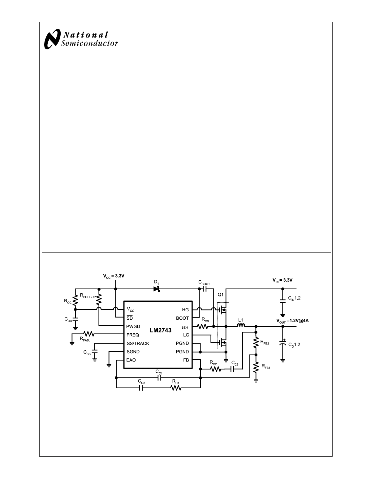
Typical Application
Features
n MOSFET input voltage (VIN) from 1V to 16V (Note 2)
n IC input voltage (V
n Output voltage adjustable down to 0.6V
n Power good flag and output enable
n Output over-voltage and under-voltage flag
n FB voltage: 2% over temperature
n Current limit without series sense resistor
n Adjustable soft start
n Tracking and sequencing with shutdown and soft start
pins
n Switching frequency from 50 kHz to 2 MHz
n TSSOP-14 package
) from 3V to 6V
CC
Applications
n 3.3V Buck Regulation
n Set-Top Boxes/ Home Gateways
n Core Logic Regulators
n High-Efficiency Buck Regulation
20095201
© 2004 National Semiconductor Corporation DS200952 www.national.com
Connection Diagram
LM2743
14-Lead Plastic TSSOP
θ
JA
NS Package Number MTC14
Pin Description
BOOT (Pin 1) - Supply rail for the N-channel MOSFET gate
drive. The voltage should be at least one gate threshold
) above the regulator input voltage (VIN) to properly
(V
GS(th)
turn on the high-side FET.
LG (Pin 2) - Gate drive for the low-side N-channel MOSFET.
This signal is interlocked with HG (Pin 14) to avoid a shootthrough problem.
PGND (Pins 3, 13) - Ground for low-side FET drive circuitry.
Connect to system ground.
SGND (Pin 4) - Ground for signal level circuitry. Connect to
system ground.
(Pin 5) Supply rail for the controller.
V
CC
PWGD (Pin 6) - Power good pin. This is an open drain
output. The pin is pulled low when the chip is in undervoltage flag (UVF), over-voltage flag (OVF), or UVLO mode.
During normal operation, this pin is connected to V
other low voltage source through a pull-up resistor (R
).
UP
(Pin 7) - Current limit threshold setting. This sources a
I
SEN
fixed 40µA current. A resistor of appropriate value should be
connected between this pin and the drain of the low-side
FET.
EAO (Pin 8) - Output of the error amplifier. The voltage level
on this pin is compared with an internally generated ramp
signal to determine the duty cycle. This pin is necessary for
compensating the control loop.
CC
PULL-
= 155˚C/W
or
20095202
SS (Pin 9) - Soft start and track pin. A 10 µA current is
sourced from this pin. This pin is connected to the noninverting input of the error amplifier during soft start, or any
time the voltage is below the reference. To track power
supplies connect a resistor divider (smaller than 10kΩ for
better precision) from the output of the master supply directly
to the SS pin. To limit the inrush current of a single power
supply, place a capacitor to ground (see Application
Information/Start Up for appropriate capacitance value). This
pin should not be forced before SD or V
(above the
CC
UVLO).
FB (Pin 10) - This is the inverting input of the error amplifier,
which is used for sensing the output voltage and compensating the control loop. The FB current is negligible.
FREQ (Pin 11) - The switching frequency (F
connecting a resistor (R
) between this pin and ground.
FADJ
) is set by
OSC
SD (Pin 12) - IC shutdown pin. To assure proper IC start-up
the SD pin should not be left floating. When this pin is pulled
low the chip turns both, high and low, sides off. While this pin
is low, the IC will not start up. This pin features a precision
threshold for power supply sequencing, as well as a lower
threshold to ensure minimal quiescent current.
HG (Pin 14) - Gate drive for the high-side N-channel MOSFET. This signal is interlocked with LG (Pin 2) to avoid a
shoot-through problem.
www.national.com 2
LM2743
Absolute Maximum Ratings (Note 1)
If Military/Aerospace specified devices are required,
please contact the National Semiconductor Sales Office/
Distributors for availability and specifications.
CC
7V
+ 0.3V
V
CC
BOOT Voltage 21V
All other pins V
Junction Temperature 150˚C
Storage Temperature −65˚C to 150˚C
Soldering Information
Lead Temperature
(soldering, 10sec) 260˚C
Infrared or Convection (20sec) 235˚C
ESD Rating (Note 3) 2 kV
Operating Ratings
IC Input Voltage (VCC) 3Vto6V
Junction Temperature Range −40˚C to +125˚C
Thermal Resistance (θ
) 155˚C/W
JA
Electrical Characteristics
VCC= 3.3V unless otherwise indicated. Typicals and limits appearing in plain type apply for TA=TJ= +25˚C. Limits appearing in
boldface type apply over full Operating Temperature Range. Datasheet min/max specification limits are guaranteed by design,
test, or statistical analysis.
Symbol Parameter Conditions Min Typ Max Units
= 3.3V 0.612 0.6 0.588
V
V
FB
V
ON
FB Pin Voltage
UVLO Thresholds Rising
Operating VCCCurrent
I
Q_VCC
Shutdown VCCCurrent
(Note 4)
t
PWGD1
t
PWGD2
I
SS-ON
I
SS-OC
PWGD Pin Response Time FB Voltage Going Up 6 µs
PWGD Pin Response Time FB Voltage Going Down 6 µs
SS Pin Source Current SS Voltage = 0V 7 10 14 µA
SS Pin Sink Current During Over
Current
I
Pin Source Current Trip
I
SEN-TH
SEN
Point
ERROR AMPLIFIER
GBW Error Amplifier Unity Gain
Bandwidth
G Error Amplifier DC Gain 106 dB
SR Error Amplifier Slew Rate 3.2 V/µs
I
EAO
EAO Pin Current Sourcing and
Sinking Capability
V
EA
Error Amplifier Maximum Swing Minimum
CC
V
=5V 0.612 0.6 0.588
CC
2.76
Falling
V
= 3.3V, SD = 3.3V
CC
Fsw = 600kHz
= 5V, SD = 3.3V
V
CC
Fsw = 600kHz
1 1.5 2.1
1 1.7 2.1
2.42
VCC= 3.3V, SD = 0V 0 110 185 µA
SS Voltage = 0V
90 µA
25 40 55 µA
9 MHz
V
= 1.5, FB = 0.55V
EAO
= 1.5, FB = 0.65V
V
EAO
2.6
9.2
0
Maximum
2
V
V
mA
mA
V
www.national.com3
Electrical Characteristics (Continued)
VCC= 3.3V unless otherwise indicated. Typicals and limits appearing in plain type apply for TA=TJ= +25˚C. Limits appearing in
LM2743
boldface type apply over full Operating Temperature Range. Datasheet min/max specification limits are guaranteed by design,
test, or statistical analysis.
Symbol Parameter Conditions Min Typ Max Units
GATE DRIVE
I
Q-BOOT
R
DS1
R
DS2
R
DS3
R
DS4
OSCILLATOR
F
OSC
D Max Duty Cycle f
LOGIC INPUTS AND OUTPUTS
V
STBY-IH
V
STBY-IL
V
SD-IH
V
SD-IL
V
PWGD-TH-LO
V
PWGD-TH-HI
V
PWGD-HYS
Note 1: Absolute maximum ratings indicate limits beyond which damage to the device may occur. Operating ratings indicate conditions for which the device
operates correctly. Opearting Ratings do not imply guaranteed performance limits.
Note 2: The power MOSFETs can run on a separate 1V to 16V rail (Input voltage, V
Note 3: The human body model is a 100pF capacitor discharged through a 1.5k resistor into each pin.
Note 4: Shutdown V
BOOT Pin Quiescent Current BOOTV = 12V, EN = 0 18 90 µA
Top FET Driver Pull-Up ON
resistance
Top FET Driver Pull-Down ON
resistance
Bottom FET Driver Pull-Up ON
BOOT-SW = 5V
@
350mA
resistance
Bottom FET Driver Pull-Down
ON resistance
R
= 813.2kΩ 50
FADJ
= 117.6kΩ 300
R
FADJ
PWM Frequency
R
= 54.4kΩ 475 600 725
FADJ
R
= 18.8kΩ 1400
FADJ
R
= 10.8kΩ 2000
FADJ
= 300kHz
PWM
= 600kHz
f
PWM
Standby High Trip Point FB = 0.575V, BOOTV = 3.3V, EN =
3 Ω
2 Ω
3 Ω
2 Ω
90
85
0.756 1.1 V
0V to 3.3V
Standby Low Trip Point FB = 0.575V, BOOTV = 3.3V, EN =
0.232 0.562
3.3V to 0V
SD Pin Logic High Trip Point FB = 0.575V, BOOTV = 3.3V, EN =
1 1.3
0V to 3.3V
SD Pin Logic Low Trip Point FB = 0.575V, BOOTV = 3.3V, EN =
0.8 1.1
3.3V to 0V
PWGD Pin Trip Points FB Voltage Going Down 0.408 0.434 0.457 V
PWGD Pin Trip Points FB Voltage Going Up 0.677 0.710 0.742 V
PWGD Hysteresis FB Voltage Going Down
FB Voltage Going Up
). Low range of VINgreatly depends on selection of the external MOSFET.
IN
current goes to zero amps after 20 seconds.
CC
60
90
kHz
%
V
V
V
mV
www.national.com 4
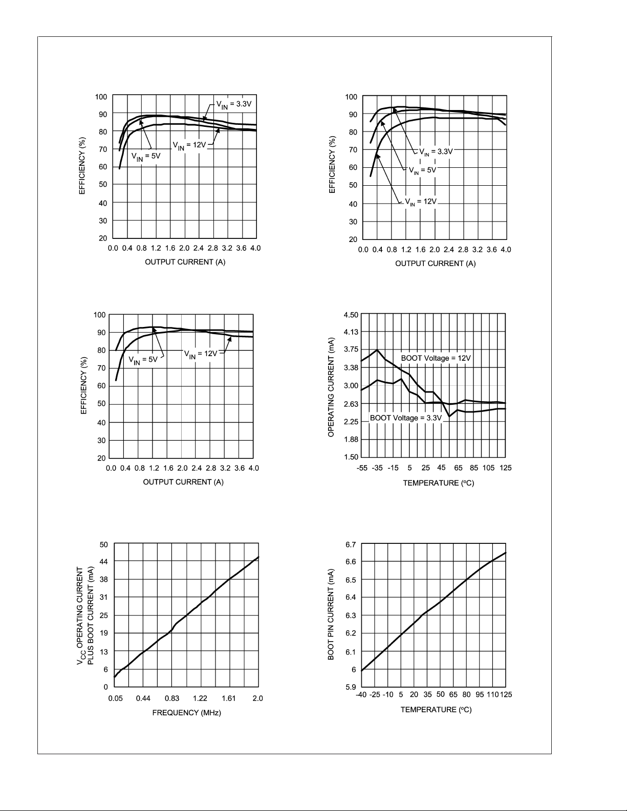
Typical Performance Characteristics
LM2743
Efficiency (V
= 3.3V, FSW= 300kHz
V
CC
Efficiency (V
= 5V, FSW= 300kHz VCCOperating Current vs Temperature
V
CC
OUT
OUT
= 1.2V)
20095240
= 3.3V)
Efficiency (V
= 3.3V, FSW= 300kHz
V
CC
OUT
= 2.5V)
20095257
20095241
VCCOperating Current plus BOOT Current vs Frequency
FDS689A FET (T
= 25˚C)
A
20095245
20095261
BOOT Pin Current vs Temperature for
BOOT Voltage = 3.3V
FSW= 300kHz, FDS689A FET, No-Load
20095242
www.national.com5

Typical Performance Characteristics (Continued)
LM2743
BOOT Pin Current vs Temperature for
BOOT Voltage = 5V
= 300kHz, FDS689A FET, No-Load
F
SW
20095243
Internal Reference Voltage vs Temperature
BOOT Pin Current vs Temperature for
BOOT Voltage = 12V
FSW= 300kHz, FDS689A FET, No-Load
20095244
R
vs Frequency
FADJ
50kHz to 2MHz, T
= 25˚C
A
20095258
Frequency vs Temperature Output Voltage vs Output Current
20095260
www.national.com 6
20095259
20095256

Typical Performance Characteristics (Continued)
LM2743
Switch Waveforms (HG Rising)
V
= 3.3V, VIN= 5V, V
CC
= 4A, CSS= 12nF, FSW= 300kHz
I
OUT
OUT
Start-Up (No-Load)
= 3.3V, VIN= 5V, V
V
CC
= 4A, CSS= 12nF, FSW= 300kHz
I
OUT
OUT
= 1.2V
20095246
= 1.2V
Switch Waveforms (HG Falling)
V
= 3.3V, VIN= 5V, V
CC
= 4A, CSS= 12nF, FSW= 300kHz
I
OUT
OUT
Start-Up (Full-Load)
V
= 3.3V, VIN= 5V, V
CC
= 4A, CSS= 12nF, FSW= 300kHz
I
OUT
OUT
= 1.2V
20095247
= 1.2V
Shutdown (Full-Load)
= 3.3V, VIN= 5V, V
V
CC
= 4A, CSS= 12nF, FSW= 300kHz
I
OUT
OUT
= 1.2V
20095248
20095250
Load Transient Response (I
= 3.3V, VIN= 5V, V
V
CC
= 12nF, FSW= 300kHz
C
SS
=0Ato4A)
OUT
= 1.2V
OUT
20095249
20095251
www.national.com7

Typical Performance Characteristics (Continued)
LM2743
Load Transient Response (I
= 3.3V, VIN= 5V, V
V
CC
= 12nF, FSW= 300kHz
C
SS
=4Ato0A)
OUT
= 1.2V
OUT
20095252
Line Transient Response (VIN=3Vto6V)
= 3.3V, V
V
CC
= 2A, FSW= 300kHz
I
OUT
OUT
= 1.2V
Load Transient Response
V
= 3.3V, VIN= 5V, V
CC
= 12nF, FSW= 300kHz
C
SS
Line Transient Response (V
= 3.3V, V
V
CC
= 2A, FSW= 300kHz
I
OUT
OUT
= 1.2V
OUT
=6Vto3V)
IN
= 1.2V
20095253
20095254
www.national.com 8
20095255

Block Diagram
LM2743
Application Information
THEORY OF OPERATION
The LM2743 is a voltage-mode, high-speed synchronous
buck regulator with a PWM control scheme. It is designed for
use in set-top boxes, thin clients, DSL/Cable modems, and
other applications that require high efficiency buck converters. It has power good (PWGD) flag, output shutdown (SD),
UVLO mode, and over-voltage flag (OVF) and under- voltage flag (UVF) features. The over-voltage and under-voltage
signals are OR gated to drive the power good signal. If this
signal is pulled low, the high side is off and low side if on, but
only if the duty cycle is less then maximum. Current limit is
achieved by sensing the voltage V
FET. During current limit the high side gate is turned off and
the low side gate is turned on. A 90µA source discharges the
soft start capacitor (reducing max. duty cycle) until the current is under control.
START UP
When V
exceeds 2.76V and the shutdown pin (SD) sees
CC
a logic high, the internal fixed 10µA source begins charging
the soft start capacitor. During this time the output of the
error amplifier is allowed to rise with the voltage of the soft
start capacitor. This capacitor, C
time, and can be calculated approximately by:
across the low side
DS
, determines soft start
SS
20095203
During soft start the power good flag is forced low and it is
released when the voltage reaches a set value as shown in
Figure 1. At this point the chip enters normal operation
mode, the power good flag is released, and the OVF and
UVF functions begin to monitor V
OUT
.
www.national.com9

Application Information (Continued)
LM2743
FIGURE 1. Start-Up Behavior
NORMAL OPERATION
While in normal operation mode, the LM2743 regulates the
output voltage by controlling the duty cycle of the high side
and low side FETs.
The equation governing output voltage is:
20095204
20095206
FIGURE 2. SD Pin Logic
The LM2743 is also adequate for tracking purposes through
the SS/TRACK pin. The tracking circuit, in the design examples below, contains a Master Power Supply with V
5V and an LM2743 with V
OUT2
=1.8V.
OUT1
Three cases are described:
1. Both output voltages, V
OUT1
and V
, rise together,
OUT2
reaching their final values at the same time,
2. Both output voltages rise together at the same rate until
= 1.8V, and finally
V
OUT2
3. Output voltage V
starts rising 3.24ms after V
OUT2
OUT1
starts.
The calculation of the feedback resistors Figure 3 for all
cases is based on the Tracking Equation. Since V
V
OUT2
=1.8V, and R
=10kΩ, then the R
FB2
becomes 5kΩ.
FB1
FB
=0.6V,
=
The PWM frequency is adjustable between 50kHz and
2MHz and is set by an external resistor, R
, between the
FADJ
FREQ pin and ground. The resistance needed for a desired
frequency is approximately:
where a2= 0.206375, a1= 3.691525, a0= (-0.076875) are
the coefficients, F
is the frequency in Hz, and R
OSC
FADJ
the resistance in kΩ.
SS/TRACK
When the LM2743 is used for sequencing purposes, some
care has to be taken. Once the shutdown voltage goes
above V
, a 17µA pull-up current is activated as shown
STBY-IH
in Figure 2. This current is used to create an internal hysteresis (170mV); however, high external impedances will affect
the SD pin level as well. The external impedance must be
lower than 10kΩ to work properly without glitching the quiescent current of the chip. In that scenario the SS current will
turn on and off during the glitching or most likely no switching
will occur at all, due to the SS voltage being very low.
Case 1: Rise together
Both, V
OUT1
and V
, start rising, and reach their nominal
OUT2
values at the same time as shown in Figure 4. This means
that V
rises at slower rate then V
OUT2
OUT1
.
is
20095207
FIGURE 3. Block Diagram of Case 1
V
SS=VOUT1
*(R3/(R3+R4))
www.national.com 10

Application Information (Continued)
LM2743
Since V
V
SS=VFB
FB=VOUT2
=0.6V, then
*(R
FB2
/(R
FB1+RFB2
))
Tracking Equation
The total value of the track resistor divider (Figure 3), R3and
, should be set below 10kΩ for better precision. Let
R
4
R4=1K, for V
= 5V and V
OUT1
=1.8V, R3=136Ω.
OUT2
FIGURE 6. Timing Behavior of Case 2
Case 3: V
Assuming V
starts rising 3.0ms after V
OUT2
OUT1
divider ratio 1:3 (R
equals SR
raises to 1.0V (V
= 0.333V/ms. During the delay time V
VSD
SD-IH
is calculated from :
t
DELAY
20095210
OUT1
slew rate SR
= 500Ω and R4=1kΩ), the VSDslew rate
3
= 1V/ms and voltage
VSD
) as shown in Figure 8. The delay time
t
DELAY=VSD-IH
/SR
VSD
= 1.0(V) / 0.333(V/ms) = 3.0ms
SD
FIGURE 4. Timing Behavior of Case 1
Case 2: Rise together until V
FIGURE 5. Block Diagram of Case 2
OUT2
20095208
=1.8V
20095214
FIGURE 7. Block Diagram of Case 3
20095209
V
SS=VFB
V
OUT1=VOUT2
For R
The soft start reaches 0.6V at V
For V
= 0.6V,
= 1.8V
=1kΩ,R3=500Ω (from Tracking Equation).
4
OUT1
>
OUT1
1.8V, V
stays in regulation at 1.8V.
OUT2
equal 1.8V.
www.national.com11

Application Information (Continued)
LM2743
20095212
20095211
FIGURE 8. Timing Behavior of Case 3
If the tracking through SS/TRACK pin is not used, a capacitor to ground is needed to limit the inrush current.
MOSFET GATE DRIVERS
The LM2743 has two gate drivers designed for driving
N-channel MOSFETs in a synchronous mode. Power for the
drivers is supplied through the BOOT pin. For the high side
gate (HG), to fully turn the top FET on, the BOOT voltage
must be at least one V
). This voltage can be supplied from a separate voltage
V
IN
greater than VIN(V
GS(th)
BOOT
≥ 2V +
source or from a local charge pump structure, the bootstrap.
A charge pump can be built using a diodes and small ca-
pacitors, as shown in the below figures. The capacitor
serves to maintain enough voltage between the top FET
gate and source to control the device even when the top FET
is on and its source has risen up to the input voltage level.
The LM2743 gate drives use a BiCMOS design. Unlike some
other bipolar control ICs, the gate drivers have rail-to-rail
swing, ensuring no spurious turn-on due to capacitive coupling.
The LM2743 can operate its internal circuitry at the V
CC
range from 3.0V to 6.0V. However, the external FETs may
operate more efficiently with higher gate drive voltage. Fig-
ure 9 shows a typical bootstrap method where the voltage
applied to the FETs is V
CC-VD
.
FIGURE 9. Bootstrap Configuration 1
This means that if V
approximately 2.5V. This voltage could be too low to fully
turn the FET on. As a result I
is 3.0V, the gate drive for the FETs is
CC
2
R losses could be higher than
expected.
In the next bootstrap configuration (Figure 10) the voltage
applied to the high side FET is V
FET is V
-2VD+VIN.
CC
-2VDand to the low side
CC
www.national.com 12
20095213
FIGURE 10. Bootstrap Configuration 2
and VINare both 3.0V, then 5V is developed at BOOT
If V
CC
pin and the low side FET can be driven fully on. The high
side FET however may have difficulty turning on since the
applied gate drive is only 2V in this case.
The Figure 11 shows next example of bootstrap configuration. In this case the low gate drive voltage on the top FET is
resolved. Now the gate drive on both, the low and high, side
FETs is V
-3VD+VIN.
CC

Application Information (Continued)
V
and if the latter is higher, the current limit of the chip has
DS
been reached. The R
can be found by using the following:
CS
LM2743
20095219
FIGURE 11. Bootstrap Configuration 3
At an input voltage of 3V both, the high and low, side FETs
are driven with about 4.5V.
The decision on which configuration to use depends on the
desired output current and operating frequency. At high currents and low frequencies, configuration 3 (Figure 11)is
recommended. For low currents and high frequencies, configuration 1 (Figure 9) may work well.
POWER GOOD SIGNAL
The power good signal is the OR-gated flag representing
over-voltage and under-voltage conditions. If the feedback
pin (FB) voltage is about 18% over its nominal value (V
= 0.710V) or falls about 30% below its nominal value
TH-HI
(V
PWGD-TH-LO
about 118% of V
= 0.434V) the power good flag goes low. At
the converter turns off the high side gate
FB
PWGD-
and turns on the low side gate. However, at about 70% of
the converter goes to maximum duty cycle and the high
V
FB
and low sides are still switching. The power good flag will
return to logic high whenever the feedback pin voltage is
between 70% and 118% of 0.6V.
where resistance R
datasheet (R
DS(ON LOW)
DS(ON)
is taken from MOSFET’s
=13mΩ) and current limit (I
LIM
value is calculated from equation.
where: L is the inductance and F
is the PWM frequency.
OSC
Because current sensing is done across the low side FET, no
minimum high side on-time is necessary. In the current limit
mode the LM2743 will turn the high side off and the keep low
side on for a time as long as necessary. The chip also
discharges the soft start capacitor through a fixed 90µA
source. This way, smooth ramping up of the output voltage
as with a normal soft start is ensured. The output of the
LM2743 internal error amplifier is limited by the voltage on
the soft start capacitor. Hence, discharging the soft start
capacitor reduces the maximum duty cycle (D) of the controller. During severe current limit, this reduction in duty cycle
will reduce the output voltage if the current limit conditions
last for an extended period of time.
UVF/OVF
The output under-voltage flag (UVF) and over-voltage flag
(OVF) mechanisms engage at about 70% and 118% of the
target output voltage, respectively. In the UVF case, the
LM2743 will turn off the high side switch and turn on the low
side switch and dischrage the soft start capacitor through the
MOSFET switch. However, in the OVF the converter goes to
maximum duty cycle and the high and low sides are still
switching. The chip remains in this state until the shutdown
pin has been pulled to a logic low and then released. The
UVF function is masked only during the initial charge of the
soft start capacitor, when voltage is first applied to the V
CC
pin. The power good flag goes low during this time, giving a
logic-level warning signal.
)
UVLO
The 2.76V turn-on threshold on V
of 400mV. Therefore, if V
CC
has a built in hysteresis
CC
drops below 2.42V, the chip
enters UVLO mode. UVLO consists of turning off the top and
bottom FETs, and remaining in that condition until V
rises
CC
above 2.76V. As with shutdown, the soft start capacitor is
discharged through a FET, ensuring that the next start-up will
be smooth.
CURRENT LIMIT
Current limit is realized by sensing the voltage across the
low side FET while it is on. The R
DS(ON)
of the FET is a
known value, and the voltage across the FET can be found
from:
V
DS=IDS*RDS(ON)
The current limit is determined by an external resistor, RCS,
connected between the switch node and the I
constant current of 40µA is forced through R
SEN
, causing a
CS
pin. A
fixed voltage drop. This fixed voltage is compared against
SHUT DOWN
To assure proper IC start-up, shutdown pin (SD) should not
be left floating. For Normal Operation this pin should be
connected to V
or other low voltage source (see Electrical
CC
Characteristics table).
If the shutdown pin SD is pulled low, the LM2743 discharges
the soft start capacitor through a MOSFET switch. The high
and the low side switches are turned off. The LM2743 remains in this state until SD is released.
DESIGN CONSIDERATIONS
The following is a design procedure for all the components
needed to create the Typical Application Circuit. The designed 3.3V (V
) to 1.2V (V
CC
) converter is capable of
OUT
delivering 4A with an efficiency of 89% at switching frequency of 300kHz. The same procedures can be followed to
create many other designs with varies input and output
voltages, and load current.
www.national.com13

Application Information (Continued)
Input Capacitor
LM2743
The input capacitors in a Buck switching converter are subjected to high stress due to the input current square waveform. Hence input capacitors are selected for their ripple
current capability and their ability to withstand the heat generated as that ripple current runs through their ESR. Input
rms ripple current is approximately:
where D is the duty cycle.
The power dissipated by each input capacitor is:
where, n is the number of capacitors, and ESR is the equivalent series resistance of C
The equation indicates that power loss in each capacitor
decreases rapidly as the number of input capacitors increases. The worst-case ripple for a Buck converter occurs
during full load and when the duty cycle (D) is 0.5. For design
3.3V (V
) to 1.2V (V
CC
maximum load the ripple current is around 2A. The Sanyo
20SP120M aluminum electrolytic capacitor works fine here.
It has a ripple current rating of 3A and maximum ESR of
24mΩ at 100kHz. The power dissipated by the Sanyo’s
capacitor is then 0.088W. Other options for input and output
capacitors include MLCC, Tantalum, OSCON, SP, and POSCAPS.
Support Components: Capacitors (C
), Resistors (RCC,RCS,R
C
SS
Schottky Diode (D
- the MOSFET’s input capacitor is high frequency by-
C
IN2
)
1
pass device designed to filter harmonics of the switching
frequency and input noise. 0.1µF - 1µF ceramic capacitor
with a sufficient voltage rating will work well in almost any
case.
CC,CCC
, and C
BOOT
R
tors are standard filter components designed to ensure
smooth DC voltage for the chip supply and for the bootstrap
structure, if it is used. Recommended values: R
= 0.1µF, and C
C
CC
R
PULL-UP
– this is a standard pull-up resistor for the open-
BOOT
drain power good signal (PWGD). The recommended value:
100Ω: connected to V
resistor can be omitted.
- Schottky diode should be used for the bootstrap. It
D
1
allows the minimum drop for both, high and low side drivers.
The MBR0520 works well here.
- resistor used to set the current limit. Since the design
R
CS
calls for a peak current magnitude (I
a safe setting would be 6A. (This is below the saturation
current of the output inductor, which is 7.8 A.) Following the
equation from the Current Limit section, use a 1.5kΩ resistor.
- this resistor is used to set the switching frequency
R
FADJ
) of the chip. The resistor value is calculated from
(F
OSC
equation in Normal Operation section. To obtain the switching frequency of 300kHz, 110kΩ, 1% resistor is needed.
.
IN1
) the duty cycle is 0.364. With a 4A
OUT
IN2,CCC,CBOOT
FADJ,RPULL-UP
- bypass resistor and bypass capaci-
= 0.1µF.
. If this feature is not necessary, the
CC
+0.5*∆I
OUT
), and
OUT
,
=10Ω,
CC
) of 4.8A,
C
- the soft start capacitor depends on the user require-
SS
ments and is calculated based on the equation from the Start
Up section. For a 7ms delay, a 12nF capacitor will be suitable.
Output Inductor
The output inductor forms the first half of the power stage in
a Buck converter. It is responsible for smoothing the square
wave created by the switching action and for controlling the
output current ripple (∆I
). The inductance is chosen by
OUT
selecting between tradeoffs in efficiency and response time.
The smaller the output inductor, the more quickly the converter can respond to transients in the load current. However, as shown in the efficiency calculations, a smaller inductor requires a higher switching frequency to maintain the
same level of output current ripple. An increase in frequency
can mean increasing loss in the FETs due to the charging
and discharging of the gates. Generally the switching frequency is chosen so that conduction loss outweighs switching loss. The equation for output inductor selection is:
L = 16µH
Plugging in the values for output current ripple, input voltage,
output voltage, switching frequency, and assuming a 40%
peak-to-peak output current ripple yields an inductance of
1.6µH. The output inductor must be rated to handle the peak
current (also equal to the peak switch current), which is (I
+ 0.5*∆I
) 4.8A for a 4A design. The Coilcraft DO3316P-
OUT
OUT
222P is 2.2µH, is rated to 7.4A rms, and has a direct current
resistance (DCR
IOUT
)of11mΩ.
Output Capacitor
The output capacitor forms the second half of the power
stage of a Buck switching converter. It is used to control the
output voltage ripple (∆V
) and to supply load current
OUT
during fast load transients.
In this example the output current is 4A and the expected
type of capacitor is an aluminum electrolytic, as with the
input capacitors. Other possibilities include ceramic, tantalum, and solid electrolyte capacitors, however the ceramic
type often do not have the large capacitance needed to
supply current for load transients, and tantalums tend to be
more expensive than aluminum electrolytic. Aluminum capacitors tend to have very high capacitance and fairly low
ESR, meaning that the ESR zero, which affects system
stability, will be much lower than the switching frequency.
The large capacitance means that at switching frequency,
the ESR is dominant, hence the type and number of output
capacitors is selected on the basis of ESR. One simple
formula to find the maximum ESR based on the desired
output voltage ripple, ∆V
ripple, ∆I
OUT
, is:
and the designed output current
OUT
www.national.com 14

Application Information (Continued)
In this example, in order to maintain a 2% peak-to-peak
output voltage ripple and a 40% peak-to-peak inductor current ripple, the required maximum ESR is 15mΩ.The Sanyo
4SP560M aluminum electrolytic capacitor will give an
equivalent ESR of 14mΩ. The capacitance of 560µF is
enough to supply even severe load transients.
MOSFETs
MOSFETs are the critical parts of any switching controller.
Both, the control high side FET and the synchronous low
side FET, have a direct impact on the system efficiency.
In this case the target efficiency for typical application circuit
is about 89%. This variable will determine which MOSFET is
acceptable to use for the design.
Loss from the capacitors, inductors, and IC come to about
0.27W. This leaves about 0.33W for the FET switching,
conduction, and gate charging losses to meet the target
efficiency. All the losses are detailed in the Efficiency section.
The switching loss is particularly difficult to estimate because
it depends on many factors. When the load current is more
than about 1 or 2 amps, conduction losses outweigh the
switching and gate charging losses. This allows FET selection based on the R
switching and gate charging losses about 0.27W leaves for
conduction losses. When plugged MOSFET, the FDS6898A
with a typical R
DS(ON)
ciency section for P
Control Loop Components
The Typical Application Circuit has been compensated to
improve the DC gain and bandwidth. The result of this compensation is better line and load transient responses. For the
LM2743, the top feedback divider resistor, R
part of the compensation. For the 3.3V to 1.2V at 4A design,
the values are:
= 27pF, CC2= 1200nF, CC3= 3300pF, RC1= 40.2kΩ,
C
C1
= 2.55kΩ,R
R
C2
FB2
These values give a phase margin of 53˚ and a bandwidth of
80kHz.
of the FET. After adding the FET
DS(ON)
of 13mΩ, into the equation from Effi-
the loss come to be about 0.27W.
CND
, is also a
FB2
= 10kΩ.
PSW= 0.5 x 3.3V x 4A x 300kHz x 31ns
= 61.38mW
P
SW
The FDS6898A has a typical turn-on rise time t
fall time t
of 15ns and 16ns, respectively. The switching
f
and turn-off
r
losses for this type of dual N-Channel MOSFETs are
0.061W.
2
OUT
OUT
CND
xR
)
xR
DS(ON)
xkxD
DS(ON)
x k x (1-D)
of a FET due to heat-
DS(ON)
FET Conduction Loss (P
P
CND=PCND1+PCND2
P
=I
CND1
2
=I
P
CND2
R
= 13mΩ and the factor is a constant value (k = 1.3)
DS(ON)
to account for the increasing R
ing.
= (4A)2x 13mΩ x 1.3 x 0.364
P
CND1
= (4A)2x 13mΩ x 1.3 x (1 - 0.364)
P
CND2
P
= 98.42mW + 172mW = 270mW
CND
There are few additional losses that are taken into account:
IC Operating Loss (P
where I
is the typical operating VCCcurrent
Q-VCC
FET Gate Charging Loss (P
P
P
GATE
The value n is the total number of FETs used and Q
IC)
PIC=I
Q_VCCxVCC
= 1.5mA *3.3V = 4.95mW
P
IC
)
GATE
=n*VCC*QGS*F
GATE
= 2 x 3.3V x 3nC x 300kHz
= 5.94mW
P
GATE
,
OSC
is the
GS
typical gate-source charge value, which is 3nC. For the
FDS6898A the gate charging loss is 5.94mW.
Input Capacitor Loss (P
CAP
)
Where,
LM2743
EFFICIENCY CALCULATIONS
A reasonable estimation of the efficiency of a switching buck
controller can be obtained by adding together the Output
Power (P
The Output Power (P
) loss and the Total Power (P
OUT
) for theTypical Application Circuit
OUT
design is (1.2V * 4A) = 4.8W. The Total Power (P
TOTAL
) loss:
TOTAL
), with
an efficiency calculation to complement the design, is shown
below.
The majority of the power losses are due to low and high
side of MOSFET’s losses. The losses in any MOSFET are
group of switching (P
P
FET=PSW+PCND
SW
P
FET Switching Loss (P
P
SW=PSW(ON)
PSW=0.5*VCC*I
) and conduction losses(P
= 61.38mW + 270mW
= 331.4mW
FET
)
SW
+P
SW(OFF)
*(tr+tf)* F
OUT
OSC
CND
).
n is the number of capacitors, and ESR is equivalent series
resistance.
P
= 88.8mW
CAP
Output Inductor Loss (P
P
IND
where DCR
is the direct current resistance
IOUT
P
IND
)
IND
2
=I
OUT
* DCR
= (4A)2x11mΩ
= 176mW
P
IND
IOUT
,
Total System Efficiency
www.national.com15

Example Circuits
LM2743
FIGURE 12. 3.3V to 1.8V@2A, FSW= 300kHz
PART PART NUMBER TYPE PACKAGE DESCRIPTION VENDOR
U
1
Q
1
D
1
L
1
LM2743 Synchronous
TSSOP-14 NSC
Controller
FDS6898A Dual N-MOSFET SO-8 20V, 10mΩ@4.5V,
16nC
MBR0520LTI Schottky Diode SOD-123
DO3316P-472 Inductor 4.7µH, 4.8Arms
18mΩ
20095232
Fairchild
Coilcraft
C
1 16SP100M Aluminum
IN
Electrolytic
CO1 6SP220M Aluminum
Electrolytic
C
CC,CBOOT,
VJ1206Y104KXXA Capacitor 1206 0.1µF, 10% Vishay
CIN2, CO2
C
C3
C
SS
C
C2
C
C1
R
FB2
R
FB1
R
FADJ
R
C2
R
CS
R
CC
R
C1
R
PULL-UP
VJ805Y332KXXA Capacitor 805 3300pF, 10% Vishay
VJ0805Y123KXXA Capacitor 805 12nF, 10% Vishay
VJ1805A821KXAA Capacitor 805 820pF 10% Vishay
VJ0805A220KXAA Capacitor 805 22pF, 10% Vishay
CRCW08051002F Resistor 805 10.0kΩ 1% Vishay
CRCW08054991F Resistor 805 4.99kΩ1% Vishay
CRCW08051103F Resistor 805 110kΩ 1% Vishay
CRCW08052101F Resistor 805 2.1kΩ 1% Vishay
CRCW08057500F Resistor 805 750Ω 1% Vishay
CRCW080510R0F Resistor 805 10.0Ω 1% Vishay
CRCW08055492F Resistor 805 54.9kΩ 1% Vishay
CRCW08051003J Resistor 805 100kΩ 5% Vishay
100µF, 16V,
2.89Arms
220µF, 6.3V
3.1Arms
Sanyo
Sanyo
www.national.com 16

Example Circuits (Continued)
FIGURE 13. 5V to 2.5V@2A, FSW= 300kHz
LM2743
20095233
PART PART NUMBER TYPE PACKAGE DESCRIPTION VENDOR
U
1
LM2743 Synchronous
TSSOP-14 NSC
Controller
Q
1
FDS6898A Dual N-MOSFET SO-8 20V, 10mΩ@4.5V,
Fairchild
16nC
D
1
L
1
1 16SP100M Aluminum
C
IN
MBR0520LTI Schottky Diode SOD-123
DO3316P-682 Inductor 6.8µH, 4.4Arms, 27mΩ Coilcraft
100µF, 16V, 2.89Arms Sanyo
Electrolytic
1 10SP56M Aluminum
C
O
56µF, 10V 1.7Arms Sanyo
Electrolytic
CCC,C
BOOT,
VJ1206Y104KXXA Capacitor 1206 0.1µF, 10% Vishay
CIN2, CO2
C
C3
C
SS
C
C2
C
C1
R
FB2
R
FB1
R
FADJ
R
C2
R
CS
R
CC
R
C1
R
PULL-UP
VJ0805A182KXAA Capacitor 805 1800pF, 10% Vishay
VJ0805Y123KXXA Capacitor 805 12nF, 10% Vishay
VJ1805A821KXAA Capacitor 805 820pF 10% Vishay
VJ0805A330KXAA Capacitor 805 33pF, 10% Vishay
CRCW08051002F Resistor 805 10.0kΩ 1% Vishay
CRCW08053161F Resistor 805 3.16kΩ 1% Vishay
CRCW08051103F Resistor 805 110kΩ 1% Vishay
CRCW08051301F Resistor 805 1.3kΩ 1% Vishay
CRCW08057870F Resistor 805 787Ω 1% Vishay
CRCW080510R0F Resistor 805 10.0Ω 1% Vishay
CRCW08053322F Resistor 805 33.2kΩ 1% Vishay
CRCW08051003J Resistor 805 100kΩ 5% Vishay
www.national.com17

Example Circuits (Continued)
LM2743
FIGURE 14. 5V to 3.3V@4A, FSW= 300kHz
PART PART NUMBER TYPE PACKAGE DESCRIPTION VENDOR
U
1
Q
1
D
1
L
1
LM2743 Synchronous
TSSOP-14 NSC
Controller
FDS6898A Dual N-MOSFET SO-8 20V, 10mΩ@4.5V,
16nC
MBR0520LTI Schottky Diode SOD-123
DO3316P-332 Inductor 3.3µH, 5.4Arms 15mΩ Coilcraft
20095234
Fairchild
1 16SP100M Aluminum
C
IN
Electrolytic
C
1 6SP220M Aluminum
O
Electrolytic
CCC,C
BOOT,
VJ1206Y104KXXA Capacitor 1206 0.1µF, 10% Vishay
CIN2, CO2
C
C3
C
SS
C
C2
C
C1
R
FB2
R
FB1
R
FADJ
R
C2
R
CS
R
CC
R
C1
R
PULL-UP
VJ805Y222KXXA Capacitor 805 2200pF, 10% Vishay
VJ0805Y123KXXA Capacitor 805 12nF, 10% Vishay
VJ805Y332KXXA Capacitor 805 3300pF 10% Vishay
VJ0805A820KXAA Capacitor 805 82pF, 10% Vishay
CRCW08051002F Resistor 805 10.0kΩ 1% Vishay
CRCW08052211F Resistor 805 2.21kΩ 1% Vishay
CRCW08051103F Resistor 805 110kΩ 1% Vishay
CRCW08052611F Resistor 805 2.61kΩ 1% Vishay
CRCW08057870F Resistor 805 787Ω 1% Vishay
CRCW080510R0F Resistor 805 10.0Ω 1% Vishay
CRCW08051272F Resistor 805 12.7kΩ 1% Vishay
CRCW08051003J Resistor 805 100kΩ 5% Vishay
100µF, 16V Sanyo
2.89Arms
220µF, 6.3V 3.1Arms Sanyo
www.national.com 18

Evaluation Board Schematic
LM2743
FIGURE 15. 3.3V to 1.2V@4A, FSW= 300kHz
PART PART NUMBER TYPE PACKAGE DESCRIPTION VENDOR
U
1
LM2743 Synchronous
TSSOP-14 NSC
Controller
Q
1
FDS6898A Dual N-MOSFET SO-8 20V, 10mΩ@4.5V,
Fairchild
16nC
D
1
L
1
MBR0520LTI Schottky Diode SOD-123
DO3316P-222 Inductor 2.2µH, 6.1Arms
Coilcraft
12mΩ
J
1
C12 20SP120M Aluminum
C16 4SP560M Aluminum
NOT USED
Electrolytic
120µF, 20V
Sanyo
3.1Arms
560µF, 4V 4Arms Sanyo
Electrolytic
C4,C5,C10,
VJ1206Y104KXXA Capacitor 1206 0.1µF, 10% Vishay
C13,C19
C11 VJ805Y332KXXA Capacitor 805 3300pF 10% Vishay
C7 VJ0805Y123KXXA Capacitor 805 12nF, 10% Vishay
20095227
www.national.com19

Evaluation Board Schematic (Continued)
LM2743
PART PART NUMBER TYPE PACKAGE DESCRIPTION VENDOR
C8 VJ1206Y122KXXA Capacitor 1206 1200pF 10% Vishay
C9 VJ0805A270KXAA Capacitor 805 27pF, 10% Vishay
C1, C2, C3, C6,
C14, C15, C17,
C18, C20
R6 CRCW08051002F Resistor 805 10.0kΩ 1% Vishay
R7 CRCW08051002F Resistor 805 10.0kΩ1% Vishay
R2 CRCW08051103F Resistor 805 110kΩ 1% Vishay
R5 CRCW08052551F Resistor 805 2.55kΩ 1% Vishay
R4 CRCW08051501F Resistor 805 1.50kΩ 1% Vishay
R1 CRCW080510R0F Resistor 805 10.0Ω 1% Vishay
R3 CRCW08054022F Resistor 805 40.2kΩ 1% Vishay
R11 CRCW08050R00F Resistor 805 0Ω 1% Vishay
R8 CRCW08051003J Resistor 805 100kΩ 5% Vishay
NOT USED
PCB Layout for the Evaluation Board
Top Silkscreen
www.national.com 20
20095236

PCB Layout for the Evaluation Board (Continued)
LM2743
Top Copper
Bottom Silkscreen
20095237
20095238
www.national.com21

PCB Layout for the Evaluation Board (Continued)
LM2743
Bottom Copper
20095239
www.national.com 22

Physical Dimensions inches (millimeters) unless otherwise noted
LM2743 N-Channel FET Synchronous Buck Regulator Controller for Conversion from 3.3V
TSSOP-14 Pin Package
NS Package Number MTC14
LIFE SUPPORT POLICY
NATIONAL’S PRODUCTS ARE NOT AUTHORIZED FOR USE AS CRITICAL COMPONENTS IN LIFE SUPPORT
DEVICES OR SYSTEMS WITHOUT THE EXPRESS WRITTEN APPROVAL OF THE PRESIDENT AND GENERAL
COUNSEL OF NATIONAL SEMICONDUCTOR CORPORATION. As used herein:
1. Life support devices or systems are devices or
systems which, (a) are intended for surgical implant
into the body, or (b) support or sustain life, and
whose failure to perform when properly used in
accordance with instructions for use provided in the
2. A critical component is any component of a life
support device or system whose failure to perform
can be reasonably expected to cause the failure of
the life support device or system, or to affect its
safety or effectiveness.
labeling, can be reasonably expected to result in a
significant injury to the user.
BANNED SUBSTANCE COMPLIANCE
National Semiconductor certifies that the products and packing materials meet the provisions of the Customer Products
Stewardship Specification (CSP-9-111C2) and the Banned Substances and Materials of Interest Specification
(CSP-9-111S2) and contain no ‘‘Banned Substances’’ as defined in CSP-9-111S2.
National Semiconductor
Americas Customer
Support Center
Email: new.feedback@nsc.com
Tel: 1-800-272-9959
www.national.com
National does not assume any responsibility for use of any circuitry described, no circuit patent licenses are implied and National reserves the right at any time without notice to change said circuitry and specifications.
National Semiconductor
Europe Customer Support Center
Fax: +49 (0) 180-530 85 86
Email: europe.support@nsc.com
Deutsch Tel: +49 (0) 69 9508 6208
English Tel: +44 (0) 870 24 0 2171
Français Tel: +33 (0) 1 41 91 8790
National Semiconductor
Asia Pacific Customer
Support Center
Email: ap.support@nsc.com
National Semiconductor
Japan Customer Support Center
Fax: 81-3-5639-7507
Email: jpn.feedback@nsc.com
Tel: 81-3-5639-7560
 Loading...