

October 31, 2007
LM2742
N-Channel FET Synchronous Buck Regulator Controller
for Low Output Voltages
LM2742 N-Channel FET Synchronous Buck Regulator Controller for Low Output Voltages
General Description
The LM2742 is a high-speed, synchronous, switching regulator controller. It is intended to control currents of 0.7A to 20A
with up to 95% conversion efficiencies. Power up and down
sequencing is achieved with the power-good flag, adjustable
soft-start and output enable features. The LM2742 operates
from a low-current 5V bias and can convert from a 1V to 16V
power rail. The part utilizes a fixed-frequency, voltage-mode,
PWM control architecture and the switching frequency is adjustable from 50kHz to 2MHz by setting the value of an
external resistor. Current limit is achieved by monitoring the
voltage drop across the on-resistance of the low-side MOSFET, which enables on-times on the order of 40ns, one of the
best in the industry. The wide range of operating frequencies
gives the power supply designer the flexibility to fine-tune
component size, cost, noise and efficiency. The adaptive,
non-overlapping MOSFET gate-drivers and high-side bootstrap structure helps to further maximize efficiency. The highside power FET drain voltage can be from 1V to 16V and the
output voltage is adjustable down to 0.6V.
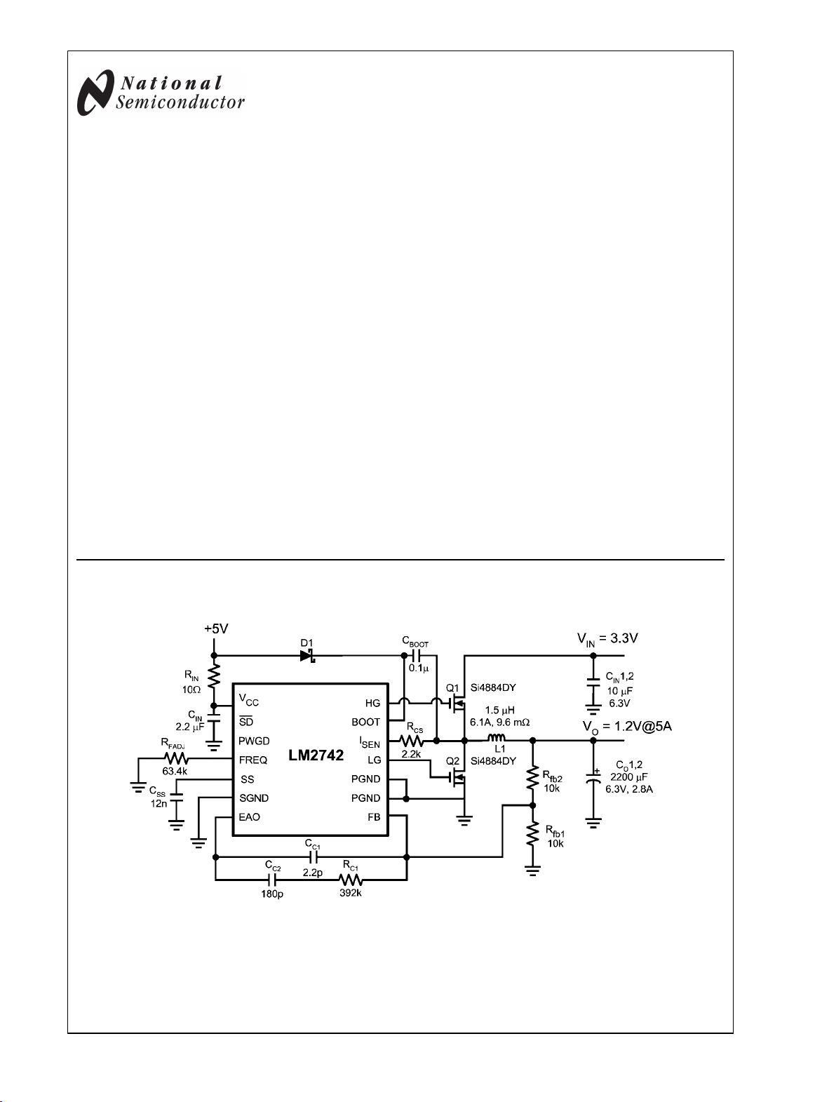
Typical Application
Features
Input power from 1V to 16V
■
Output voltage adjustable down to 0.6V
■
Power Good flag, adjustable soft-start and output enable
■
for easy power sequencing
Reference Accuracy: 1.5% (0°C - 125°C)
■
Current limit without sense resistor
■
Soft start
■
Switching frequency from 50 kHz to 2 MHz
■
40ns typical minimum on-time
■
TSSOP-14 package
■
Applications
POL power supply modules
■
Cable Modems
■
Set-Top Boxes/ Home Gateways
■
DDR Core Power
■
High-Efficiency Distributed Power
■
Local Regulation of Core Power
■
20087510
© 2007 National Semiconductor Corporation 200875 www.national.com
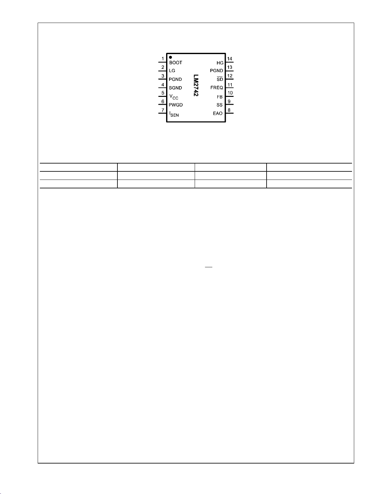
Connection Diagram
LM2742
14-Lead Plastic TSSOP
θJA = 155°C/W
20087511
Ordering Information
Order Number Package Type NSC Package Drawing Supplied As
LM2742MTC TSSOP-14 MTC14 94 Units, Raill
LM2742MTCX TSSOP-14 MTC14 2500 Units on Tape and Reel
Pin Descriptions
BOOT (Pin 1) - Supply rail for the N-channel MOSFET gate
drive. The voltage should be at least one gate threshold above
the regulator input voltage to properly turn on the high-side NFET.
LG (Pin 2) - Gate drive for the low-side N-channel MOSFET.
This signal is interlocked with HG to avoid shoot-through
problems.
PGND (Pins 3, 13) - Ground for FET drive circuitry. It should
be connected to system ground.
SGND (Pin 4) - Ground for signal level circuitry. It should be
connected to system ground.
VCC (Pin 5) - Supply rail for the controller.
PWGD (Pin 6) - Power Good. This is an open drain output.
The pin is pulled low when the chip is in UVP, OVP, or UVLO
mode. During normal operation, this pin is connected to V
or other voltage source through a pull-up resistor.
ISEN (Pin 7) - Current limit threshold setting. This sources a
fixed 50µA current. A resistor of appropriate value should be
connected between this pin and the drain of the low-side FET.
EAO (Pin 8) - Output of the error amplifier. The voltage level
on this pin is compared with an internally generated ramp
CC
signal to determine the duty cycle. This pin is necessary for
compensating the control loop.
SS (Pin 9) - Soft start pin. A capacitor connected between this
pin and ground sets the speed at which the output voltage
ramps up. Larger capacitor value results in slower output voltage ramp but also lower inrush current.
FB (Pin 10) - This is the inverting input of the error amplifier,
which is used for sensing the output voltage and compensating the control loop.
FREQ (Pin 11) - The switching frequency is set by connecting
a resistor between this pin and ground.
SD (Pin 12) - IC Logic Shutdown. When this pin is pulled low
the chip turns off both the high side and low side switches.
While this pin is low, the IC will not start up. An internal 20µA
pull-up connects this pin to VCC. For a device which turns on
the low side switch during shutdown, see the pin compatible
LM2737.
HG (Pin 14) - Gate drive for the high-side N-channel MOSFET. This signal is interlocked with LG to avoid shoot-through
problems.
www.national.com 2

Absolute Maximum Ratings (Note 1)
If Military/Aerospace specified devices are required,
please contact the National Semiconductor Sales Office/
Distributors for availability and specifications.
V
CC
BOOTV 21V
LG and HG to GND (Note 3) -2V to 21V
Junction Temperature 150°C
Storage Temperature −65°C to 150°C
7V
Lead Temperature
(soldering, 10sec) 260°C
Infrared or Convection (20sec) 235°C
ESD Rating 2 kV
Operating Ratings
Supply Voltage (VCC)
Junction Temperature Range −40°C to +125°C
Thermal Resistance (θJA)
4.5V to 5.5V
155°C/W
Soldering Information
Electrical Characteristics
VCC = 5V unless otherwise indicated. Typicals and limits appearing in plain type apply for TA=TJ=+25°C. Limits appearing in boldface
type apply over full Operating Temperature Range. Datasheet min/max specification limits are guaranteed by design, test, or
statistical analysis.
Symbol Parameter Conditions Min Typ Max Units
V
FB_ADJ
V
I
Q-V5
t
PWGD1
t
PWGD2
I
I
SS-ON
I
SS-OC
SD
ON
VCC = 4.5V, 0°C to +125°C
VCC = 5V, 0°C to +125°C
FB Pin Voltage
VCC = 5.5V, 0°C to +125°C
VCC = 4.5V, −40°C to +125°C
VCC = 5V, −40°C to +125°C
VCC = 5.5V, −40°C to +125°C
UVLO Thresholds Rising
Falling
SD = 5V, FB = 0.55V
Fsw = 600kHz
Operating VCC Current
SD = 5V, FB = 0.65V
Fsw = 600kHz 0.8 1.7
Shutdown VCC Current SD = 0V 0.15 0.4 0.7 mA
PWGD Pin Response Time FB Voltage Going Up 6 µs
PWGD Pin Response Time FB Voltage Going Down 6 µs
SD Pin Internal Pull-up Current 20 µA
SS Pin Source Current SS Voltage = 2.5V
0°C to +125°C
-40°C to +125°C
SS Pin Sink Current During Over
SS Voltage = 2.5V
Current
0.591 0.6 0.609
0.591 0.6 0.609
0.591 0.6 0.609
0.589 0.6 0.609
0.589 0.6 0.609
0.589 0.6 0.609
4.2
3.6
1 1.5 2
2.2
8
5
11
11
95
15
15
V
V
mA
µA
Symbol Parameter Conditions Min Typ Max Units
LM2742
GATE DRIVE
I
Q-BOOT
R
R
R
R
DS1
DS2
DS3
DS4
BOOT Pin Quiescent Current BOOT = 12V, EN = 0
0°C to +125°C
-40°C to +125°C
Top FET Driver Pull-Up ON
resistance
Top FET Driver Pull-Down ON
resistance
Bottom FET Driver Pull-Up ON
resistance
Bottom FET Driver Pull-Down ON
resistance
BOOT-SW = 5V@350mA
BOOT-SW = 5V@350mA
BOOT-SW = 5V@350mA
BOOT-SW = 5V@350mA
95
95
3
2
3
2
OSCILLATOR
50
300
500 600 700
490 600 700
1400
2000
90
88
f
OSC
PWM Frequency
D Max Duty Cycle f
t
on-min
Minimum on-time 40 ns
R
= 590kΩ
FADJ
R
= 88.7kΩ
FADJ
R
= 42.2kΩ, 0°C to +125°C
FADJ
R
= 42.2kΩ, -40°C to +125°C
FADJ
R
= 17.4kΩ
FADJ
R
= 11.3kΩ
FADJ
= 300kHz
PWM
f
= 600kHz
PWM
LOGIC INPUTS AND OUTPUTS
V
SD-IH
V
SD-IL
V
PWGD-TH-LO
V
PWGD-TH-HI
V
PWGD-HYS
SD Pin Logic High Trip Point 2.6 3.5 V
SD Pin Logic Low Trip Point 0°C to +125°C
-40°C to +125°C
1.3
1.25
1.6
1.6
PWGD Pin Trip Points FB Voltage Going Down
0°C to +125°C
-40°C to +125°C
0.413
0.410
0.430
0.430
0.446
0.446
PWGD Pin Trip Points FB Voltage Going Up
0°C to +125°C
-40°C to +125°C
PWGD Hysteresis FB Voltage Going Down FB Voltage
Going Up
0.691
0.688
35
0.710
0.710
110
0.734
0.734
160
215
%
µA
Ω
Ω
Ω
Ω
kHz
V
V
V
mV
Note 1: Absolute maximum ratings indicate limits beyond which damage to the device may occur. Operating ratings indicate conditions for which the device
operates correctly. Operating Ratings do not imply guaranteed performance limits.
Note 2: The human body model is a 100pF capacitor discharged through a 1.5k resistor into each pin.
Note 3: The LG and HG pin can have -2V to -0.5V applied for a maximum duty cycle of 10% with a maximum period of 1 second. There is no duty cycle or
maximum period limitation for a LG and HG pin voltage range of -0.5V to 21V.
www.national.com 4
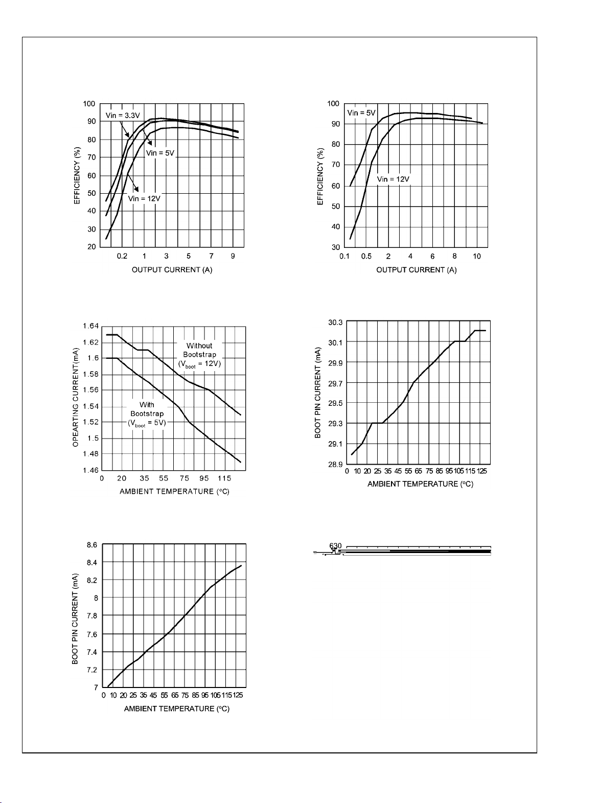
Typical Performance Characteristics
LM2742
Efficiency (VO = 1.5V)
FSW = 300kHz, TA = 25°C
20087512
VCC Operating Current vs Temperature
FSW = 600kHz, No-Load
Efficiency (VO = 3.3V)
FSW = 300kHz, TA = 25°C
20087513
Bootpin Current vs Temperature for BOOTV = 12V
FSW = 600kHz, Si4826DY FET, No-Load
20087514
Bootpin Current vs Temperature with 5V Bootstrap
FSW = 600kHz, Si4826DY FET, No-Load
20087516
20087515
PWM Frequency vs Temperature
for R
5 www.national.com
FADJ
= 43.2kΩ
20087517
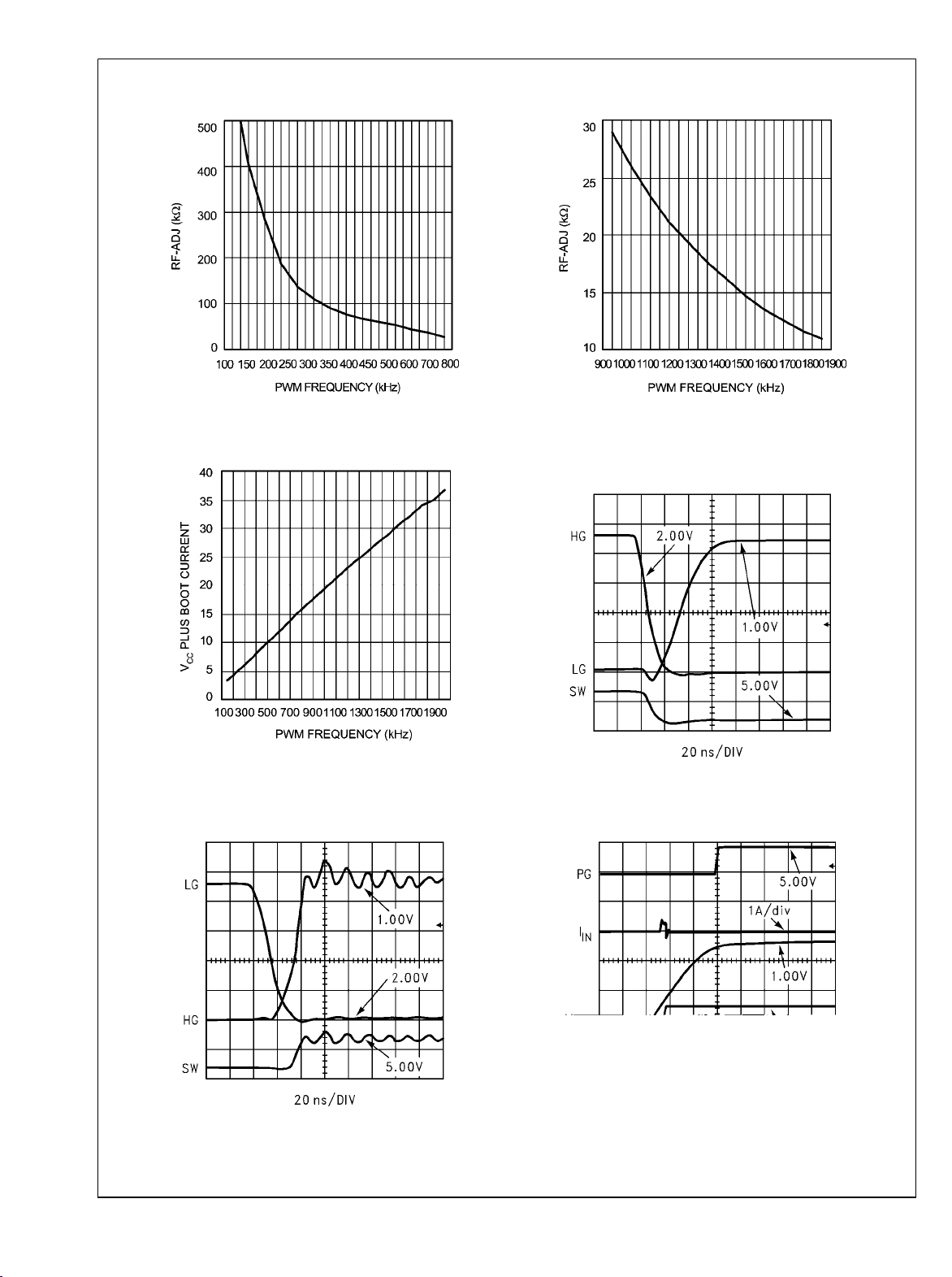
LM2742
R
vs PWM Frequency
FADJ
(in 100 to 800kHz range), TA = 25°C
R
vs PWM Frequency
FADJ
(in 900 to 2000kHz range), TA = 25°C
20087518
VCC Operating Current Plus Boot Current vs
PWM Frequency (Si4826DY FET, TA = 25°C)
20087520
Switch Waveforms (HG Rising)
VIN = 5V, VO = 1.8V
IO = 3A, FSW = 600kHz
20087519
Switch Waveforms (HG Falling)
VIN = 5V, VO = 1.8V
IO = 3A, CSS = 10nF
FSW = 600kHz
20087523
Start-Up (No-Load)
VIN = 10V, VO = 1.2V
CSS = 10nF, FSW = 300kHz
20087524
www.national.com 6
20087521
LM2742
Start-Up (Full-Load)
VIN = 10V, VO = 1.2V
IO = 10A, CSS = 10nF
FSW = 300kHz
Start Up (Full Load, 10x CSS)
VIN = 10V, VO = 1.2V
IO = 10A, CSS = 100nF
FSW = 300kHz
Start Up (No-Load, 10x CSS)
VIN = 10V, VO = 1.2V
CSS = 100nF, FSW = 300kHz
20087526
20087522
Start Up (Into 1.2V Pre-Bias)
VIN = 12V, VO = 2.5V
No Load, No Soft Start Capacitor
FSW = 300kHz
Start Up (Into 1.2V Pre-Bias)
VIN = 12V, VO = 2.5V
No Load, CSS = 10nF
FSW = 300kHz
20087525
20087549
20087548
Shutdown
VIN = 12V, VO = 1.2V
IO = 10A, CSS = 10nF
FSW = 300kHz
20087527
7 www.national.com
LM2742
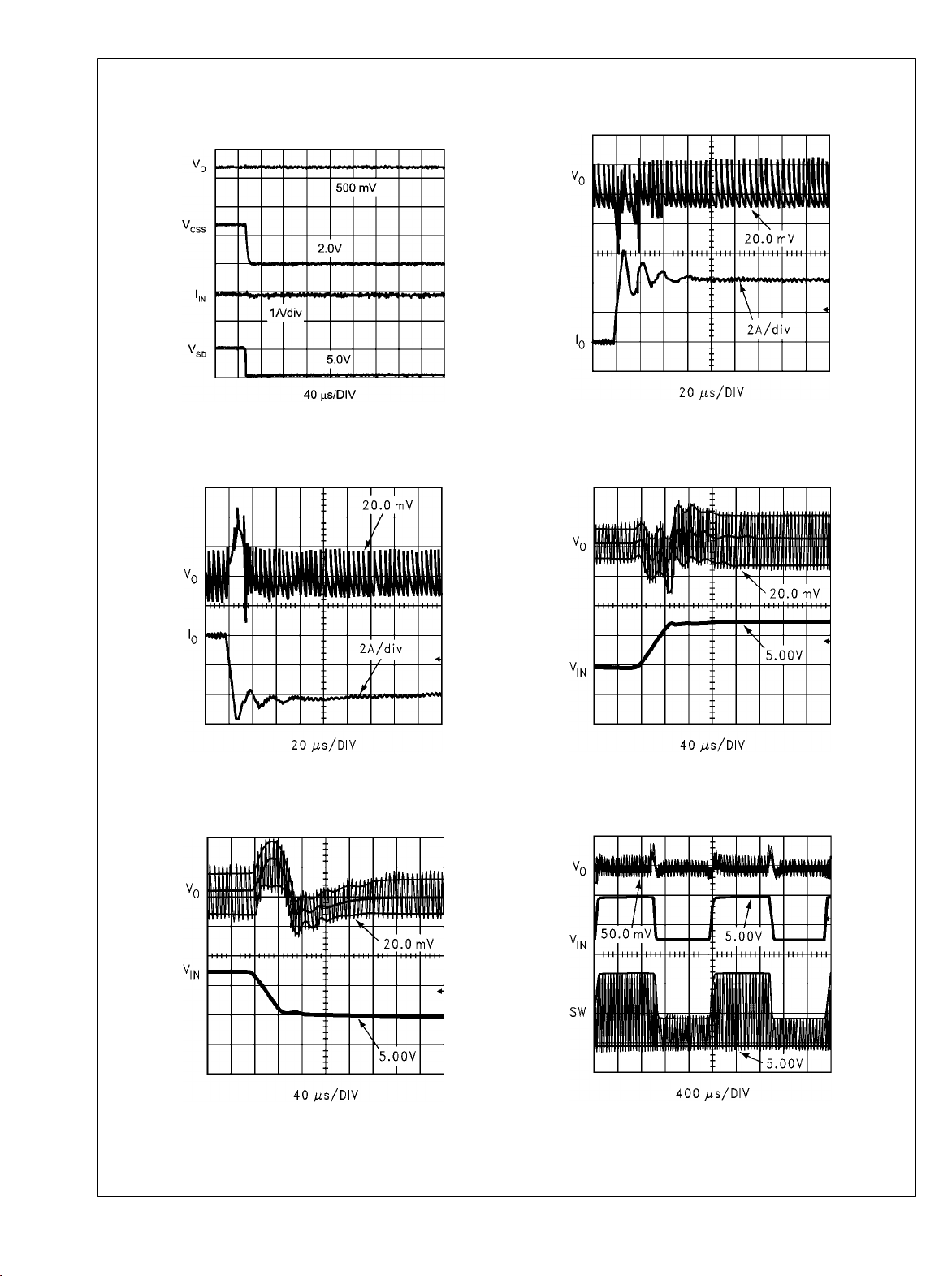
Shutdown (No Load)
VIN = 12V, VO = 1.2V
IO = 10A, CSS = 10nF
FSW = 300kHz
Load Transient Response (IO = 0 to 4A)
VIN = 12V, VO = 1.2V
FSW = 300kHz
20087533
Load Transient Response (IO = 4 to 0A)
VIN = 12V, VO = 1.2V
FSW = 300kHz
20087529
Line Transient Response (VIN =12V to 5V)
VO = 1.2V, IO = 5A
FSW = 300kHz
20087528
Line Transient Response (VIN =5V to 12V)
VO = 1.2V, IO = 5A
FSW = 300kHz
20087530
Line Transient Response
VO = 1.2V, IO = 5A
FSW = 300kHz
20087531
www.national.com 8
20087532
 Loading...