

July 2007
LM27313
1.6 MHz Boost Converter With 30V Internal FET Switch in
SOT-23
LM27313 1.6 MHz Boost Converter With 30V Internal FET Switch in SOT-23
General Description
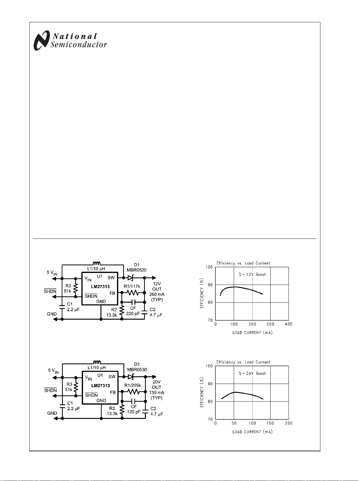
The LM27313 switching regulator is a current-mode boost
converter with a fixed operating frequency of 1.6 MHz.
The use of the SOT-23 package, made possible by the minimal losses of the 800 mA switch, and small inductors and
capacitors result in extremely high power density. The 30V
internal switch makes these solutions perfect for boosting to
voltages of 5V to 28V.
This part has a logic-level shutdown pin that can be used to
reduce quiescent current and extend battery life.
Protection is provided through cycle-by-cycle current limiting
and thermal shutdown. Internal compensation simplifies design and reduces component count.
Typical Application Circuits
Features
30V DMOS FET switch
■
1.6 MHz switching frequency
■
Low RDS(ON) DMOS FET
■
Switch current up to 800 mA
■
Wide input voltage range (2.7V–14V)
■
Low shutdown current (<1 µA)
■
5-Lead SOT-23 package
■
Uses tiny capacitors and inductors
■
Cycle-by-cycle current limiting
■
Internally compensated
■
Applications
White LED Current Source
■
PDA’s and Palm-Top Computers
■
Digital Cameras
■
Portable Phones, Games and Media Players
■
GPS Devices
■
20216824
20216857
20216801
20216858
© 2007 National Semiconductor Corporation 202168 www.national.com
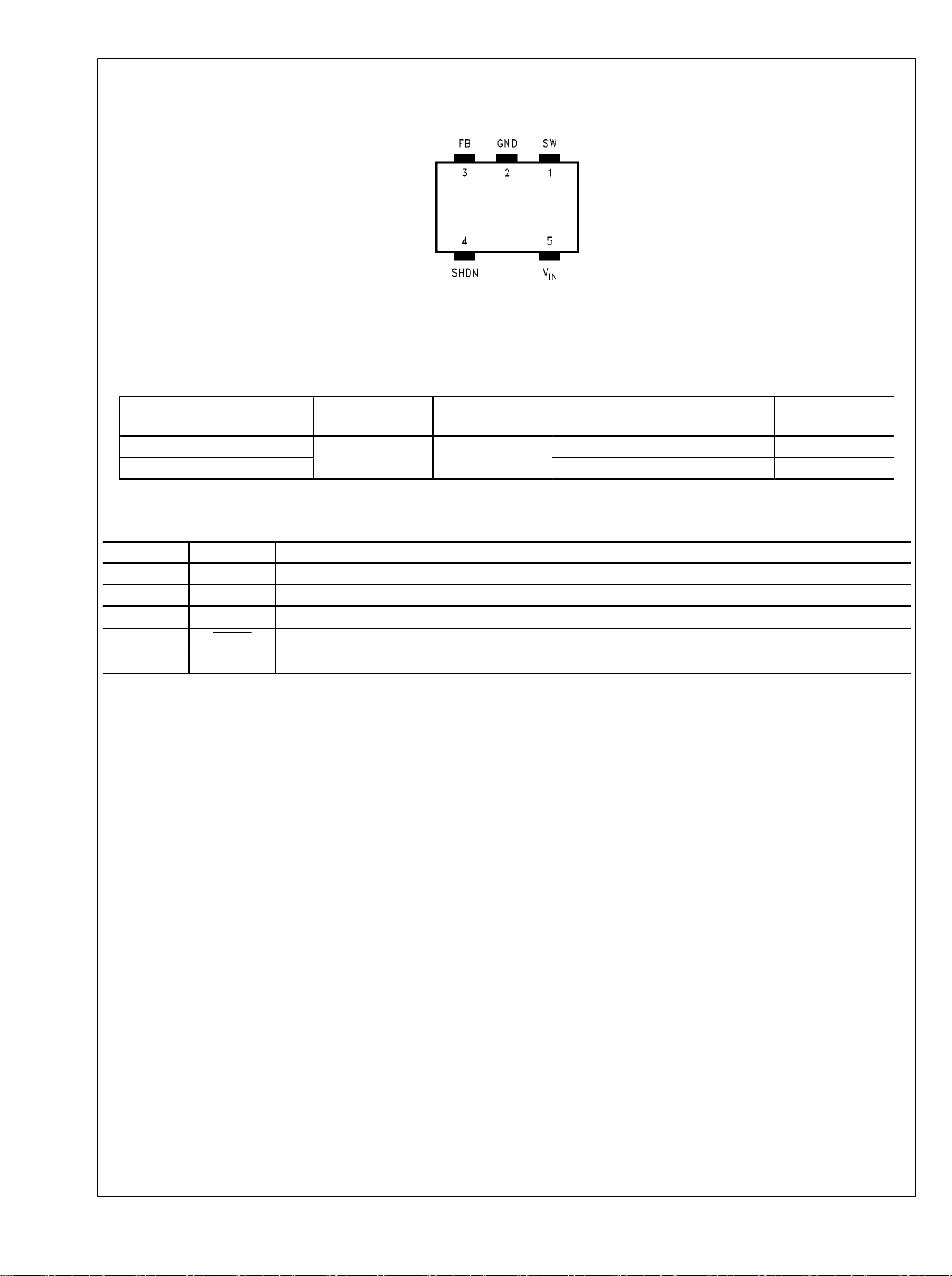
Connection Diagram
LM27313
Ordering Information
Order
Number
LM27313XMF
LM27313XMFX 3K Tape and Reel SRPB
Pin Descriptions
Pin Name Function
1 SW Drain of the internal FET switch.
2 GND Analog and power ground.
3 FB Feedback point that connects to external resistive divider to set V
4 SHDN Shutdown control input. Connect to VIN if this feature is not used.
5 V
IN
See NS Package Number MF05A
Package
Type
SOT23-5 MF05A
Analog and power input.
Top View
5-Lead SOT-23 Package
Package
Drawing
20216802
Supplied
As
1K Tape and Reel SRPB
.
OUT
Package
Marking
www.national.com 2

LM27313
Absolute Maximum Ratings (Note 1)
If Military/Aerospace specified devices are required,
please contact the National Semiconductor Sales Office/
Distributors for availability and specifications.
Storage Temperature Range −65°C to +150°C
Lead Temp. (Soldering, 5 sec.) 300°C
Power Dissipation (Note 2) Internally Limited
FB Pin Voltage −0.4V to +6V
SW Pin Voltage −0.4V to +30V
Input Supply Voltage −0.4V to +14.5V
Shutdown Input Voltage
(Survival) −0.4V to +14.5V
ESD Rating (Note 3)
Human Body Model
±2 kV
Operating Ratings
V
IN
V
SW(MAX)
V
SHDN
Junction Temperature, T
(Note 2)
θ
(SOT23-5)
J-A
J
2.7V to 14V
0V to V
-40°C to 125°C
265°C/W
Electrical Characteristics
Unless otherwise specified: VIN = 5V, V
limits in boldface type apply over the full operating temperature range (−40°C ≤ TJ ≤ +125°C). Minimum and Maximum limits are
guaranteed through test, design, or statistical correlation. Typical values represent the most likely parametric norm at TJ = 25°C,
and are provided for reference purposes only.
Symbol Parameter Conditions Min Typical Max Units
V
I
SW
R
DS(ON)
V
SHDN(TH)
I
SHDN
V
I
FB
I
ΔVFB/ΔV
f
SW
D
MAX
I
Note 1: Absolute Maximum Ratings indicate limits beyond which damage to the device may occur. Operating Ratings indicate conditions for which the device is
to be functional, but does not guarantee specific limits. For guaranteed specifications and conditions see the Electrical Characteristic table.
Note 2: The maximum power dissipation which can be safely dissipated for any application is a function of the maximum junction temperature, T
the junction-to-ambient thermal resistance for the SOT-23 package, θ
at any ambient temperature for designs using this device can be calculated using the formula:
Input Voltage 2.7 14 V
IN
Switch Current Limit (Note 4) 0.80 1.25 A
Switch ON Resistance
Shutdown Threshold
Shutdown Pin Bias Current
Feedback Pin Reference
FB
Voltage
Feedback Pin Bias Current
Quiescent Current
Q
FB Voltage Line Regulation
IN
Switching Frequency 1.15 1.6 1.90 MHz
Maximum Duty Cycle 80 88 %
Switch Leakage
L
= 5V, IL = 0 mA, and TJ = 25°C. Limits in standard typeface are for TJ = 25°C, and
SHDN
ISW = 100 mA
500 650
Device ON 1.5
Device OFF 0.50
V
= 0
SHDN
V
= 5V
SHDN
VIN = 3V
VFB = 1.23V
V
= 5V, Switching
SHDN
V
= 5V, Not Switching
SHDN
V
= 0
SHDN
2.7V ≤ VIN ≤ 14V
Not Switching, VSW = 5V
= 265°C/W, and the ambient temperature, TA. The maximum allowable power dissipation
J-A
0
0 2
1.205 1.230 1.255 V
60 nA
2.1 3.0 mA
400 500
0.024 1
0.02 %/V
1 µA
J(MAX)
mΩ
µA
µA
= 125°C,
30V
IN
V
If power dissipation exceeds the maximum specified above, the internal thermal protection circuitry will protect the device by reducing the output voltage as
required to maintain a safe junction temperature.
Note 3: The human body model is a 100 pF capacitor discharged through a 1.5 kΩ resistor into each pin. Test method is per JESD22-A114.
Note 4: Switch current limit is dependent on duty cycle. Limits shown are for duty cycles ≤ 50%. See Figure 3 in Application Information – MAXIMUM SWITCH
CURRENT section.
3 www.national.com
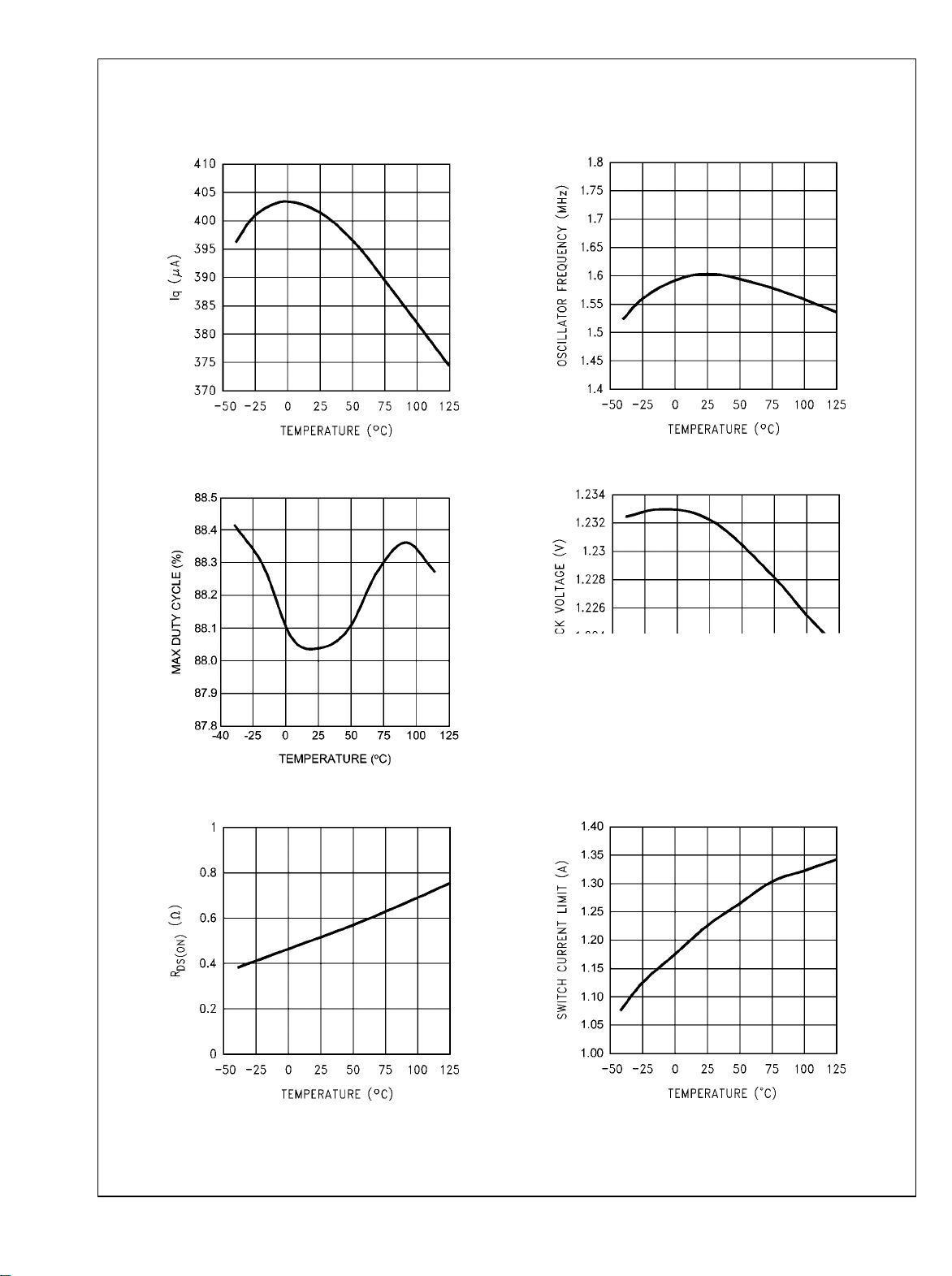
Typical Performance Characteristics Unless otherwise specified: V
TJ = 25°C.
LM27313
Iq VIN (Active) vs Temperature
Oscillator Frequency vs Temperature
= 5V, SHDN pin is tied to VIN,
IN
Max. Duty Cycle vs Temperature
RDS(ON) vs Temperature
20216810
20216855
20216808
Feedback Voltage vs Temperature
20216806
Current Limit vs Temperature
20216807
www.national.com 4
20216809
 Loading...