

National Semiconductor LM2703 Technical data
February 2002
LM2703
Micropower Step-up DC/DC Converter with 350mA Peak
Current Limit
LM2703 Micropower Step-up DC/DC Converter with 350mA Peak Current Limit
General Description
The LM2703 is a micropower step-up DC/DC in a small
5-lead SOT-23 package. A current limited, fixed off-time
control scheme conserves operating current resulting in high
efficiency over a wide range of load conditions. The 21V
switch allows for output voltages as high as 20V. The low
400ns off-time permits the use of tiny, low profile inductors
and capacitors to minimize footprint and cost in
space-conscious portable applications. The LM2703 is ideal
for LCD panels requiring low current and high efficiency as
well as white LED applications for cellular phone
back-lighting. The LM2703 can drive up to 4 white LEDs
from a single Li-Ion battery.
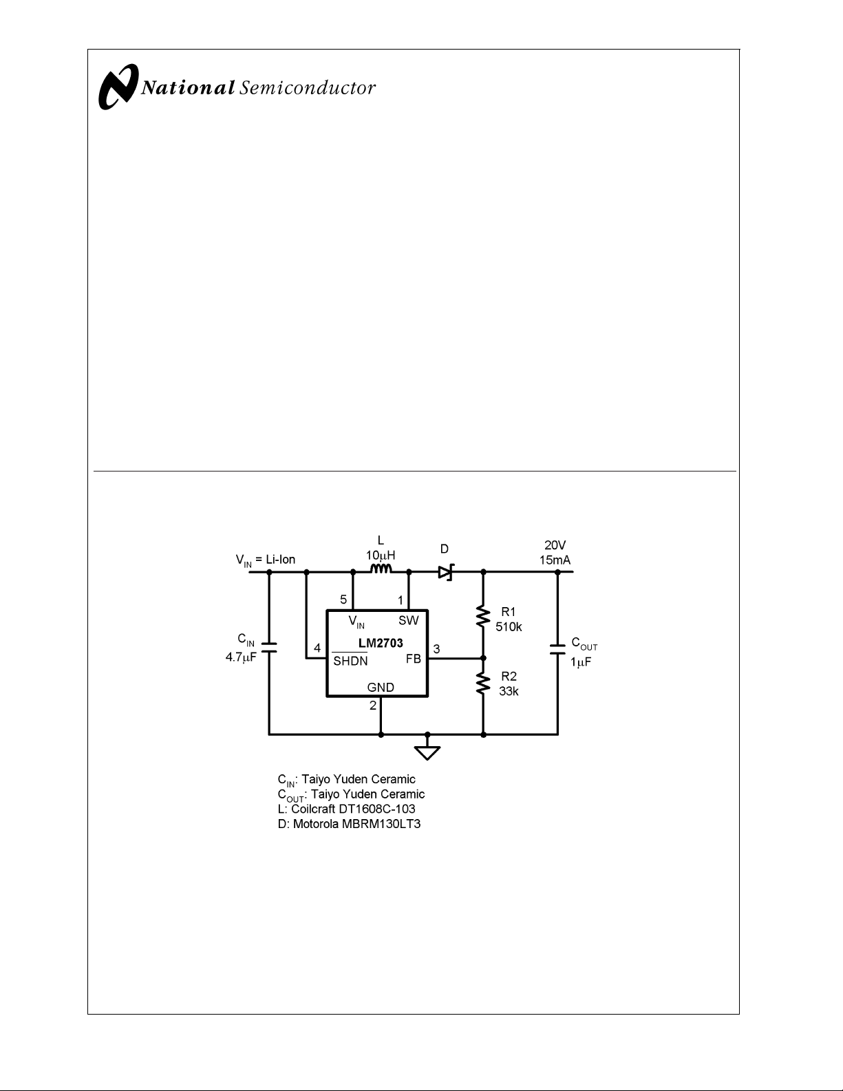
Typical Application Circuit
Features
n 350mA, 0.7Ω, internal switch
n Uses small surface mount components
n Adjustable output voltage up to 20V
n 2.2V to 7V input range
n Input undervoltage lockout
n 0.01µA shutdown current
n Small 5-Lead SOT-23 package
Applications
n LCD Bias Supplies
n White LED Back-Lighting
n Handheld Devices
n Digital Cameras
n Portable Applications
20030601
FIGURE 1. Typical 20V Application
© 2002 National Semiconductor Corporation DS200306 www.national.com
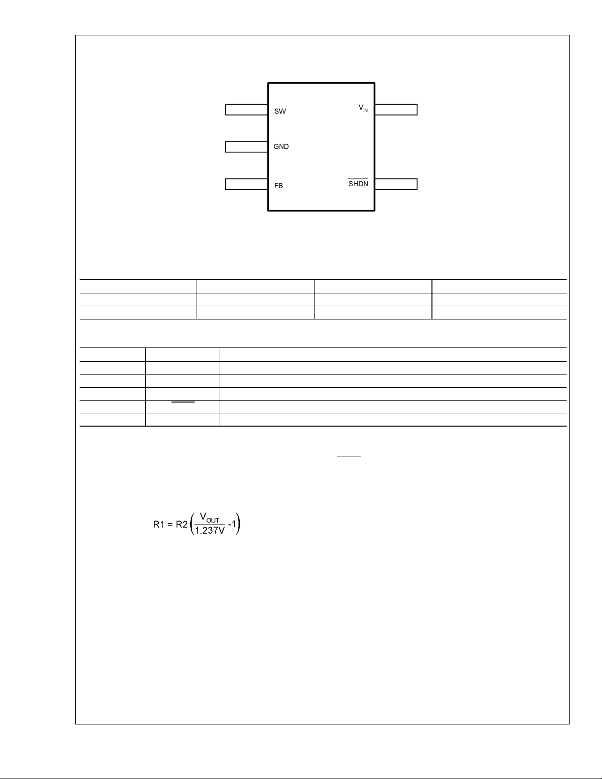
Connection Diagram
LM2703
Top View
SOT23-5
T
= 125˚C, θJA= 220˚C/W (Note 2)
Jmax
20030602
Ordering Information
Order Number Package Type NSC Package Drawing Supplied As
LM2703MF-ADJ SOT23-5 MA05B 1000 Units, Tape and Reel
LM2703MFX-ADJ SOT23-5 MA05B 3000 Units, Tape and Reel
Pin Description/Functions
Pin Name Function
1 SW Power Switch input.
2 GND Ground.
3 FB Output voltage feedback input.
4 SHDN
5V
SW(Pin 1): Switch Pin. This is the drain of the internal
NMOS power switch. Minimize the metal trace area connected to this pin to minimize EMI.
GND(Pin 2): Ground Pin. Tie directly to ground plane.
FB(Pin 3): FeedbackPin.Set the output voltage by selecting
values for R1 and R2 using:
IN
Shutdown control input, active low.
Analog and Power input.
Connect the ground of the feedback network to an AGND
plane which should be tied directly to the GND pin.
SHDN(Pin 4): Shutdown Pin. The shutdown pin is an active
low control. Tie this pin above 1.1V to enable the device. Tie
this pin below 0.3V to turn off the device.
V
IN
as close to the device as possible.
(Pin 5): Input Supply Pin. Bypass this pin with a capacitor
www.national.com 2
LM2703
Absolute Maximum Ratings (Note 1)
If Military/Aerospace specified devices are required,
please contact the National Semiconductor Sales Office/
Distributors for availability and specifications.
V
IN
7.5V
Infrared
(15 sec.) 220˚C
ESD Ratings (Note 3)
Human Body Model
Machine Model (Note 4)
200V
SW Voltage 21V
FB Voltage 2V
SHDN Voltage
Maximum Junction Temp. T
J
7.5V
150˚C
(Note 2)
Lead Temperature
(Soldering 10 sec.) 300˚C
Operating Conditions
Junction Temperature
(Note 5) −40˚C to +125˚C
Supply Voltage 2.2V to 7V
SW Voltage Max. 20.5V
Vapor Phase
(60 sec.) 215˚C
Electrical Characteristics
Specifications in standard type face are for TJ= 25˚C and those in boldface type apply over the full Operating Temperature
Range (T
Symbol Parameter Conditions
I
Q
V
FB
I
CL
I
B
V
IN
R
DSON
T
OFF
I
SD
I
L
UVP Input Undervoltage Lockout ON/OFF Threshold 1.8 V
V
FB
Hysteresis
SHDN
Threshold
θ
JA
Note 1: Absolute maximum ratings are limits beyond which damage to the device may occur. Operating Ratings are conditions for which the device is intended to
be functional, but device parameter specifications may not be guaranteed. For guaranteed specifications and test conditions, see the Electrical Characteristics.
Note 2: The maximum allowable power dissipation is a function of the maximum junction temperature, T
and the ambient temperature, T
temperature is calculated using: P
Note 3: The human body model is a 100 pF capacitor discharged through a 1.5 kΩ resistor into each pin. The machine model is a 200 pF capacitor discharged
directly into each pin.
Note 4: ESD susceptibility using the machine model is 150V for SW pin.
Note 5: All limits guaranteed at room temperature (standard typeface) and at temperature extremes (bold typeface). All room temperature limits are 100%
production tested or guaranteed through statistical analysis. All limits at temperature extremes are guaranteed via correlation using standard Statistical Quality
Control (SQC) methods. All limits are used to calculate Average Outgoing Quality Level (AOQL).
Note 6: Typical numbers are at 25˚C and represent the most likely norm.
Note 7: Feedback current flows into the pin.
= −40˚C to +125˚C). Unless otherwise specified. VIN=2.2V.
J
Min
(Note 5)
Typ
(Note 6)
Max
(Note 5)
Device Disabled FB = 1.3V 40 70
Shutdown SHDN = 0V
0.01 2.5
FeedbackTrip Point 1.189 1.237 1.269 V
Switch Current Limit 275
260
350 400
400
FB Pin Bias Current FB = 1.23V (Note 7) 30 120 nA
Input Voltage Range 2.2 7.0 V
Switch R
DSON
0.7 1.6 Ω
Switch Off Time 400 ns
SHDN Pin Current SHDN = VIN,TJ= 25˚C 080
= 125˚C 15
IN,TJ
SHDN = GND
0
Switch Leakage Current VSW= 20V 0.05 5 µA
Feedback Hysteresis 8 mV
SHDN low
SHDN High
1.1 0.7
0.7 0.3
Thermal Resistance 220 ˚C/W
(MAX), the junction-to-ambient thermal resistance, θJA,
. See the Electrical Characteristics table for the thermal resistance. The maximum allowable power dissipation at any ambient
A
(MAX) = (T
D
J(MAX)−TA
)/θJA. Exceeding the maximum allowable power dissipation will cause excessive die temperature.
J
Units
mA
2kV
µADevice Enabled FB = 1.2V 235 300
nASHDN = V
V
www.national.com3
 Loading...