

National Semiconductor LM2670 Technical data
February 29, 2008
LM2670
SIMPLE SWITCHER® High Efficiency 3A Step-Down
Voltage Regulator with Sync
LM2670 SIMPLE SWITCHER High Efficiency 3A Step-Down Voltage Regulator with Sync
General Description
The LM2670 series of regulators are monolithic integrated
circuits which provide all of the active functions for a stepdown (buck) switching regulator capable of driving up to 3A
loads with excellent line and load regulation characteristics.
High efficiency (>90%) is obtained through the use of a low
ON-resistance DMOS power switch. The series consists of
fixed output voltages of 3.3V, 5V and 12V and an adjustable
output version.
The SIMPLE SWITCHER concept provides for a complete
design using a minimum number of external components. The
switching clock frequency can be provided by an internal fixed
frequency oscillator (260KHz) or from an externally provided
clock in the range of 280KHz to 400Khz which allows the use
of physically smaller sized components. A family of standard
inductors for use with the LM2670 are available from several
manufacturers to greatly simplify the design process. The external Sync clock provides direct and precise control of the
output ripple frequency for consistent filtering or frequency
spectrum positioning.
The LM2670 series also has built in thermal shutdown, current limiting and an ON/OFF control input that can power
down the regulator to a low 50μA quiescent current standby
condition. The output voltage is guaranteed to a ±2% tolerance.
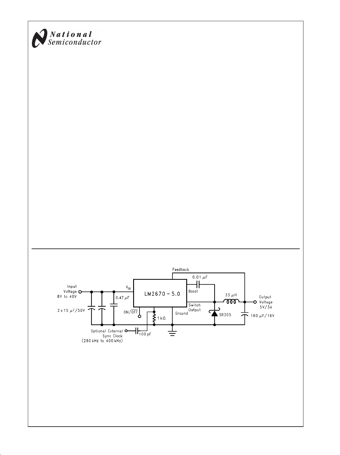
Typical Application
Features
Efficiency up to 94%
■
Simple and easy to design with (using off-the-shelf
■
external components)
150 mΩ DMOS output switch
■
3.3V, 5V and 12V fixed output and adjustable (1.2V to
■
37V ) versions
50μA standby current when switched OFF
■
±2%maximum output tolerance over full line and load
■
conditions
Wide input voltage range: 8V to 40V
■
External Sync clock capability (280KHz to 400KHz)
■
260 KHz fixed frequency internal oscillator
■
−40 to +125°C operating junction temperature range
■
Applications
Simple to design, high efficiency (>90%) step-down
■
switching regulators
Efficient system pre-regulator for linear voltage regulators
■
Battery chargers
■
Communications and radio equipment regulator with
■
synchronized clock frequency
10094203
SIMPLE SWITCHER® is a registered trademark of National Semiconductor Corporation
© 2008 National Semiconductor Corporation 100942 www.national.com
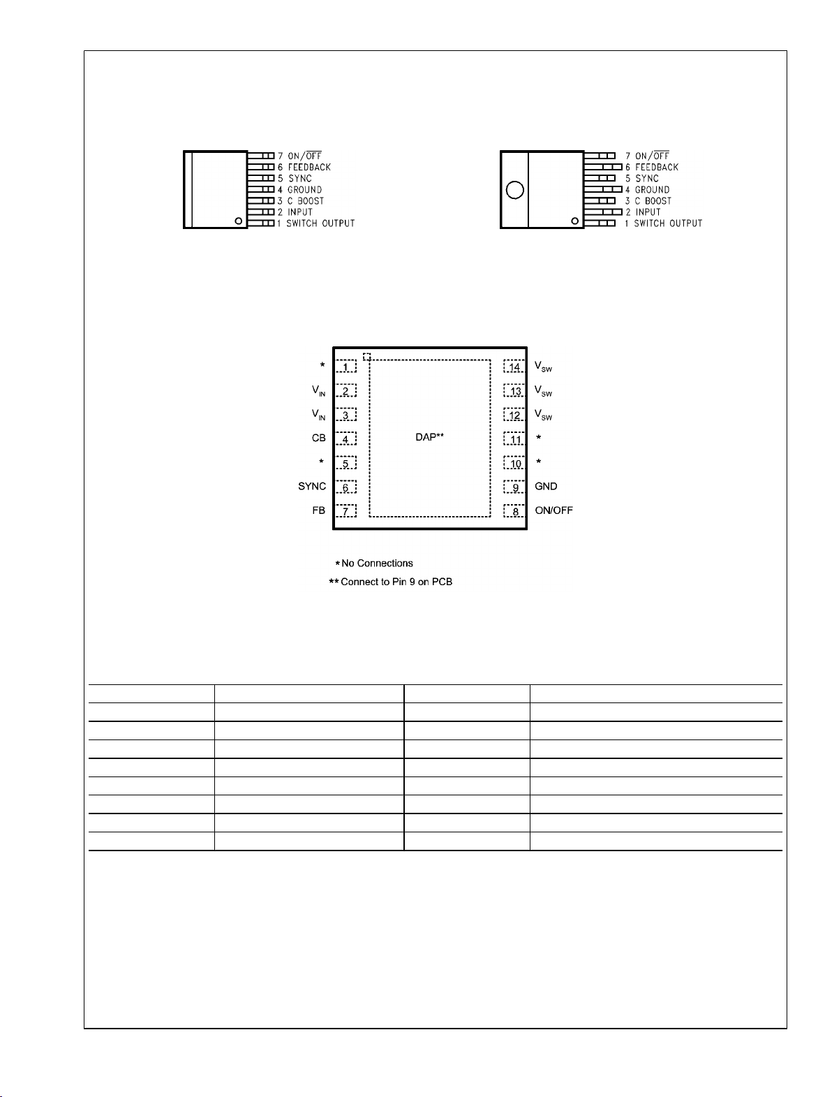
Connection Diagrams and Ordering Information
LM2670
TO-263 Package
Top View
Order Number
LM2670S-3.3, LM2670S-5.0,
LM2670S-12 or LM2670S-ADJ
See NSC Package Number TS7B
10094201
Top View
TO-220 Package
Top View
Order Number
LM2670T-3.3, LM2670T-5.0,
LM2670T-12 or LM2670T-ADJ
See NSC Package Number TA07B
10094202
See NS package Number SRC14A
LLP-14
10094241
Ordering Information for LLP Package
Output Voltage Order Information Package Marking Supplied As
12 LM2670SD-12 S0002LB 250 Units on Tape and Reel
12 LM2670SDX-12 S0002LB 2500 Units on Tape and Reel
3.3 LM2670SD-3.3 S0002NB 250 Units on Tape and Reel
3.3 LM2670SDX-3.3 S0002NB 2500 Units on Tape and Reel
5.0 LM2670SD-5.0 S0002PB 250 Units on Tape and Reel
5.0 LM2670SDX-5.0 S0002PB 2500 Units on Tape and Reel
ADJ LM2670SD-ADJ S0002RB 250 Units on Tape and Reel
ADJ LM2670SDX-ADJ S0002RB 2500 Units on Tape and Reel
www.national.com 2
LM2670
Absolute Maximum Ratings (Note 1)
If Military/Aerospace specified devices are required,
please contact the National Semiconductor Sales Office/
Distributors for availability and specifications.
Input Supply Voltage 45V
ON/OFF Pin Voltage −0.1V to 6V
Switch Voltage to Ground (Note 12) −1V to V
Boost Pin Voltage VSW + 8V
Feedback Pin Voltage −0.3V to 14V
Power Dissipation Internally Limited
IN
ESD (Note 2) 2 kV
Storage Temperature Range −65°C to 150°C
Soldering Temperature
Wave 4 sec, 260°C
Infrared 10 sec, 240°C
Vapor Phase 75 sec, 219°C
Operating Ratings
Supply Voltage 8V to 40V
Junction Temperature Range (TJ)
−40°C to 125°C
Electrical Characteristics Limits appearing in bold type face apply over the entire junction temperature range
of operation, −40°C to 125°C. Specifications appearing in normal type apply for TA = TJ = 25°C. Sync pin open circuited.
LM2670-3.3
Symbol Parameter Conditions Typical Min Max Units
V
OUT
η
Output Voltage
Efficiency VIN = 12V, I
VIN = 8V to 40V, 100mA ≤ I
LOAD
(Note 3) (Note 4) (Note 4)
≤ 3A
OUT
= 3A 86 %
3.3 3.234/3.201 3.366/3.399 V
LM2670-5.0
Symbol Parameter Conditions Typical Min Max Units
V
OUT
η
Output Voltage
Efficiency VIN = 12V, I
VIN = 8V to 40V, 100mA ≤ I
LOAD
(Note 3) (Note 4) (Note 4)
≤ 3A
OUT
= 3A 88 %
5.0 4.900/4.850 5.100/5.150 V
LM2670-12
Symbol Parameter Conditions Typical Min Max Units
V
OUT
η
Output Voltage
Efficiency VIN = 24V, I
VIN = 15V to 40V, 100mA ≤ I
LOAD
(Note 3) (Note 4) (Note 4)
≤ 3A
OUT
= 3A 94 %
12 11.76/11.64 12.24/12.36 V
LM2670-ADJ
Symbol Parameter Conditions Typ Min Max Units
V
FB
η
Feedback Voltage
Efficiency VIN = 12V, I
VIN = 8V to 40V, 100mA ≤ I
V
Programmed for 5V
OUT
LOAD
(Note 3) (Note 4) (Note 4)
≤ 3A
OUT
= 3A 88 %
1.21 1.186/1.174 1.234/1.246 V
3 www.national.com
All Output Voltage Versions Electrical Characteristics
LM2670
Limits appearing in bold type face apply over the entire junction temperature range of operation, −40°C to 125°C.
Specifications appearing in normal type apply for TA = TJ = 25°C. Unless otherwise specified VIN=12V for the 3.3V, 5V and Adjustable versions and VIN=24V for the 12V version, Sync pin open circuited..
Symbol Parameter Conditions Typ Min Max Units
DEVICE PARAMETERS
I
Q
I
STBY
I
CL
I
L
R
DS(ON)
f
O
D Duty Cycle Maximum Duty Cycle 91 %
I
BIAS
V
ON/OFF
I
ON/OFF
F
SYNC
V
SYNC
θ
JA
(Note 5)
θ
JA
(Note 6)
θ
JC
θ
JA
(Note 7)
θ
JA
(Note 8)
θ
JA
(Note 9)
θ
JC
θ
JA
(Note 10)
θ
JA
Quiescent Current V
FEEDBACK
= 8V
4.2
6 mA
For 3.3V, 5.0V, and ADJ Versions
V
FEEDBACK
= 15V
For 12V Versions
Standby Quiescent
Current
Current Limit
Output Leakage
Current
Switch OnResistance
Oscillator
Frequency
ON/OFF Pin = 0V
VIN = 40V, ON/OFF Pin = 0V
V
= 0V
SWITCH
V
= −1V
SWITCH
I
= 3A
SWITCH
Measured at Switch Pin
50 100/150
4.5 3.8/3.6 5.25/5.4 A
16
0.15
200
15
0.17/0.29
260 225 280 kHz
Minimum Duty Cycle 0 %
Feedback Bias
Current
ON/OFF
Threshold Voltage
ON/OFF Input
Current
Synchronization
Frequency
SYNC Threshold
Voltage
Thermal
V
FEEDBACK
ADJ Version Only
ON/OFF Input = 0V
V
SYNC
= 1.3V
(Pin 5)=3.5V, 50% Duty Cycle
85
nA
1.4 0.8 2.0 V
20
400
1.4
45
T Package, Junction to Ambient 65
Resistance
T Package, Junction to Ambient 45
T Package, Junction to Case 2
S Package, Junction to Ambient 56
S Package, Junction to Ambient 35
S Package, Junction to Ambient 26
S Package, Junction to Case 2 ++
SD Package, Junction to Ambient 55
SD Package, Junction to Ambient 29
(Note 11)
μA
μA
mA
Ω
μA
KHz
V
°C/W
°C/W
Note 1: Absolute Maximum Ratings are limits beyond which damage to the device may occur. Operating Ratings indicate conditions under which of the device
is guaranteed. Operating Ratings do not imply guaranteed performance limits. For guaranteed performance limits and associated test condition, see the electrical
Characteristics tables.
www.national.com 4

Note 2: ESD was applied using the human-body model, a 100pF capacitor discharged through a 1.5 kΩ resistor into each pin.
Note 3: Typical values are determined with TA = TJ = 25°C and represent the most likely norm.
Note 4: All limits are guaranteed at room temperature (standard type face) and at temperature extremes (bold type face). All room temperature limits are 100%
tested during production with TA = TJ = 25°C. All limits at temperature extremes are guaranteed via correlation using standard standard Quality Control (SQC)
methods. All limits are used to calculate Average Outgoing Quality Level (AOQL).
Note 5: Junction to ambient thermal resistance (no external heat sink) for the 7 lead TO-220 package mounted vertically, with ½ inch leads in a socket, or on a
PC board with minimum copper area.
Note 6: Junction to ambient thermal resistance (no external heat sink) for the 7 lead TO-220 package mounted vertically, with ½ inch leads soldered to a PC
board containing approximately 4 square inches of (1 oz.) copper area surrounding the leads.
Note 7: Junction to ambient thermal resistance for the 7 lead TO-263 mounted horizontally against a PC board area of 0.136 square inches (the same size as
the TO-263 package) of 1 oz. (0.0014 in. thick) copper.
Note 8: Junction to ambient thermal resistance for the 7 lead TO-263 mounted horizontally against a PC board area of 0.4896 square inches (3.6 times the area
of the TO-263 package) of 1 oz. (0.0014 in. thick) copper.
Note 9: Junction to ambient thermal resistance for the 7 lead TO-263 mounted horizontally against a PC board copper area of 1.0064 square inches (7.4 times
the area of the TO-263 package) of 1 oz. (0.0014 in. thick) copper. Additional copper area will reduce thermal resistance further. See the thermal model in Switchers
Made Simple® software.
Note 10: Junction to ambient thermal resistance for the 14-lead LLP mounted on a PC board copper area equal to the die attach paddle.
Note 11: Junction to ambient thermal resistance for the 14-lead LLP mounted on a PC board copper area using 12 vias to a second layer of copper equal to die
attach paddle. Additional copper area will reduce thermal resistance further. For layout recommendations, refer to Application Note AN-1187.
Note 12: The absolute maximum specification of the 'Switch Voltage to Ground' applies to DC voltage. An extended negative voltage limit of -8V applies to a
pulse of up to 20 ns, -6V of 60 ns and -3V of up to 100 ns.
LM2670
5 www.national.com

Typical Performance Characteristics
LM2670
Normalized
Output Voltage
Efficiency vs Input Voltage
10094209
Line Regulation
Efficiency vs I
10094210
LOAD
Switch Current Limit
10094211
10094204
10094212
Operating Quiescent Current
10094205
www.national.com 6
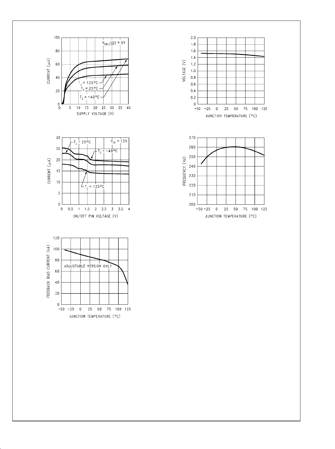
LM2670
Standby Quiescent Current
10094240
ON/OFF Pin Current (Sourcing)
ON/OFF Threshold Voltage
10094213
Switching Frequency
Feedback Pin Bias Current
10094214
10094216
10094215
7 www.national.com
Typical Performance Characteristics
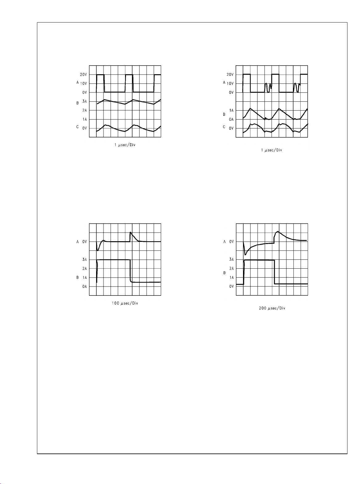
LM2670
Continuous Mode Switching Waveforms
VIN = 20V, V
L = 33 μH, C
A: VSW Pin Voltage, 10 V/div.
B: Inductor Current, 1 A/div
C: Output Ripple Voltage, 20 mV/div AC-Coupled
= 200 μF, C
OUT
Horizontal Time Base: 1 μs/div
Load Transient Response for Continuous Mode
VIN = 20V, V
L = 33 μH, C
= 200 μF, C
OUT
OUT
= 5V, I
OUT
= 3A
LOAD
ESR = 26 mΩ
OUT
10094217
= 5V
ESR = 26 mΩ
OUT
Discontinuous Mode Switching Waveforms
VIN = 20V, V
L = 10 μH, C
A: VSW Pin Voltage, 10 V/div.
B: Inductor Current, 1 A/div
C: Output Ripple Voltage, 20 mV/div AC-Coupled
OUT
= 400 μF, C
OUT
= 5V, I
= 500 mA
LOAD
ESR = 13 mΩ
OUT
10094218
Horizontal Time Base: 1 μs//iv
Load Transient Response for Discontinuous Mode
L = 10 μH, C
VIN = 20V, V
= 400 μF, C
OUT
OUT
= 5V,
OUT
ESR = 13 mΩ
A: Output Voltage, 100 mV//div, AC-Coupled.
10094219
B: Load Current: 500 mA to 3A Load Pulse
Horizontal Time Base: 100 μs/div
www.national.com 8
A: Output Voltage, 100 mV/div, AC-Coupled.
10094220
B: Load Current: 200 mA to 3A Load Pulse
Horizontal Time Base: 200 μs/div
 Loading...