

LM2660/LM2661
Switched Capacitor Voltage Converter
LM2660/LM2661 Switched Capacitor Voltage Converter
September 1999
General Description
The LM2660/LM2661 CMOS charge-pump voltage converter inverts a positive voltage in the range of 1.5V to 5.5V
to thecorresponding negative voltage. The LM2660/LM2661
uses two low cost capacitors to provide 100 mA of output
current without the cost, size, and EMI related to inductor
based converters. With an operating current of only 120 µA
and operating efficiency greater than 90%at most loads, the
LM2660/LM2661 provides ideal performance for battery
powered systems. The LM2660/LM2661 may also be used
as a positive voltage doubler.
The oscillator frequency can be lowered by adding an external capacitor to the OSC pin.Also, the OSC pin may be used
to drive the LM2660/LM2661 with an external clock. For
LM2660, a frequency control (FC) pin selects the oscillator
frequency of 10 kHz or 80 kHz. For LM2661, an external
shutdown (SD) pin replaces the FC pin. The SD pin can be
used to disable the device and reduce the quiescent current
to 0.5 µA. The oscillator frequency for the LM2661 is 80 kHz.
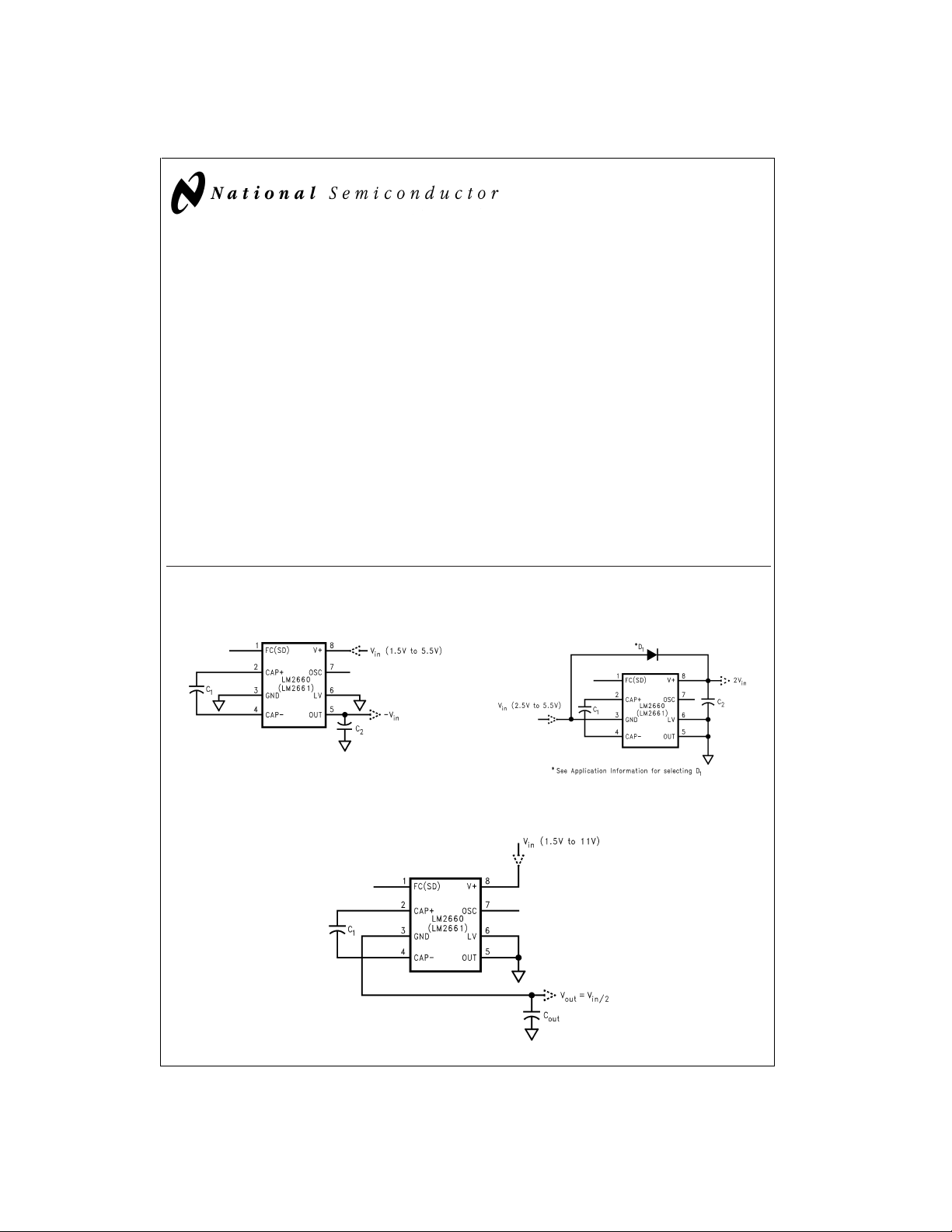
Basic Application Circuits
Voltage Inverter
DS012911-3
Features
n Inverts or doubles input supply voltage
n Narrow SO-8 and Mini SO-8 Package
n 6.5Ω typical output resistance
n 88%typical conversion efficiency at 100 mA
n (LM2660) selectable oscillator frequency: 10 kHz/80 kHz
n (LM2661) low current shutdown mode
Applications
n Laptop computers
n Cellular phones
n Medical instruments
n Operational amplifier power supplies
n Interface power supplies
n Handheld instruments
Positive Voltage Doubler
DS012911-4
Splitting VINin Half
DS012911-26
© 1999 National Semiconductor Corporation DS012911 www.national.com
Absolute Maximum Ratings (Note 1)
If Military/Aerospace specified devices are required,
please contact the National Semiconductor Sales Office/
Distributors for availability and specifications.
Supply Voltage (V+ to GND, or GND to OUT) 6V
LM2660/LM2661
LV (OUT − 0.3V) to (GND + 3V)
FC, OSC The least negative of (OUT − 0.3V)
V+ and OUT Continuous Output Current 120 mA
Output Short-Circuit Duration to GND (Note 2) 1 sec.
or (V+ − 6V) to (V+ + 0.3V)
Power Dissipation
=
25˚C) (Note 3) 735 mW 500 mW
(T
A
Max (Note 3) 150˚C 150˚C
T
J
(Note 3) 170˚C/W 250˚C/W
θ
JA
Operating Junction
Temperature
Range −40˚C to +85˚C
Storage Temperature Range −65˚C to +150˚C
Lead Temperature 300˚C
Package
MMM
(Soldering, 10 seconds)
ESD Rating 2 kV
Electrical Characteristics
Limits in standard typeface are for T
less otherwise specified: V+=5V, FC=Open, C
Symbol Parameter Condition Min Typ Max Units
V+ Supply Voltage R
I
Q
I
SD
Supply Current No Load FC=Open (LM2660) 0.12 0.5
Shutdown Supply Current
(LM2661)
V
SD
Shutdown Pin Input Voltage Shutdown Mode 2.0 (Note 5)
(LM2661) Normal Operation 0.3
I
L
R
OUT
f
OSC
f
SW
I
OSC
P
EFF
V
OEFF
Note 1: Absolute maximum ratings indicate limits beyond which damage to the device may occur. Electrical specifications do not apply when operating the device
beyond its rated operating conditions.
Note 2: OUT may be shorted to GND for one second without damage. However, shorting OUT to V+ may damage the device and should be avoided. Also, for temperatures above 85˚C, OUT must not be shorted to GND or V+, or device may be damaged.
Note 3: The maximum allowable power dissipation is calculated by using P
ambient temperature, and θ
Note 4: In the test circuit, capacitors C
age and efficiency.
Note 5: In doubling mode, when V
Note 6: Specified output resistance includes internal switch resistance and capacitor ESR.
Note 7: For LM2661, the oscillator frequency is 80 kHz.
Note 8: The output switches operate at one half of the oscillator frequency, f
Output Current TA≤ +85˚C, OUT ≤ −4V 100
Output Resistance (Note 6) I
Oscillator Frequency (Note 7) OSC=Open FC=Open 5 10
Switching Frequency (Note 8) OSC=Open FC=Open 2.5 5
OSC Input Current FC=Open
Power Efficiency RL(1k) between V+and OUT 96 98
Voltage Conversion Efficiency No Load 99 99.96
is the junction-to-ambient thermal resistance of the specified package.
JA
out
=
25˚C, and limits in boldface type apply over the full operating temperature range. Un-
J
=
=
C
150 µF. (Note 4)
1
2
=
1k Inverter, LV=Open 3.5 5.5
L
Inverter, LV=GND 1.5 5.5 V
Doubler, LV=OUT 2.5 5.5
SD=Ground (LM2661)
1 3
0.5 2 µA
>
+85˚C, OUT ≤ −3.8V 100
T
A
=
100 mA T
L
≤ +85˚C 6.5 10
A
>
+85˚C 12
T
A
FC=V+ 40 80
FC=V+ 20 40
±
2
±
FC=V+
R
(500) between GND and OUT 92 96
L
=
I
100 mA to GND 88
L
=
DMax
and C2are 0.2Ω maximum ESR capacitors. Capacitors with higher ESR will increase output resistance, reduce output volt-
1
>
5V, minimum input high for shutdown equals V
=
OSC
(T
JMax−TA
out
2f
SW
−3V.
.
)/θJA, where T
is the maximum junction temperature, TAis the
JMax
16
mALV=Open FC=V+ (LM2660) or
V
mA
Ω
kHz
kHz
µA
%
%
www.national.com 2
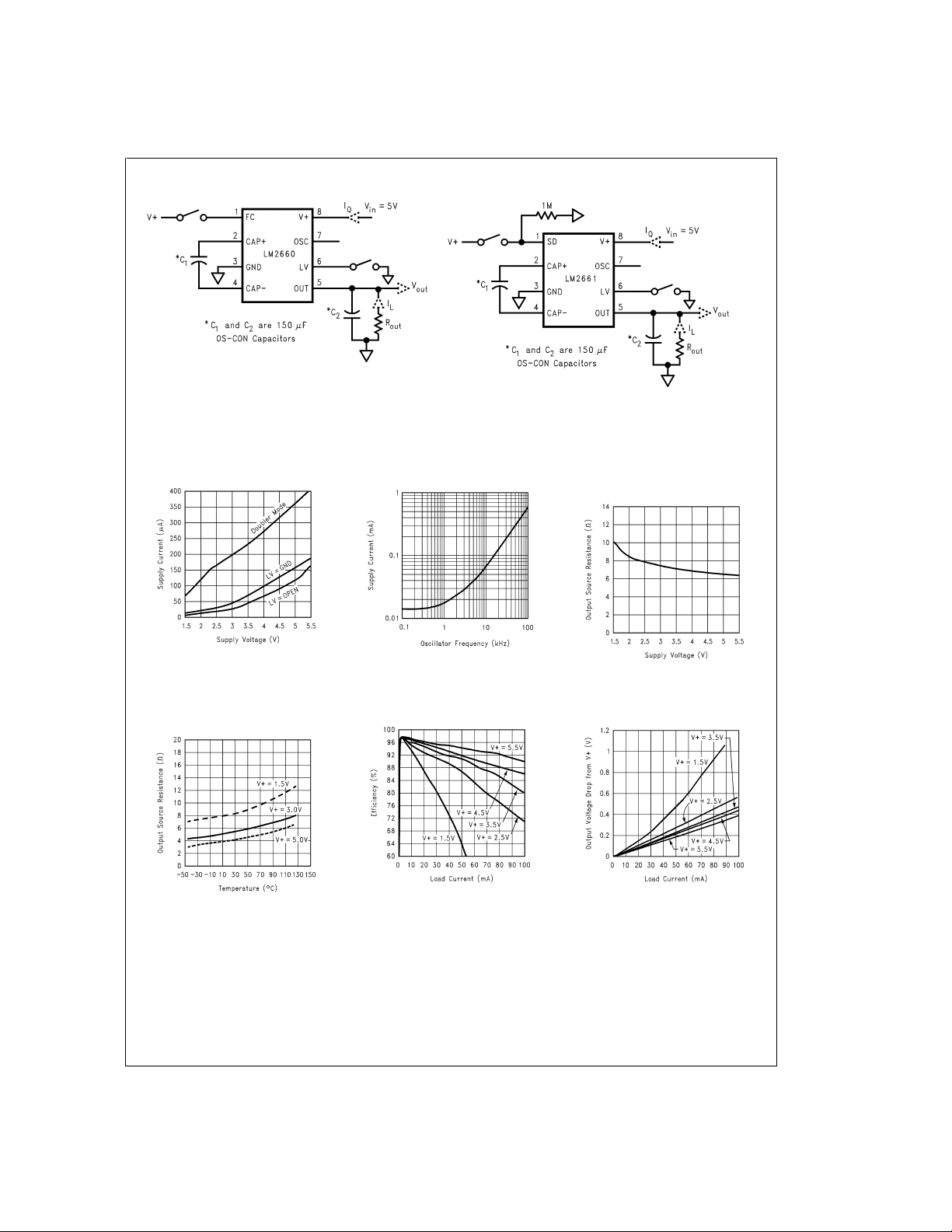
Test Circuits
DS012911-5
FIGURE 1. LM2660 and LM2661 Test Circuits
Typical Performance Characteristics
(Circuit of
Figure 1
LM2660/LM2661
DS012911-6
)
Supply Current vs
Supply Voltage
Output Source
Resistance vs
Temperature
DS012911-7
DS012911-10
Supply Current vs
Oscillator Frequency
Efficiency vs Load
Current
DS012911-8
DS012911-11
Output Source
Resistance vs Supply
Voltage
DS012911-9
Output Voltage Drop
vs Load Current
DS012911-12
www.national.com3
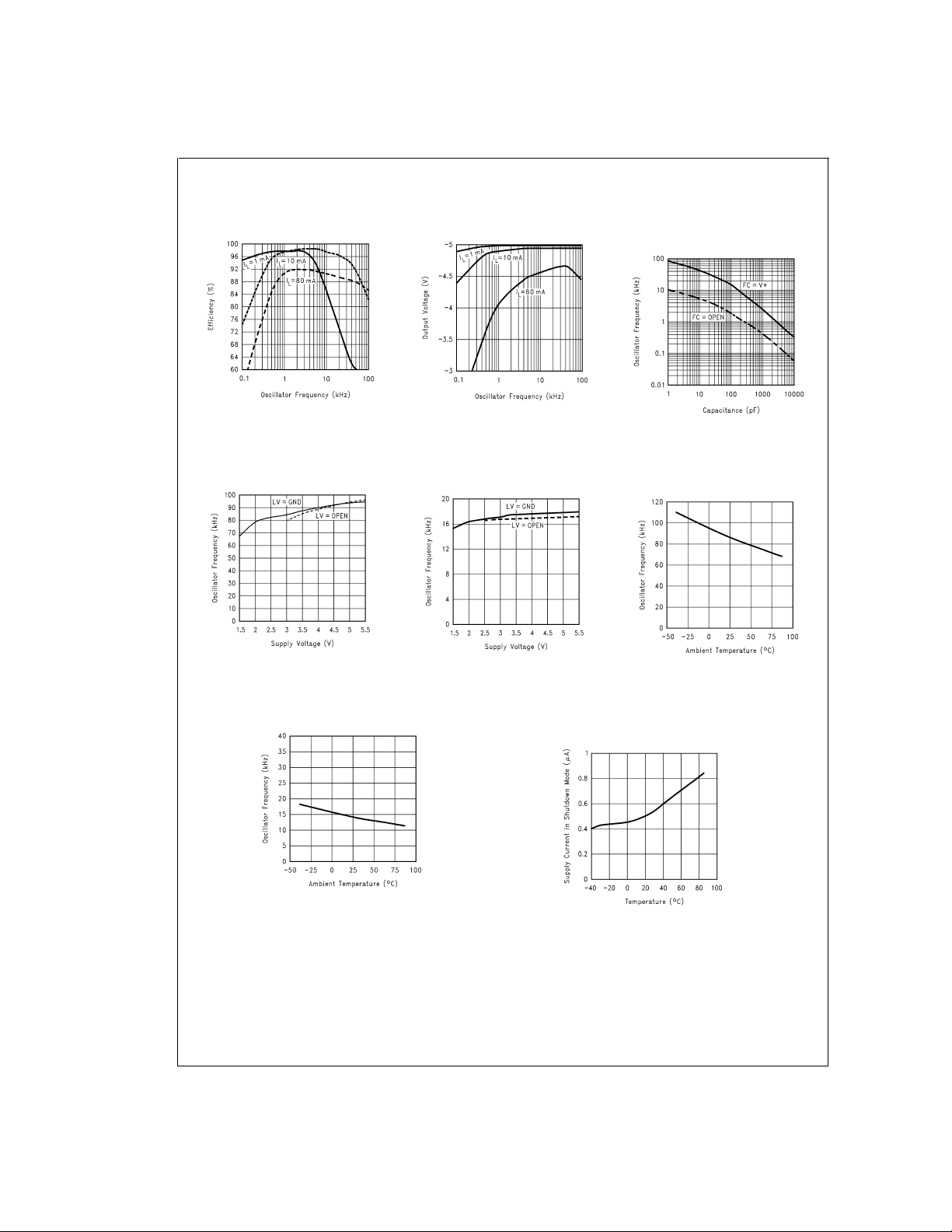
Typical Performance Characteristics (Circuit of
Figure 1
) (Continued)
Efficiency vs
Oscillator Frequency
LM2660/LM2661
Oscillator Frequency
vs Supply Voltage
(FC=V+)
DS012911-13
DS012911-16
Output Voltage vs
Oscillator Frequency
Oscillator Frequency
vs Supply Voltage
(FC=Open)
DS012911-14
DS012911-17
Oscillator Frequency
vs External
Capacitance
DS012911-15
Oscillator Frequency
vs Temperature
(FC=V+)
DS012911-18
Oscillator Frequency
vs Temperature
(FC=Open)
DS012911-19
www.national.com 4
Shutdown Supply
Current vs
Temperature
(LM2661 Only)
DS012911-20

Connection Diagrams
LM2660/LM2661
8-Lead SO (M) or Mini SO (MM)
DS012911-1
DS012911-2
Top View
Order Number LM2660M, LM2661M, LM2660MM or LM2661MM
See NS Package Number M08A and MUA08A
Ordering Information
Order Number Package Number Package Marking Supplied As
LM2660M M08A Datecode Rail (95 units/rail)
LM26
60M
LM2660MX M08A Datecode Tape and Reel (2500 units/rail)
LM26
60M
LM2660MM MUA08A S01A (Note 9) Tape and Reel (250 units/rail)
LM2660MMX MUA08A S01A (Note 9) Tape and Reel (3500 units/rail)
LM2661M M08A Datecode Rail (95 units/rail)
LM26
61M
LM2661MX M08A Datecode Tape and Reel (2500 units/rail)
LM26
61M
LM2661MM MUA08A S02A (Note 9) Tape and Reel (250 units/rail)
LM2661MMX MUA08A S02A (Note 9) Tape and Reel (3500 units/rail)
Note 9: The first letter “S” identifies the part as a switched capacitor converter. The next two numbers are the device number: “01” for a LM2660 device, and “02”
for a LM2661 device. The fourth letter “A” indicates the grade. Only one grade is available. Larger quantity reels are available upon request.
www.national.com5

Pin Description
Pin Name Function
Voltage Inverter Voltage Doubler
1 FC Frequency control for internal oscillator: Same as inverter.
LM2660/LM2661
(LM2660) FC=open, f
FC=V+, f
FC has no effect when OSC pin is driven externally.
1SD
(LM2661)
Shutdown control pin, tie this pin to the ground in
normal operation, and to V+ for shutdown.
2 CAP+ Connect this pin to the positive terminal of
charge-pump capacitor.
3 GND Power supply ground input. Power supply positive voltage input.
4 CAP− Connect this pin to the negative terminal of
charge-pump capacitor.
5 OUT Negative voltage output. Power supply ground input.
6 LV Low-voltage operation input. Tie LV to GND when
input voltage is less than 3.5V. Above 3.5V, LV can
be connected to GND or left open. When driving
OSC with an external clock, LV must be connected
to GND.
7 OSC Oscillator control input. OSC is connected to an
internal 15 pF capacitor. An external capacitor can
be connected to slow the oscillator. Also, an
external clock can be used to drive OSC.
8 V+ Power supply positive voltage input. Positive voltage output.
OSC
OSC
=
10 kHz (typ);
=
80 kHz (typ);
Same as inverter.
Same as inverter.
Same as inverter.
LV must be tied to OUT.
Same as inverter except that OSC cannot be driven
by an external clock.
Circuit Description
The LM2660/LM2661 contains four large CMOS switches
which are switched in a sequence to invert the input supply
voltage. Energy transfer and storage are provided by external capacitors.
scheme. When S
ply voltage V+. During this time interval switches S
are open. In the second time interval, S1and S3are open
and S
2
of cycles, the voltage across C
the anode of C
cathode of C
in the switches, and no ESR in the capacitors. In reality, the
charge transfer efficiency depends on the switching frequency, the on-resistance of the switches, and the ESR of
the capacitors.
Figure 2
illustrates the voltage conversion
and S3are closed, C1charges to the sup-
1
2
and S
and S4are closed, C1is charging C2. After a number
will be pumped to V+. Since
is connected to ground, the output at the
2
equals −(V+) assuming no load on C2, no loss
2
2
DS012911-21
FIGURE 2. Voltage Inverting Principle
Application Information
SIMPLE NEGATIVE VOLTAGE CONVERTER
The main application of LM2660/LM2661 is to generate a
negative supply voltage. The voltage inverter circuit uses
only two external capacitors as shown in the Basic Application Circuits. The range of the input supply voltage is 1.5V to
4
5.5V.For a supply voltage less than 3.5V, the LV pin must be
connected to ground to bypass the internal regulator circuitry. This gives the best performance in low voltage applications. If the supply voltage is greater than 3.5V,LVmay be
connected to ground or left open. The choice of leaving LV
open simplifies the direct substitution of the LM2660/
LM2661 for the LMC7660 Switched Capacitor Voltage Converter.
The output characteristics of this circuit can be approximated
by an ideal voltage source in series with a resistor. The voltage source equals −(V+). The output resistance R
function of the ON resistance of the internal MOS switches,
the oscillator frequency, and the capacitance and ESR of C
and C2. A good approximation is:
where RSWis the sum of the ON resistance of the internal
MOS switches shown in
High value, low ESR capacitors will reduce the output resistance. Instead of increasing the capacitance, the oscillator
frequency can be increased to reduce the 2/(f
Once this term is trivial compared with R
ther increasing in oscillator frequency and capacitance will
become ineffective.
Figure 2
.
oscxC1
and ESRs, fur-
SW
out
) term.
is a
1
www.national.com 6

Application Information (Continued)
The peak-to-peak output voltage ripple is determined by the
oscillator frequency, and the capacitance and ESR of the
output capacitor C
Again, using a low ESR capacitor will result in lower ripple.
POSITIVE VOLTAGE DOUBLER
The LM2660/LM2661 can operate as a positive voltage doubler (as shown in the Basic Application Circuits). The doubling function is achieved by reversing some of the connections to the device. The input voltage is applied to the GND
pin with an allowable voltage from 2.5V to 5.5V. The V+ pin
is used as the output. The LV pin and OUT pin must be connected to ground. The OSC pin can not be driven by an external clock in this operation mode. The unloaded output
voltage is twice of the input voltage and is not reduced by the
diode D
’s forward drop.
1
The Schottky diode D
nal oscillator circuit uses the V+ pin and the LV pin (connected to ground in the voltage doubler circuit) as its power
rails. Voltage across V+ and LV must be larger than 1.5V to
insure the operation of the oscillator. During start-up, D
used to charge up the voltage at V+ pin to start the oscillator;
also, it protects the device from turning-on its own parasitic
diode and potentially latching-up. Therefore, the Schottky diode D
should have enough current carrying capability to
1
charge the output capacitor at start-up, as well as a low forward voltage to prevent the internal parasitic diode from
turning-on. A Schottky diode like 1N5817 can be used for
most applications. If the input voltage ramp is less than 10V/
ms, a smaller Schottky diode like MBR0520LT1 can be used
to reduce the circuit size.
SPLIT V+ IN HALF
Another interesting application shown in the Basic Application Circuits is using the LM2660/LM2661 as a precision voltage divider. Since the off-voltage across each switch equals
V
/2, the input voltage can be raised to +11V.
IN
CHANGING OSCILLATOR FREQUENCY
For the LM2660, the internal oscillator frequency can be selected using the Frequency Control (FC) pin. When FC is
open, the oscillator frequency is 10 kHz; when FC is connected to V+, the frequency increases to 80 kHz. A higher
oscillator frequency allows smaller capacitors to be used for
equivalent output resistance and ripple, but increases the
typical supply current from 0.12 mA to 1 mA.
The oscillator frequency can be lowered by adding an external capacitor between OSC and GND. (See Typical Performance Characteristics.) Also, in the inverter mode, an external clock that swings within 100 mV of V+ and GND can be
used to drive OSC. Any CMOS logic gate is suitable for driving OSC. LV must be grounded when driving OSC. The
maximum external clock frequency is limited to 150 kHz.
The switching frequency of the converter (also called the
charge pump frequency) is half of the oscillator frequency.
Note: OSC cannot be driven by an external clock in the voltage-doubling
mode.
:
2
is only needed for start-up. The inter-
1
1
TABLE 1. LM2660 Oscillator Frequency Selection
FC OSC Oscillator
Open Open 10 kHz
V+ Open 80 kHz
Open or V+ External Capacitor See Typical
N/A External Clock External Clock
(inverter mode only) Frequency
TABLE 2. LM2661 Oscillator Frequency Selection
OSC Oscillator
Open 80 kHz
External Capacitor See Typical Performance
Characteristics
External Clock External Clock Frequency
(inverter mode only)
SHUTDOWN MODE
For the LM2661, a shutdown (SD) pin is available to disable
the device and reduce the quiescent current to 0.5 µA. Applying a voltage greater than 2V to the SD pin will bring the
is
device into shutdown mode. While in normal operating
mode, the SD pin is connected to ground.
CAPACITOR SELECTION
As discussed in the
Simple Negative Voltage Converter
tion, the output resistance and ripple voltage are dependent
on the capacitance and ESR values of the external capacitors. The output voltage drop is the load current times the
output resistance, and the power efficiency is
Where IQ(V+) is the quiescent power loss of the IC device,
2
and I
R
is the conversion loss associated with the
L
OUT
switch on-resistance, the two external capacitors and their
ESRs.
Since the switching current charging and discharging C
approximately twice as the output current, the effect of the
ESR of the pumping capacitor C
output resistance. The output capacitor C
is multiplied by four in the
1
discharging at a current approximately equal to the output
current, therefore, its ESR only counts once in the output resistance. However, the ESR of C
voltage ripple. Therefore, low ESR capacitors (
directly affects the output
2
recommended for both capacitors to maximize efficiency, reduce the output voltage drop and voltage ripple. For convenience, C
and C2are usually chosen to be the same.
1
The output resistance varies with the oscillator frequency
and the capacitors. In
Figure 3
, the output resistance vs. oscillator frequency curves are drawn for three different tantalum capacitors. At very low frequency range, capacitance
plays the most important role in determining the output resistance. Once the frequency is increased to some point (such
as 20 kHz for the 150 µF capacitors), the output resistance is
dominated by the ON resistance of the internal switches and
the ESRs of the external capacitors. A low value, smaller
Performance
Characteristics
is charging and
2
Table 3
sec-
1
) are
LM2660/LM2661
is
www.national.com7

Application Information (Continued)
size capacitor usually has a higher ESR compared with a
bigger size capacitor of the same type. For lower ESR, use
ceramic capacitors.
LM2660/LM2661
FIGURE 3. Output Source Resistance vs Oscillator Frequency
TABLE 3. Low ESR Capacitor Manufacturers
Manufacturer Phone FAX Capacitor Type
Nichicon Corp. (708)-843-7500 (708)-843-2798 PL, PF series, through-hole aluminum electrolytic
AVX Corp. (803)-448-9411 (803)-448-1943 TPS series, surface-mount tantalum
Sprague (207)-324-4140 (207)-324-7223 593D, 594D, 595D series, surface-mount tantalum
Sanyo (619)-661-6835 (619)-661-1055 OS-CON series, through-hole aluminum electrolytic
DS012911-32
Other Applications
PARALLELING DEVICES
Any number of LM2660s (or LM2661s) can be paralleled to reduce the output resistance. Each device must have its own pumping
capacitor C
www.national.com 8
, while only one output capacitor C
1
FIGURE 4. Lowering Output Resistance by Paralleling Devices
is needed as shown in
out
Figure 4
. The composite output resistance is:
DS012911-22

Other Applications (Continued)
CASCADING DEVICES
Cascading the LM2660s (or LM2661s) is an easy way to produce a greater negative voltage (as shown in
integer representing the number of devices cascaded, the unloaded output voltage V
is equal to the weighted sum of each individual device:
is (−nVin). The effective output resistance
out
Figure 5
LM2660/LM2661
). If n is the
A three-stage cascade circuit shown in
Cascading is also possible when devices are operating in doubling mode. In
An example of using the circuit in
Figure 6
generates −3Vin, from Vin.
Figure 6orFigure 7
Figure 7
, two devices are cascaded to generate 3Vin.
is generating +15V or −15V from a +5V input.
Note that, the number of n is practically limited since the increasing of n significantly reduces the efficiency and increases the output resistance and output voltage ripple.
DS012911-23
FIGURE 5. Increasing Output Voltage by Cascading Devices
FIGURE 6. Generating −3Vinfrom +V
FIGURE 7. Generating +3Vinfrom +V
DS012911-24
in
DS012911-25
in
www.national.com9

Other Applications (Continued)
REGULATING V
It is possible to regulate the output of the LM2660/LM2661 by use of a low dropout regulator (such as LP2951). The whole converter is depicted in
LM2660/LM2661
out
Figure 8
. This converter can give a regulated output from −1.5V to −5.5V by choosing the proper resistor ratio:
where, V
=
V
1.235
ref
The error flag on pin 5 of the LP2951 goes low when the regulated output at pin 4 drops by about 5%. The LP2951 can be shutdown by taking pin 3 high.
DS012911-27
FIGURE 8. Combining LM2660/LM2661 with LP2951 to Make a Negative Adjustable Regulator
Also, as shown in
Figure 9
by operating LM2660/LM2661 in voltage doubling mode and adding a linear regulator (such as
LP2981) at the output, we can get +5V output from an input as low as +3V.
FIGURE 9. Generating +5V from +3V Input Voltage
www.national.com 10
DS012911-28

Physical Dimensions inches (millimeters) unless otherwise noted
LM2660/LM2661
Order Number LM2660M or LM2661M
8-Lead SO (M)
NS Package Number M08A
www.national.com11

Physical Dimensions inches (millimeters) unless otherwise noted (Continued)
LM2660/LM2661 Switched Capacitor Voltage Converter
Order Number LM2660MM or LM2661MM
LIFE SUPPORT POLICY
NATIONAL’S PRODUCTS ARE NOT AUTHORIZED FOR USE AS CRITICAL COMPONENTS IN LIFE SUPPORT
DEVICES OR SYSTEMS WITHOUT THE EXPRESS WRITTEN APPROVAL OF THE PRESIDENT AND GENERAL
COUNSEL OF NATIONAL SEMICONDUCTOR CORPORATION. As used herein:
1. Life support devices or systems are devices or
systems which, (a) are intended for surgical implant
into the body, or (b) support or sustain life, and
whose failure to perform when properly used in
accordance with instructions for use provided in the
labeling, can be reasonably expected to result in a
significant injury to the user.
National Semiconductor
Corporation
Americas
Tel: 1-800-272-9959
Fax: 1-800-737-7018
Email: support@nsc.com
www.national.com
National does not assume any responsibility for use of any circuitry described, no circuit patent licenses are implied and National reserves the right at any time without notice to change said circuitry and specifications.
National Semiconductor
Europe
Fax: +49 (0) 1 80-530 85 86
Email: europe.support@nsc.com
Deutsch Tel: +49 (0) 1 80-530 85 85
English Tel: +49 (0) 1 80-532 78 32
Français Tel: +49 (0) 1 80-532 93 58
Italiano Tel: +49 (0) 1 80-534 16 80
8-Lead Mini SO (MM)
NS Package Number MUA08A
2. A critical component is any component of a life
support device or system whose failure to perform
can be reasonably expected to cause the failure of
the life support device or system, or to affect its
safety or effectiveness.
National Semiconductor
Asia Pacific Customer
Response Group
Tel: 65-2544466
Fax: 65-2504466
Email: sea.support@nsc.com
National Semiconductor
Japan Ltd.
Tel: 81-3-5639-7560
Fax: 81-3-5639-7507

WWW.ALLDATASHEET.COM
Copyright © Each Manufacturing Company.
All Datasheets cannot be modified without permission.
This datasheet has been download from :
www.AllDataSheet.com
100% Free DataSheet Search Site.
Free Download.
No Register.
Fast Search System.
www.AllDataSheet.com
 Loading...