

January 15, 2008
LM26480
Externally Programmable Dual High-Current Step-Down
DC/DC and Dual Linear Regulators
General Description
The LM26480 is a multi-functional Power Management Unit,
optimized for low-power digital applications. This device integrates two highly efficient 1.5A step-down DC/DC converters
and two 300 mA linear regulators. The LM26480 is offered in
a tiny 4 x 4 x 0.8mm LLP-24 pin package.
Key Specifications
Step-Down DC/DC Converter (Buck)
1.5A output current
■
V
■
■
■
■
■
■
from:
OUT
Buck1 : 0.8V–2.0V @ 1.5A
—
Buck2 : 1.0V–3.3V @ 1.5A
—
Up to 96% efficiency
±3% FB voltage accuracy
2 MHz PWM switching frequency
PWM - PFM automatic mode change under low loads
Automatic soft start
Linear Regulators (LDO)
V
■
■
■
■
of 1.0V–3.5V
OUT
±3% FB voltage accuracy
300 mA output current
25 mV (typ) dropout
Features
Compatible with advanced applications processors and
■
FPGAs
2 LDOs for powering Internal processor functions and I/Os
■
Precision internal reference
■
Thermal overload protection
■
Current overload protection
■
24-lead 4 × 4 × 0.8mm LLP package
■
External Power-On-Reset function for Buck1 and Buck2
■
Undervoltage lock-out detector to monitor input supply
■
voltage
Applications
Core digital power
■
Applications processors
■
Peripheral I/O power
■
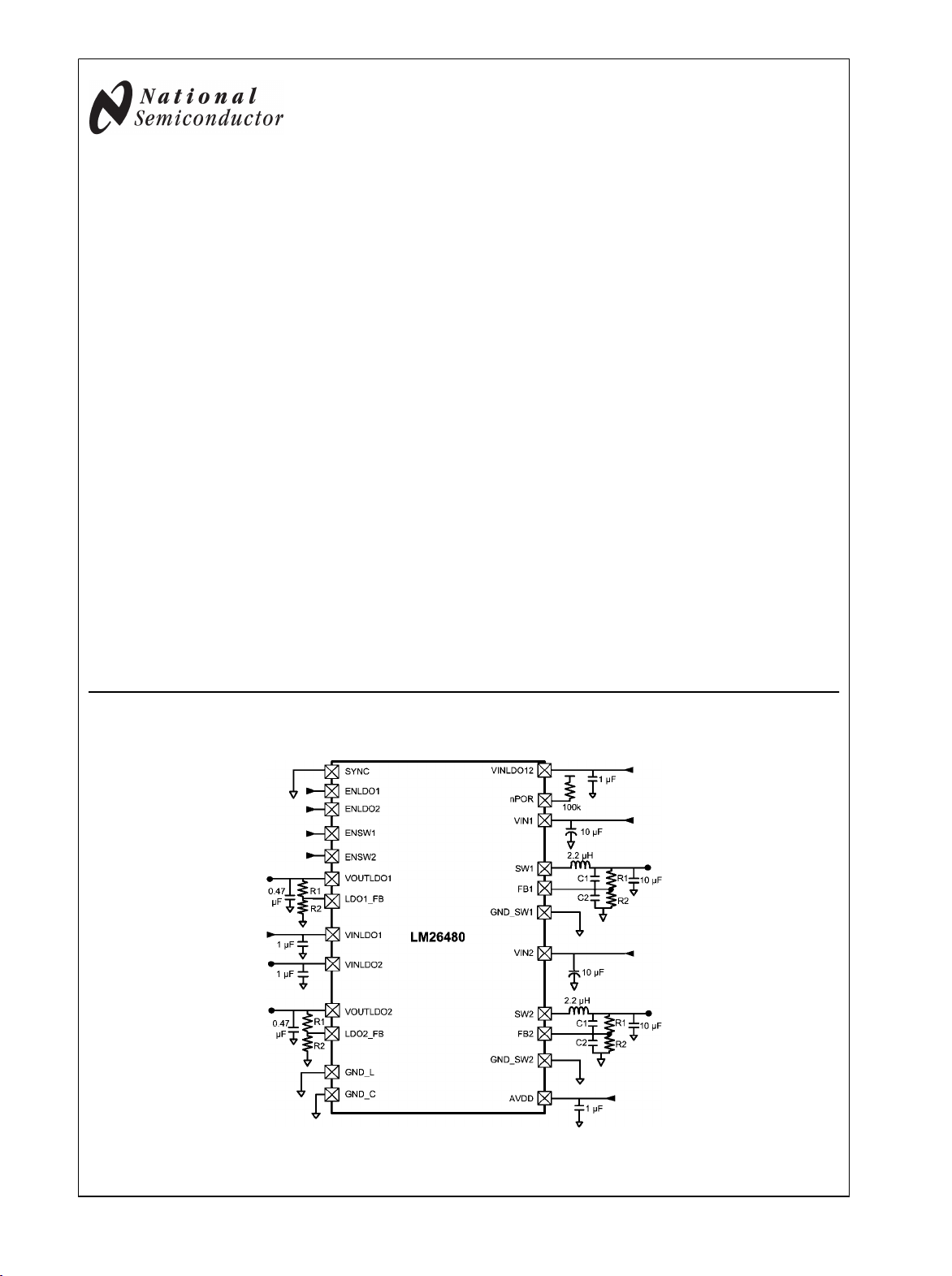
LM26480Externally Programmable Dual High-Current Step-Down DC/DC and Dual Linear
Regulators
Typical Application Circuit
30040401
© 2008 National Semiconductor Corporation 300404 www.national.com
LM26480
FIGURE 1. Application Circuit
www.national.com 2
30040402
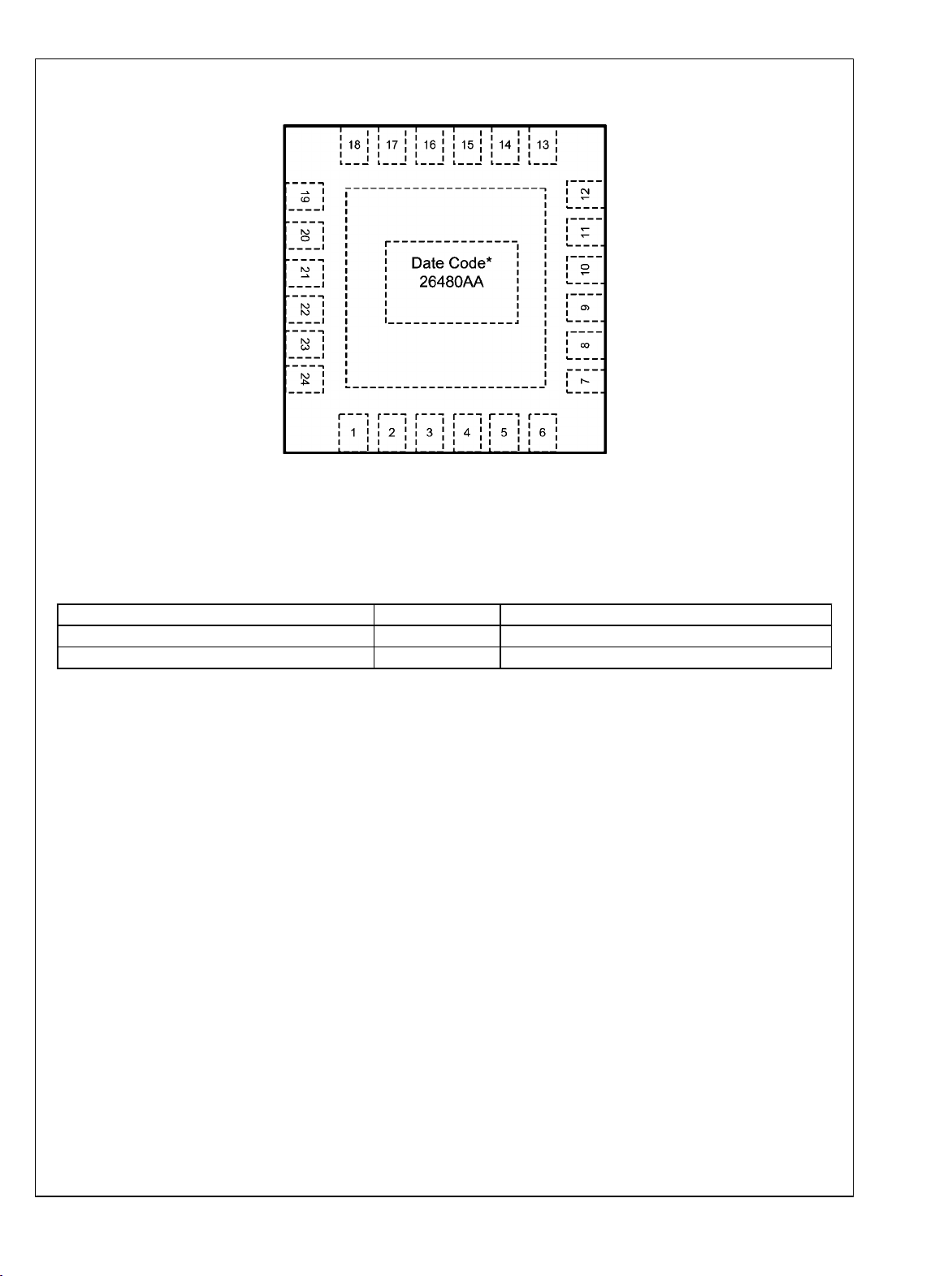
Connection Diagrams and Package Mark Information
30040403
FIGURE 2. 24-Lead LLP Package (top view)
LM26480
Note:
The physical placement of the package marking will vary from part to part.
(*) UZXYTT format: ‘U’ – wafer fab code; ‘Z’ – assembly code; ’XY’ 2 digit date code; ‘TT” – die run code. See http://www.national.com/quality/
marking_conventions.html for more information on marking information.
Part Number Spec Quantity
LM26480SQ-AA NOPB 1000 tape and reel
LM26480SQX-AA NOPB 4500 tape and reel
3 www.national.com
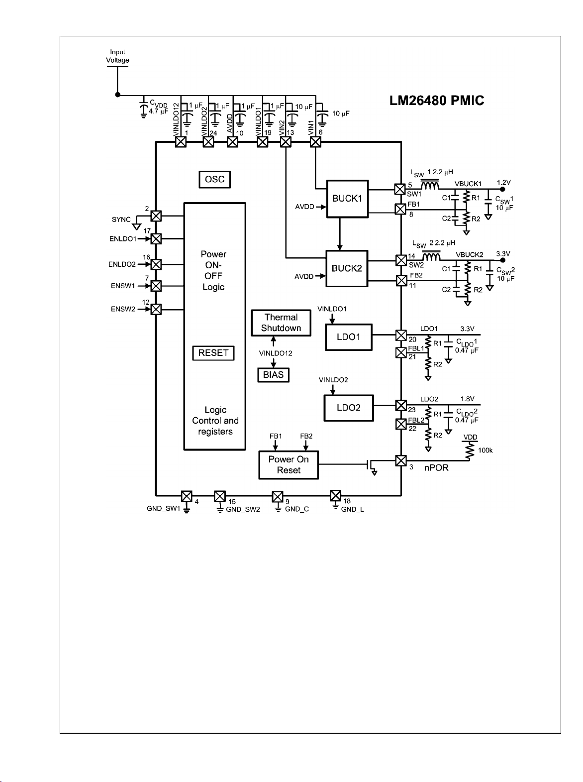
Pin Descriptions
LM26480
LLP Pin No. Name I/O Type Description
1 VINLDO12 I PWR Analog Power for Internal Functions (VREF, BIAS, I2C, Logic)
2 SYNC I G/(D) Frequency Synchronization pin which allows the user to connect an
external clock signal to synchronize the PMIC internal oscillator.
Default OFF and must be grounded when not used. Contact National
Sales office to enable.
3 NPOR O D nPOR Power on reset pin for both Buck1 and Buck 2. Open drain logic
output 100K pullup resistor. nPOR is pulled to ground when the
voltages on these supplies are not good. See nPOR section for more
info.
4 GND_SW1 G G Buck1 NMOS Power Ground
5 SW1 O PWR Buck1 switcher output pin
6 VIN1 I PWR Power in from either DC source or Battery to Buck1
7 ENSW1 I D Enable Pin for Buck1 switcher, a logic HIGH enables Buck1. Pin cannot
be left floating.
8 FB1 I A Buck1 input feedback terminal
9 GND_C G G Non-switching core ground pin
10 AVDD I PWR Analog Power for Buck converters
11 FB2 I A Buck2 input feedback terminal
12 ENSW2 I D Enable Pin for Buck2 switcher, a logic HIGH enables Buck2. Pin cannot
be left floating.
13 VIN2 I PWR Power in from either DC source or Battery to Buck2
14 SW2 O PWR Buck2 switcher output pin
15 GND_SW2 G G Buck2 NMOS
16 ENLDO2 I D LDO2 enable pin, a logic HIGH enables LDO2. Pin cannot be left
floating.
17 ENLDO1 I D LDO1 enable pin, a logic HIGH enables LDO1. Pin cannot be left
floating.
18 GND_L G G LDO ground
19 VINLDO1 I PWR Power in from either DC source or battery to LDO1
20 LDO1 O PWR LDO1 Output
21 FBL1 I A LDO1 Feedback Terminal
22 FBL2 I A LDO2 Feedback Terminal
23 LDO2 O PWR LDO Output
24 VINLDO2 I PWR Power in from either DC source or battery to LDO2.
A: Analog Pin D: Digital Pin G: Ground Pin PWR: Power Pin I: Input Pin I/O: Input/Output Pin O: Output Pin
Power Block Operation Note
Power Block Input Enabled Disabled
VINLDO12 VIN+ VIN+ Always Powered
AVDD VIN+ VIN+ Always Powered
VIN1 VIN+ VIN+ or 0V
VIN2 VIN+ VIN+ or 0V
VINLDO1 ≤ VIN+ ≤ VIN+ If Enabled, Min VIN is 1.74V
VINLDO2 ≤ VIN+ ≤ VIN+ If Enabled, Min VIN is 1.74V
VIN+ is the largest potential voltage on the device.
www.national.com 4
LM26480
Absolute Maximum Ratings (Notes 1, 2)
If Military/Aerospace specified devices are required,
please contact the National Semiconductor Sales Office/
Distributors for availability and specifications.
VINLDO12, VIN1, AVDD, VIN2,
VINLDO1, VINLDO2, ENSW1,
FB1, FB2, ENSW2, ENLDO1,
Operating Ratings: Bucks (Notes 1, 2, 7)
V
IN
V
EN
Junction Temperature (TJ) Range –40°C to +125°C
Ambient Temperature (TA) Range
(Note 6)
2.8V to 5.5V
0 to (VIN + 0.3V)
−40°C to +85°C
ENLDO2, SYNC, FBL1, FBL2 −0.3V to +6V
GND to GND SLUG ±0.3V
Power Dissipation (P
(TA=85°C, T
=125°C ) (Note 5)
MAX
Junction Temperature (T
D_MAX
)
J-MAX
1.17W
)
150°C
Thermal Properties (Notes 3, 5, 6)
Junction-to-Ambient Thermal
Resistance (θJA) SQA024AG
34.1°C/W
Storage Temperature Range −65°C to +150°C
Maximum Lead Temperature (Soldering) 260°C
ESD Ratings
Human Body Model (Note 4) 2 kV
General Electrical Characteristics (Notes 1, 2, 7, 13, 16)
Unless otherwise noted, VIN = 3.6V. Typical values and limits appearing in normal type apply for TJ = 25°C. Limits appearing in
boldface type apply over the entire junction temperature range for operation, −40°C to +125°C.
Symbol Parameter Conditions Min Typ Max Units
I
Q
V
POR
T
SD
T
SDH
UVLO Under Voltage Lock Out Rising 2.9 V
VINLDO12 Shutdown Current VIN = 3.6V
Power-On Reset Threshold VDD Falling Edge(Note 16)
Thermal Shutdown Threshold (Note 13)
Themal Shutdown Hysteresis (Note 13)
Failing 2.7 V
0.5 µA
1.9 V
160 °C
20 °C
Low Drop Out Regulators, LDO1 and LDO2
Unless otherwise noted, VIN = 3.6V, CIN = 1.0 µF, C
TJ = 25°C. Limits appearing in boldface type apply over the entire junction temperature range for operation, −40°C to +125°C.
(Notes 2, 7, 8, 9)
Symbol Parameter Conditions Min Typ Max Units
V
V
ΔV
IN
FB
OUT
Operational Voltage Range VINLDO1 and VINLDO2 PMOS
FB Voltage Accuracy
Line Regulation VIN = (V
Load Regulation VIN = 3.6V,
I
SC
VIN – V
OUT
Short Circuit Current Limit LDO1-2, V
Dropout Voltage Load Current = 50 mA
PSRR Power Supply Ripple Rejection F = 10 kHz, Load Current = I
θn
I
Q
Supply Output Noise 10 Hz < F < 100 kHz
Quiescent Current “On” I
Quiescent Current “On” I
Quiescent Current “Off” EN is de-asserted 0.03 1 µA
T
ON
Turn On Time Start up from shut-down
= 0.47 µF. Typical values and limits appearing in normal type apply for
OUT
pins (Note 15)
1.74 5.5 V
−3 3 %
+ 0.3V) to 5.0V
OUT
(Note 12) Load Current = 1 mA
Load Current = 1 mA to I
= 0V
OUT
MAX
(Note 10)
MAX
0.15 %/V
0.011 %/mA
500 mA
25 200 mV
45 dB
150 µVrms
OUT
OUT
= 0 mA
= 200
40 150 µA
60 200 µA
300 µsec
5 www.national.com
Symbol Parameter Conditions Min Typ Max Units
C
OUT
LM26480
Output Capacitor Capacitance for stability
0°C ≤ TJ ≤ 125°C
−40°C ≤ TJ ≤ 125°C
ESR (Equivalent Series
Resistance)
0.33 0.47 µF
0.68 1.0 µF
5 500
Buck Converters SW1, SW2
Unless otherwise noted, VIN = 3.6V, CIN = 10 µF, C
apply for TJ = 25°C. Limits appearing in boldface type apply over the entire junction temperature range for operation, −40°C to
+125°C. ((Notes 2, 7, 8, 9, 11, 14)
Symbol Parameter Conditions Min Typ Max Units
VFB (Note 14) Feedback Voltage −3 +3 %
V
OUT
Line Regulation 2.8 < VIN < 5.5
Load Regulation 100 mA < IO < I
Eff Efficiency Load Current = 250 mA 96 %
I
SHDN
f
OSC
I
PEAK
Shutdown Supply Current EN is de-asserted 0.01 1 µA
Internal Oscillator Frequency 2.0 2.4 MHz
Buck1 Peak Switching Current Limit 2.0 2.4
Buck2 Peak Switching Current Limit 2.0 2.4
I
Q
R
(P) Pin-Pin Resistance PFET 200 400
DSON
R
(N) Pin-Pin Resistance NFET 180 400
DSON
T
ON
C
IN
C
O
Quiescent Current “On” No load PFM Mode 33 µA
Turn On Time Start up from shut-down 500 µsec
Input Capacitor Capacitance for stability 10 µF
Output Capacitor Capacitance for stability 10 µF
= 10 µF, L
OUT
IO =10 mA
= 2.2 µH. Typical values and limits appearing in normal type
OUT
0.089 %/V
MAX
0.0013 %/mA
mΩ
A
mΩ
mΩ
I/O Electrical Characteristics
Unless otherwise noted: Typical values and limits appearing in normal type apply for TJ = 25°C. Limits appearing in boldface
type apply over the entire junction temperature range for operation, TJ = 0°C to +125°C.
Symbol Parameter Conditions
V
IL
V
IH
Input Low Level
Input High Level
0.7*VDD V
Limit
Min Max
0.4 V
Units
Power On Reset Threshold/Function (POR)
Symbol Parameter Conditions Min Typ Max Units
nPOR nPOR = Power on reset for Buck1 and
Buck2
nPOR
Threshold
V
OL
Percentage of Target voltage Buck1 or
Buck2
Output Level Low Load = IOL = 500 µA 0.23 0.5 V
Default 60 msec
V
BUCK1
V
BUCK1
AND V
OR V
BUCK2
BUCK2
rising
falling
92
82
%
www.national.com 6

Note 1: Absolute Maximum Ratings indicate limits beyond which damage to the component may occur. Operating Ratings are conditions under which operation
of the device is guaranteed. Operating Ratings do not imply guaranteed performance limits. For guaranteed performance limits and associated test conditions,
see the Electrical Characteristics.
Note 2: All voltages are with respect to the potential at the GND pin.
Note 3: Internal thermal shutdown circuitry protects the device from permanent damage. Thermal shutdown engages at TJ = 160°C (typ.) and disengages at T
= 140°C (typ.)
Note 4: The Human body model is a 100 pF capacitor discharged through a 1.5 kΩ resistor into each pin. (MILSTD - 883 3015.7)
Note 5: In applications where high power dissipation and/or poor package thermal resistance is present, the maximum ambient temperature may have to be
derated. Maximum ambient temperature (T
dissipation of the device in the application (P
following equation: T
A-MAX
= T
J-MAX-OP
− (θJA × P
) is dependent on the maximum operating junction temperature (T
A-MAX
), and the junction-to-ambient thermal resistance of the part/package in the application (θJA), as given by the
D-MAX
). See Applications section.
D-MAX
= 125°C), the maximum power
J-MAX-OP
Note 6: Junction-to-ambient thermal resistance is highly application and board-layout dependent. In applications where high maximum power dissipation exists,
special care must be paid to thermal dissipation issues in board design.
Note 7: Min and Max limits are guaranteed by design, test, or statistical analysis. Typical numbers are not guaranteed, but do represent the most likely norm.
Note 8: CIN, C
: Low-ESR Surface-Mount Ceramic Capacitors (MLCCs) used in setting electrical characteristics.
OUT
Note 9: The device maintains a stable, regulated output voltage without a load.
Note 10: Dropout voltage is the voltage difference between the input and the output at which the output voltage drops to 100 mV below its nominal value.
Note 11: Quiescent current is defined here as the difference in current between the input voltage source and the load at V
OUT
.
Note 12: VIN minimum for line regulation values is 1.8V.
Note 13: This specification is guaranteed by design.
Note 14: VIN ≥ V
OUT
+ R
DSON
(P) (I
OUT
+ 1/2 I
). If these conditions are not met, voltage regulation will degrade as load increases.
RIPPLE
Note 15: Pins 24, 19 can operate from VIN min of 1.74V to a VIN max of 5.5V. This rating is only for the series pass PMOS power FET. It allows the system design
to use a lower voltage rating if the input voltage comes from a buck output.
Note 16: VPOR is voltage at which the EPROM resets. This is different from the UVLO on VINLDO12, which is the voltage at which the regulators shut off; and
is also different from the nPOR function, which signals if the regulators are in a specified range.
LM26480
J
7 www.national.com
Typical Performance Characteristics — LDO
LM26480
Output Voltage Change vs Temperature (LDO1)
VIN = 3.6V, V
= 2.5V, 100 mA load
OUT
30040466
Load Transient
3.6 VIN, 2.5V
, 0 – 150 mA load
OUT
Output Voltage Change vs Temperature (LDO2)
VIN = 3.6V, V
= 1.8V, 100 mA load
OUT
30040455
Load Transient
3.6 VIN, 2.5V
, 150–300 mA load
OUT
30040437
Line Transient (LDO1)
3.6 - 4.2 VIN, 2.5 V
www.national.com 8
, 100 mA load
OUT
30040439
Line Transient (LDO2)
3.6 – 4.2 VIN, 1.8V
, 150 mA load
OUT
30040438
30040440
LM26480
Enable Start-up time (LDO1)
0-3.6 VIN, 2.5 V
, 1 mA load
OUT
30040441
Enable Start-up time (LDO2)
0 – 3.6 VIN, 1.8V
, 1 mA load
OUT
30040442
9 www.national.com

Typical Performance Characteristics — Buck V
= 2.8V to 5.5V, TA = 25°C
IN
LM26480
Shutdown Current vs. Temp
Output Voltage vs. Supply Voltage
(V
= 2.0V)
OUT
30040443
Output Voltage vs. Supply Voltage
(V
= 1.2V)
OUT
Output Voltage vs. Supply Voltage
(V
= 3.0V)
OUT
30040444
30040445
www.national.com 10
30040446

Typical Performance Characteristics — Buck Output Current transitions from PFM mode to PWM
mode for Buck 1
LM26480
Efficiency vs. Output Current
(V
= 1.2V, L = 2.2 µH)
OUT
30040447
Output Current transitions from PWM mode to PFM mode
for Buck 2
Efficiency vs. Output Current
(V
= 3.0V, L = 2.2 µH)
OUT
Efficiency vs. Output Current
(V
= 2.0V, L = 2.2 µH)
OUT
Efficiency vs. Output Current
(V
= 3.5V, L = 2.2 µH)
OUT
30040448
30040449
30040450
11 www.national.com

Typical Performance Characteristics — Buck
LM26480
VIN= 3.6V, TA = 25°C, V
= 1.2V unless otherwise noted
OUT
Load Transient Response
V
= 1.2V (PWM Mode)
OUT
Line Transient Response
VIN = 3.6 – 4.2V, V
= 1.2V, 250 mA load
OUT
30040456
Mode Change by Load Transients
V
= 1.2V (PWM to PFM)
OUT
Line Transient Response
VIN = 3.0 – 3.6V, V
= 3.0V, 250 mA load
OUT
30040457
30040458
Start up into PWM Mode
V
= 1.2V, 1.5A load
OUT
30040460
www.national.com 12
Start up into PWM Mode
V
= 3.0 V, 1.5A load
OUT
30040459
30040461

LM26480
Start up into PFM Mode
V
= 1.2V, 30 mA load
OUT
30040462
Start up into PFM Mode
V
= 3.0V, 30 mA load
OUT
30040470
13 www.national.com

DC/DC Converters
OVERVIEW
LM26480
The LM26480 provides the DC/DC converters that supply the
various power needs of the application by means of two linear
low dropout regulators, LDO1 and LDO2, and two buck converters, SW1 and SW2. The table here under lists the output
characteristics of the various regulators.
Supply Specification
Output
Supply Load
LDO1 analog 1.0 to 3.5 300
LDO2 analog 1.0 to 3.5 300
SW1 digital 0.8 to 2.0 1500
SW2 digital 1.0 to 3.3 1500
LINEAR LOW DROPOUT REGULATORS (LDOs)
LDO1 and LDO2 are identical linear regulators targeting analog loads characterized by low noise requirements. LDO1 and
LDO2 are enabled through the ENLDO pin.
V
OUT
Range (V)
Maximum Output
Current (mA)
I
MAX
turns off the device, offering the lowest current consumption.
PWM or PFM mode is selected automatically or PWM mode
can be forced through the setting of the buck control register.
Both SW1 and SW2 can operate up to a 100% duty cycle
(PMOS switch always on) for low drop out control of the output
voltage. In this way the output voltage will be controlled down
to the lowest possible input voltage.
Additional features include soft-start, under-voltage lock-out,
current overload protection, and thermal overload protection.
CIRCUIT OPERATION DESCRIPTION
A buck converter contains a control block, a switching PFET
connected between input and output, a synchronous rectifying NFET connected between the output and ground
(BCKGND pin) and a feedback path. During the first portion
of each switching cycle, the control block turns on the internal
PFET switch. This allows current to flow from the input
through the inductor to the output filter capacitor and load. The
inductor limits the current to a ramp with a slope of
by storing energy in a magnetic field. During the second portion of each cycle, the control block turns the PFET switch off,
blocking current flow from the input, and then turns the NFET
synchronous rectifier on. The inductor draws current from
ground through the NFET to the output filter capacitor and
load, which ramps the inductor current down with a slope of
30040404
NO-LOAD STABILITY
The LDOs will remain stable and in regulation with no external
load. This is an important consideration in some circuits, for
example, CMOS RAM keep-alive applications.
SW1, SW2: Synchronous StepDown Magnetic DC/DC Converters
FUNCTIONAL DESCRIPTION
The LM26480 incorporates two high-efficiency synchronous
switching buck regulators, SW1 and SW2, that deliver a constant voltage from a single Li-Ion battery to the portable
system processors. Using a voltage mode architecture with
synchronous rectification, both bucks have the ability to deliver up to 1500 mA depending on the input voltage and output
voltage (voltage head room), and the inductor chosen (maximum current capability).
There are three modes of operation depending on the current
required - PWM, PFM, and shutdown. PWM mode handles
current loads of approximately 70 mA or higher, delivering
voltage precision of +/-3% with 90% efficiency or better.
Lighter output current loads cause the device to automatically
switch into PFM for reduced current consumption (IQ = 15 µA
typ.) and a longer battery life. The Standby operating mode
The output filter stores charge when the inductor current is
high, and releases it when low, smoothing the voltage across
the load.
PWM OPERATION
During PWM operation the converter operates as a voltagemode controller with input voltage feed forward. This allows
the converter to achieve excellent load and line regulation.
The DC gain of the power stage is proportional to the input
voltage. To eliminate this dependence, feed forward voltage
inversely proportional to the input voltage is introduced.
INTERNAL SYNCHRONOUS RECTIFICATION
While in PWM mode, the buck uses an internal NFET as a
synchronous rectifier to reduce rectifier forward voltage drop
and associated power loss. Synchronous rectification provides a significant improvement in efficiency whenever the
output voltage is relatively low compared to the voltage drop
across an ordinary rectifier diode.
CURRENT LIMITING
A current limit feature allows the converter to protect itself and
external components during overload conditions. PWM mode
implements current limiting using an internal comparator that
trips at 2.0A for both bucks (typ). If the output is shorted to
ground the device enters a timed current limit mode where the
NFET is turned on for a longer duration until the inductor current falls below a low threshold, ensuring inductor current has
more time to decay, thereby preventing runaway.
www.national.com 14

LM26480
PFM OPERATION
At very light loads, the converter enters PFM mode and operates with reduced switching frequency and supply current
to maintain high efficiency.
The part will automatically transition into PFM mode when either of two conditions occurs for a duration of 32 or more clock
cycles:
A. The inductor current becomes discontinuous
or
B. The peak PMOS switch current drops below the I
level
MODE
During PFM operation, the converter positions the output voltage slightly higher than the nominal output voltage during
PWM operation, allowing additional headroom for voltage
drop during a load transient from light to heavy load. The PFM
comparators sense the output voltage via the feedback pin
and control the switching of the output FETs such that the
output voltage ramps between 0.8% and 1.6% (typical) above
the nominal PWM output voltage. If the output voltage is below the ‘high’ PFM comparator threshold, the PMOS power
switch is turned on. It remains on until the output voltage exceeds the ‘high’ PFM threshold or the peak current exceeds
the I
level set for PFM mode. The typical peak current in
PFM
PFM mode is:
Once the PMOS power switch is turned off, the NMOS power
switch is turned on until the inductor current ramps to zero.
When the NMOS zero-current condition is detected, the
NMOS power switch is turned off. If the output voltage is below the ‘high’ PFM comparator threshold (see following figure), the PMOS switch is again turned on and the cycle is
repeated until the output reaches the desired level. Once the
output reaches the ‘high’ PFM threshold, the NMOS switch is
turned on briefly to ramp the inductor current to zero and then
both output switches are turned off and the part enters an
extremely low power mode. Quiescent supply current during
this ‘sleep’ mode is less than 30 µA, which allows the part to
achieve high efficiencies under extremely light load conditions. When the output drops below the ‘low’ PFM threshold,
the cycle repeats to restore the output voltage to ~1.6% above
the nominal PWM output voltage.
If the load current should increase during PFM mode (see
figure below) causing the output voltage to fall below the
‘low2’ PFM threshold, the part will automatically transition into
fixed-frequency PWM mode.
SW1, SW2 CONTROL
SW1 and SW2 are enabled/disabled through the external enable pins.
The Modulation mode PWM/PFM is by default automatic and
depends on the load as described above in the functional description. The modulation mode can be factory trimmed, forcing the buck to operate in PWM mode regardless of the load
condition.
30040405
15 www.national.com

SHUTDOWN MODE
During shutdown the PFET switch, reference, control and
bias circuitry of the converters are turned off. The NFET
LM26480
switch will be on in shutdown to discharge the output. When
the converter is enabled, soft start is activated. It is recommended to disable the converter during the system power up
and under voltage conditions when the supply is less than
2.8V.
SOFT START
The soft-start feature allows the power converter to gradually
reach the initial steady state operating point, thus reducing
start-up stresses and surges. The two LM26480 buck converters have a soft-start circuit that limits in-rush current during start-up. During start-up the switch current limit is
increased in steps. Soft start is activated only if EN goes from
logic low to logic high after VIN reaches 2.8V. Soft start is implemented by increasing switch current limit in steps of 250
mA, 500 mA, 950 mA and 2A for both bucks (typ. switch current limit). The start-up time thereby depends on the output
capacitor and load current demanded at start-up.
LOW DROPOUT OPERATION
The LM26480 can operate at 100% duty cycle (no switching;
PMOS switch completely on) for low dropout support of the
output voltage. In this way the output voltage will be controlled
down to the lowest possible input voltage. When the device
operates near 100% duty cycle, output voltage ripple is approximately 25 mV. The minimum input voltage needed to
support the output voltage is
V
IN,
—
—
MIN = I
I
LOAD
R
DSON, PFET
LOAD
* (R
DSON, PFET
+ R
Load current
Drain to source resistance of
INDUCTOR
) + V
OUT
PFET switch in the triode region
—
R
INDUCTOR
Inductor resistance
FLEXIBLE POWER-ON RESET (i.e., POWER GOOD WITH DELAY)
The LM26480 is equipped with an internal Power-On-Reset
(“POR”) circuit which monitors the output voltage levels on
bucks 1 and 2. The nPOR is an open drain logic output which
is logic LOW when either of the buck outputs are below 91%
of the rising value , or when one or both outputs fall below
82% of the desired value. The time delay between output
voltage level and nPOR is enabled is (50 µs, 50 ms, 100 ms,
200 ms) 50 ms by default. The system designer can choose
the external pull-up resistor (i.e. 100 kΩ ) for the nPOR pin.
www.national.com 16

NPOR with Counter Delay
LM26480
The above diagram shows the simplest application of the
Power-On Reset, where both switcher enables are tied together. In Case 1, EN1 causes nPOR to transition LOW and
triggers the nPOR delay counter. If the power supply for
Buck2 does not come on within that period, nPOR will stay
LOW, indicating a power fail mode. Case 2 indicates the vice
versa scenario if Buck1 supply did not come on. In both cases
30040406
the nPOR remains LOW. Case 3 shows a typical application
of the Power-On Reset, where both switcher enables are tied
together. Even if RDY1 ramps up slightly faster than RDY2
(or vice versa), the nPOR signal will trigger a programmable
delay before going HIGH, as explained below.
17 www.national.com

LM26480
Faults Occurring in Counter Delay After Startup
The above timing diagram details the Power Good with delay
with respect to the enable signals EN1, and EN2. The RDY1,
RDY2 are internal signals derived from the output of two comparators. Each comparator has been trimmed as follows:
Comparator Level Buck Supply Level
HIGH Greater than 91%
LOW Less than 82%
The circuits for EN1 and RDY1 are symmetrical to EN2 and
RDY2, so each reference to EN1 and RDY1 will also work for
EN2 and RDY2 and vice versa.
If EN1 and RDY1 signals are High at time t1, then the RDY1
30040407
signal rising edge triggers the programmable delay counter
(50 μs, 50 ms, 100 ms, 200 ms). This delay forces nPOR LOW
between time interval t1 and t2. NPOR is then pulled high after
the programmable delay is completed. Now if EN2 and RDY2
are initiated during this interval the nPOR signal ignores this
event.
If either RDY1or RDY2 were to go LOW at t3 then the programmable delay is triggered again.
www.national.com 18

NPOR Mask Window
LM26480
In Case 1, we see that case where EN2 and RDY2 are initiated after triggered programmable delay. To prevent the
nPOR being asserted again, a masked window (5 ms) counter
delay is triggered off the EN2 rising edge. NPOR is still held
HIGH for the duration of the mask, whereupon the nPOR status afterwards will depend on the status of both RDY1 and
RDY2 lines.
In Case 2, we see the case where EN2 is initiated after the
RDY1 triggered programmable delay, but RDY2 never goes
HIGH (Buck2 never turns on). Normal operation operation of
30040408
nPOR occurs wilth respect to EN1 and RDY1, and the nPOR
signal is held HIGH for the duration of the mask window. We
see that nPOR goes LOW after the masking window has
timed out because it is now dependent on RDY1 and RDY2,
where RDY2 is LOW.
19 www.national.com

LM26480
Design Implementation of the Flexible Power-On Reset
Design implementation of the flexible power-on reset. An internal power-on reset of the IC is used with EN1 and EN2 to
produce a reset signal (LOW) to the delay timer nPOR. EN1
and RDY1 or EN2 and RDY2 are used to generate the set
signal (HIGH) to the delay timer. S=R=1 never occurs. The
mask timers are triggered off EN1 and EN2 which are gated
with RDY1, and RDY2 to generate outputs to the final AND
gate to generate the nPOR.
UNDER VOLTAGE LOCK OUT
The LM26480 features an “under voltage lock out circuit”. The
function of this circuit is to continuously monitor the raw input
supply voltage (VINLDO12) and automatically disables the
30040409
four voltage regulators whenever this supply voltage is less
than 2.8 VDC.
The circuit incorporates a bandgap based circuit that establishes the reference used to determine the 2.8 VDC trip point
for a VIN OK – Not OK detector. This VIN OK signal is then
used to gate the enable signals to the four regulators of the
LM26480. When VINLDO12 is greater than 2.8 VDC the four
enables control the four regulators, when VINLDO12 is less
than 2.8 VDC the four regulators are disabled by the VIN detector being in the “Not OK” state. The circuit has built in
hysteresis to prevent chattering occurring.
www.national.com 20

Application Notes
EXTERNAL COMPONENT SELECTION
LM26480
30040410
Ideal Resistor Values Common R Values Feedback Capacitors
Target
Vout (V)
R1 (KΩ) R2 (KΩ) R1 (KΩ) R2 (KΩ)
Actual V
Com/R (V)
OUT
W/
Actual
V
Delta from
OUT
Target (V)
C1(pF) C2(pF)
0.8 120 200 121 200 0.803 0.002 15 none Buck1
0.9 160 200 162 200 0.905 0.005 15 none Only
1 200 200 200 200 1 0 15 none ^
1.1 240 200 240 200 1.1 0 15 none |
1.2 280 200 280 200 1.2 0 12 none |
1.3 320 200 324 200 1.31 0.01 12 none Buck1
1.4 360 200 357 200 1.393 -0.008 10 none And
1.5 400 200 402 200 1.505 0.005 10 none Buck2
1.6 440 200 442 200 1.605 0.005 8.2 none |
1.7 427 178 432 178 1.713 0.013 8.2 none |
1.8 463 178 464 178 1.803 0.003 8.2 none |
1.9 498 178 499 178 1.902 0.002 8.2 none |
2 450 150 453 150 2.01 0.01 8.2 none >
2.1 480 150 475 150 2.083 -0.017 8.2 none ^
2.2 422 124 422 124 2.202 0.002 8.2 none |
2.3 446 124 442 124 2.282 -0.018 8.2 none |
2.4 471 124 475 124 2.415 0.015 8.2 none |
2.5 400 100 402 100 2.51 0.01 8.2 none |
2.6 420 100 422 100 2.61 0.01 8.2 none |
2.7 440 100 442 100 2.71 0.01 8.2 33 Buck2
2.8 460 100 464 100 2.82 0.02 8.2 33 Only
2.9 480 100 475 100 2.875 -0.025 8.2 33 |
3 500 100 499 100 2.995 -0.005 6.8 33 |
3.1 520 100 523 100 3.115 0.015 6.8 33 |
3.2 540 100 536 100 3.18 -0.02 6.8 33 |
3.3 560 100 562 100 3.31 0.01 6.8 33 |
The output voltages of the bucks of the LM26480 are established by the feed back resistor divider R1 shown on the
application circuit above. The equation for determining V is:
V
= VFB (R1+R2)/R2 where VFB is the voltage on the Buck
OUT
FBx pin.
The Buck control loop will force the voltage on VFB to be 0.50
V +/- 3%.
The above table shows ideal resistor values to establish buck
voltages from 0.8V to 3.3 V along with common resistor val-
ues to establish these voltages. Common resistors do not
always produce the target value, error is given in the delta
column.
In addition to the resistor feedback, capacitor feedback C1 is
always required, and depending on the output voltage capacitor C2 is also required. See the application diagram below
and the above table for these requirements.
21 www.national.com

Inductor Value Unit Description Notes
LSW1,2 2.2 µH SW1,2 inductor
LM26480
OUTPUT INDUCTORS & CAPACITORS FOR SW1 AND SW2
There are several design considerations related to the selection of output inductors and capacitors:
•
Load transient response;
•
Stability;
•
Efficiency;
•
Output ripple voltage; and
•
Over-current ruggedness.
The LM26480 has been optimized for use with nominal values
2.2 µH and 10 µF. If other values are needed for the design,
please contact National Semiconductor sales with any concerns.
INDUCTOR SELECTION FOR SW1 AND SW2
A nominal inductor value of 2.2 µH is recommended. It is important to guarantee the inductor core does not saturate
during any foreseeable operational situation.
Care should be taken when reviewing the different saturation
current ratings that are specified by different manufacturers.
Saturation current ratings are typically specified at 25ºC, so
ratings at maximum ambient temperature of the application
should be requested from the manufacturer.
There are two methods to choose the inductor saturation current rating:
Recommended method:
The best way to guarantee the inductor does not saturate is
to choose an inductor that has saturation current rating
greater than the maximum LM26480 current limit of 2.4A. In
this case the device will prevent inductor saturation.
Alternate method:
If the recommended approach cannot be used, care must be
taken to guarantee that the saturation current is greater than
the peak inductor current:
D.C.R. 70 mΩ
I
may not be exceeded during any operation, including
SAT
transients, startup, high temperature, worst case conditions,
etc.
SUGGESTED INDUCTORS AND THEIR SUPPLIERS
Model Vendor Dimension
s (mm)
DO3314-22
Coilcraft 3.3 x 3.3 x
2MX
LPO3310-2
Coilcraft 3.3 x 3.3 x 1
1.4
DCR
(max)
200 mΩ
150 mΩ
I
SATURATION
≈1.8A
≈1.3A
22MX
ELL6PG2R2NPanaso
nic
ELC6GN2R2NPanaso
nic
CDRH2D14
Sumida 3.2 x 3.2 x
NP-2R2NC
Note: Inductor Current Saturation values are estimates; inductor
manufacturer should be contacted for guaranteed values.
6.0 x 6.0 x
2.0
6.0 x 6.0 x
1.5
1.5
37mΩ
53 mΩ
94 mΩ
≈2.2A
≈1.9A
≈1.5A
OUTPUT CAPACITOR SELECTION FOR SW1 AND SW2
A ceramic output capacitor of 10 µF, 6.3V is recommended
with an ESR of about 2 mΩ or less.
Output ripple can be estimated from the vector sum of the
reactive (Capacitor) voltage component and the real (ESR)
voltage component of the output capacitor.
I
:
SAT
I
LPEAK
I
OUTMAX
I
RIPPLE
V
OUT
VIN:
L:
F:
D:
EFF:
www.national.com 22
Inductor saturation current at operating temperature
:
Peak inductor current during worst case conditions
:
Maximum average inductor current
:
Peak-to-Peak inductor current
:
Output voltage
Input voltage
Inductor value in Henries at I
Switching frequency, Hertz
Estimated duty factor
Estimated power supply efficiency
30040471
OUTMAX
V
:
COUT
V
ROUT
V
PPOUT
Estimated reactive output ripple
:
Estimated real output ripple
:
Estimated peak-to-peak output ripple
The output capacitor needs to be mounted as close as possible to the output pin of the device. For better temperature
performance, X7R or X5R types are recommended. DC bias
characteristics of ceramic capacitors must be considered
when selecting case sizes like 0805 and 0603.
DC bias characteristics vary from manufacturer to manufacturer and by case size. DC bias curves should be requested
from them as part of the capacitor selection process. ESR is
typically higher for smaller packages.
The output filter capacitor smooths out current flow from the
inductor to the load, helps maintain a steady output voltage
during transient load changes and reduces output voltage
ripple. These capacitors must be selected with sufficient capacitance and sufficiently low ESR to perform these functions.
Note that the output voltage ripple is dependent on the inductor current ripple and the equivalent series resistance of the
output capacitor (ESR
dent as well as temperature dependent. The R
calculated with the applicable switching frequency and ambi-
COUT
). ESR
is frequency depen-
COUT
ESR
should be
ent temperature.

INPUT CAPACITOR SELECTION FOR SW1 AND SW2
It is required to use a ceramic input capacitor of at least 4.7
μF and 6.3V with an ESR of under 10 mΩ.
The input power source supplies average current continuously. During the PFET switch on-time, however, the demanded di/dt is higher than can be typically supplied by the
input power source. This delta is supplied by the input capacitor.
A simplified “worst case” assumption is that all of the PFET
current is supplied by the input capacitor. This will result in
conservative estimates of input ripple voltage and capacitor
RMS current. Input ripple voltage is estimated as follows:
V
:
PPIN
I
OUT
C
IN:
ESR
Estimated peak-to-peak input ripple voltage
:
Output current, Amps
Input capacitor value, Farads
Input capacitor ESR, Ohms
IN:
This capacitor is exposed to significant RMS current, so it is
important to select a capacitor with an adequate RMS current
rating. Capacitor RMS current estimated as follows:
LM26480
I
RSCIN
Estimated input capacitor RMS current
Model Type Vendor Voltage Rating Case Size
4.7 µF for CIN
C2012X5R0J475K Ceramic, X5R TDK 6.3V 0805, (2012)
JMK212BJ475K Ceramic, X5R Taiyo-Yuden 6.3V 0805, (2012)
GRM21BR60J475K Ceramic, X5R Murata 6.3V 0805, (2012)
C1608X5R0J475K Ceramic, X5R TDK 6.3V 0603, (1608)
10 µF for COUT
GRM21BR60J106K Ceramic, X5R Murata 6.3V 0805, (2012)
JMK212BJ106K Ceramic, X5R Taiyo-Yuden 6.3V 0805, (2012)
C2012X5R0J106K Ceramic, X5R TDK 6.3V 0805, (2012)
C1608X5R0J106K Ceramic, X5R TDK 6.3V 0603, (1608)
23 www.national.com

FEEDBACK RESISTORS FOR LDOs
LM26480
30040410
Target V
(V) Ideal Resistor Values Common R Values Actual V
OUT
R1 (KΩ) R2 (KΩ) R1 (KΩ) R2 (KΩ)
1 200 200 200 200 1
1.1 240 200 240 200 1.1
1.2 280 200 280 200 1.2
1.3 320 200 324 200 1.31
1.4 360 200 357 200 1.393
1.5 400 200 402 200 1.505
1.6 440 200 442 200 1.605
1.7 480 200 562 232 1.711
1.8 520 200 604 232 1.802
1.9 560 200 562 200 1.905
2 600 200 604 200 2.01
2.1 640 200 715 221 2.118
2.2 680 200 681 200 2.203
2.3 720 200 806 226 2.283
2.4 760 200 845 221 2.412
2.5 800 200 750 187 2.505
2.6 840 200 909 215 2.614
2.7 880 200 1100 249 2.709
2.8 920 200 1150 249 2.809
2.9 960 200 1210 255 2.873
3 1000 200 1000 200 3
3.1 1040 200 1000 191 3.118
3.2 1080 200 1000 187 3.174
3.3 1120 200 1210 215 3.314
3.4 1160 200 1210 210 3.381
3.5 1200 200 1210 200 3.525
OUT
Com/R (V)
W/
The output Voltages of the LDOs of the LM26480 are established by the feed back resistor divider R1 shown on the
application circuit above. The equation for determining V
is: V
= VFB(R1+R2)/R2, where Vfb is the voltage on the
OUT
LDOX_FB pin.
OUT
The LDO control loop will force the voltage on VFBo be 0.50
V +/- 3%. The above table shows ideal resistor values to es-
www.national.com 24
tablish LDO voltages from 1.0 V to 3.5 V along with common
resistor values to establish these voltages. Common resistors
do not always produce the target value, error is given in the
final column.
To keep the power consumed by the feedback network low it
is recommended that R2 be established as about 200 KΩ.
Lesser values of R2 are OK at the users discretion..

LM26480
LDO CAPACITOR SELECTION
Input Capacitor
An input capacitor is required for stability. It is recommended
that a 1.0 μF capacitor be connected between the LDO input
pin and ground (this capacitance value may be increased
without limit). This capacitor must be located a distance of not
more than 1 cm from the input pin and returned to a clean
analog ground. Any good quality ceramic, tantalum, or film
capacitor may be used at the input.
Important: Tantalum capacitors can suffer catastrophic failures due to surge currents when connected to a low
impedance source of power (like a battery or a very large capacitor). If a tantalum capacitor is used at the input, it must be
guaranteed by the manufacturer to have a surge current rating sufficient for the application.
There are no requirements for the ESR on the input capacitor,
but tolerance and temperature coefficient must be considered
when selecting the capacitor to ensure the capacitance will
remain approximately 1.0 μF over the entire operating temperature range.
Output Capacitor
The LDOs on the LM26480 are designed specifically to work
with very small ceramic output capacitors. A 1.0 μF ceramic
capacitor (temperature types Z5U, Y5V or X7R) with ESR between 5 mΩ to 500 mΩ, are suitable in the application circuit.
It is also possible to use tantalum or film capacitors at the
device output COUT (or VOUT), but these are not as attractive for reasons of size and cost. The output capacitor must
meet the requirement for the minimum value of capacitance
and also have an ESR value that is within the range 5 mΩ to
500 mΩ for stability.
Capacitor Characteristics
The LDOs are designed to work with ceramic capacitors on
the output to take advantage of the benefits they offer. For
capacitance values in the range of 0.47 μF to 4.7 μF, ceramic
capacitors are the smallest, least expensive and have the
lowest ESR values, thus making them best for eliminating
high frequency noise. The ESR of a typical 1.0 μF ceramic
capacitor is in the range of 20 mΩ to 40 mΩ, which easily
meets the ESR requirement for stability for the LDOs.
For both input and output capacitors, careful interpretation of
the capacitor specification is required to ensure correct device
operation. The capacitor value can change greatly, depending on the operating conditions and capacitor type.
In particular, the output capacitor selection should take account of all the capacitor parameters, to ensure that the
specification is met within the application. The capacitance
can vary with DC bias conditions as well as temperature and
frequency of operation. Capacitor values will also show some
decrease over time due to aging. The capacitor parameters
are also dependent on the particular case size, with smaller
sizes giving poorer performance figures in general. As an example, the graph below shows a typical graph comparing
different capacitor case sizes in a capacitance vs. DC bias
plot.
30040416
As shown in the graph, increasing the DC bias condition can
result in the capacitance value that falls below the minimum
value given in the recommended capacitor specifications table. Note that the graph shows the capacitance out of spec
for the 0402 case size capacitor at higher bias voltages. It is
therefore recommended that the capacitor manufacturers’
specifications for the nominal value capacitor are consulted
for all conditions, as some capacitor sizes (e.g. 0402) may not
be suitable in the actual application.
The ceramic capacitor’s capacitance can vary with temperature. The capacitor type X7R, which operates over a temperature range of −55°C to +125°C, will only vary the capacitance
to within ±15%. The capacitor type X5R has a similar tolerance over a reduced temperature range of −55°C to +85°C.
Many large value ceramic capacitors, larger than 1 μF are
manufactured with Z5U or Y5V temperature characteristics.
Their capacitance can drop by more than 50% as the temperature varies from 25°C to 85°C. Therefore X7R is recommended over Z5U and Y5V in applications where the ambient
temperature will change significantly above or below 25°C.
Tantalum capacitors are less desirable than ceramic for use
as output capacitors because they are more expensive when
comparing equivalent capacitance and voltage ratings in the
0.47 μF to 4.7 μF range. Another important consideration is
that tantalum capacitors have higher ESR values than equivalent size ceramics. This means that while it may be possible
to find a tantalum capacitor with an ESR value within the stable range, it would have to be larger in capacitance (which
means bigger and more costly) than a ceramic capacitor with
the same ESR value. It should also be noted that the ESR of
a typical tantalum will increase about 2:1 as the temperature
goes from 25°C down to −40°C, so some guard band must
be allowed.
Capacitor Min Value Unit Description Recommended Type
CLDO1 0.47 µF LDO1 output capacitor Ceramic, 6.3V, X5R
CLDO2 0.47 µF LDO2 output capacitor Ceramic, 6.3V, X5R
CSW1 10 µF SW1 output capacitor Ceramic, 6.3V, X5R
CSW2 10 µF SW2 output capacitor Ceramic, 6.3V, X5R
25 www.national.com

Analog Power Signal Routing
All power inputs should be tied to the main VDD source (i.e.
LM26480
battery), unless the user wishes to power it from another
source. (i.e. powering LDO from Buck output).
The analog VDD inputs power the internal bias and error amplifiers, so they should be tied to the main VDD. The analog
VDD inputs must have an input voltage between 2.8 and 5.5
V, as specified in the Electrical Characteristics section of this
datasheet.
The other Vins (VINLDO1, VINLDO2, VIN1, VIN2) can actually have inputs lower than 2.8V, as long as it's higher than
the programmed output (+0.3V, to be safe). The analog and
digital grounds should be tied together outside of the chip to
reduce noise coupling.
For more information on board layout techniques, refer to Application Note AN–1187 “Leadless Lead frame Package
(LLP).” on http://www.national.com This application note also
discusses package handling, solder stencil and the assembly
process.
www.national.com 26

LM26480
Board Layout Considerations
PC board layout is an important part of DC-DC converter design. Poor board layout can disrupt the performance of a DCDC converter and surrounding circuitry by contributing to EMI,
ground bounce, and resistive voltage loss ii the traces. These
can send erroneous signals to the DC-DC converter IC, re-
sulting in poor regulation or instability. Poor layout can also
result in re-flow problems leading to poor solder joints, which
can result in erratic or degraded performance.
Good layout for the LM26480 bucks can be implemented by
following a few simple design rules, as illustrated in Figure 6.
FIGURE 3. Board Layout Design Rules for the LM26480
1.
Place the buck inductor and filter capacitors close
together and make the trace short. The traces between
these components carry relatively high switching
currents and act as antennas. Following this rule reduces
radiated noise. Place the capacitors and inductor close
to the buck.
2.
Arrange the components so that the switching current
loops curl in the same direction. During the first halt of
each cycle, current flows from the input filter capacitor,
through the buck and inductor to the output filter
capacitor and back through ground, forming a current
loop. In the second half of each cycle, current is pulled
up from ground, through the buck by the inductor, to the
output filter capacitor and then back through ground,
forming a second current loop. Routing these loops so
the current curls in the same direction prevents magnetic
field reversal between the two half-cycles and reduces
radiated noise.
3.
Connect the ground pins of the buck, and filter capacitors
together using generous component-side copper fill as a
pseudo-ground plane. Then connect this to the groundplane (if one is used) with several vias. This reduces
ground—plane noise by preventing the switching
currents from circulating through the ground plane. it also
30040468
reduces ground bounce at the buck by giving it a lowimpedance ground connection.
4.
Use wide traces between the power components and for
power connections to the DC-DC converter circuit. This
reduces voltage errors caused by resistive losses across
the traces
5.
Rout noise sensitive traces, such as the voltage
feedback path, away from noisy traces between the
power components. The voltage feedback trace must
remain close to the buck circuit and should be routed
directly from FB to VOUT at the output capacitor and
should be routed opposite to noise components. This
reduces EMI radiated onto the DC-DC converter’s own
voltage feedback trace.
In mobile phones, for example, a common practice is to place
the DC-DC converter on one corner of the board, arrange the
CMOS digital circuitry around it (since this also generates
noise), and then place sensitive preamplifiers and IF stages
on the diagonally opposing corner. Often, the sensitive circuitry is shielded with a metal pan and power to it is postregulated to reduce conducted noise, using low-dropout
linear regulators.
27 www.national.com

High VIN-High Load Operation
Additional inforamtion is provided when the IC is operated at
LM26480
extremes of VIN and regulator loads. These are described in
terms of the junction temperature and buck output ripple management.
Junction Temperature
The maximum junction temperature T
IC package.
The following equations demonstrate junction temperature
determination, ambient temperature T
power ust be controlled to keep TJ below this maximum:
T
Total IC power dissipation P
power dissipation of the four regulators plus a minor amount
J-MAX-OP
= T
+ (θJA) [°C/Watt] * (P
A-MAX
is the sum of the individual
D-MAX
for chip overhead. Chip overhead is bias, TSD and LDO analog.
P
= PLOD1 + PLDO2 +PBUCK1 + PBUCK2 + (0.0001A
D-MAX
* VIN) [Watts].
J-MAX-OP
A-MAX
D-MAX
of 125°C of the
and total chip
) [Watts]
Power dissipation of LDO1 (PLDO1) = (VINLDO1 − VOUTLDO1) * IOUTLDO1 [V*A]
Power dissipation of LDO2 (PLDO2) = (VINLDO2 − VOUTLDO2) * IOUTLDO2 [V*A]
Power dissipation of Buck1 (PBuck1) = POUT − PIN = VOUTBUCK1 − IOUTBUCK1 * (1 − η2)/ η2 [V*A]
η1 = efficiency of Buck1
Power dissipation of Buck2 (PBuck2) = POUT − PIN = VOUT-
BUCK2 − IOUTBUCK2 * (1 − η2)/ η2 [V*A]
η2 = efficiency of Buck2
Where η is the efficiency for the specific condition is taken
from efficiency graphs.
If VIN and ILOADincrease, the output ripple associated with
the Buck Regulators also increases. This mainly occurs with
VIN > 5.2V and a load current greater than 1.20A. To ensure
operation in this area of operation, it is recommended that the
system designer circumvents the output ripple issues by installing Schottky diodes on the bucks(s) that are expected to
perform under these extreme conditions.
www.national.com 28

Physical Dimensions inches (millimeters) unless otherwise noted
LM26480
4 X 4 X 0.8 mm 24-Pin LLP Package
For ordering, refer to Ordering Information table
NS Package SQA24A
29 www.national.com

Notes
For more National Semiconductor product information and proven design tools, visit the following Web sites at:
Regulators
Products Design Support
Amplifiers www.national.com/amplifiers WEBENCH www.national.com/webench
Audio www.national.com/audio Analog University www.national.com/AU
Clock Conditioners www.national.com/timing App Notes www.national.com/appnotes
Data Converters www.national.com/adc Distributors www.national.com/contacts
Displays www.national.com/displays Green Compliance www.national.com/quality/green
Ethernet www.national.com/ethernet Packaging www.national.com/packaging
Interface www.national.com/interface Quality and Reliability www.national.com/quality
LVDS www.national.com/lvds Reference Designs www.national.com/refdesigns
Power Management www.national.com/power Feedback www.national.com/feedback
Switching Regulators www.national.com/switchers
LDOs www.national.com/ldo
LED Lighting www.national.com/led
PowerWise www.national.com/powerwise
Serial Digital Interface (SDI) www.national.com/sdi
Temperature Sensors www.national.com/tempsensors
Wireless (PLL/VCO) www.national.com/wireless
THE CONTENTS OF THIS DOCUMENT ARE PROVIDED IN CONNECTION WITH NATIONAL SEMICONDUCTOR CORPORATION
(“NATIONAL”) PRODUCTS. NATIONAL MAKES NO REPRESENTATIONS OR WARRANTIES WITH RESPECT TO THE ACCURACY
OR COMPLETENESS OF THE CONTENTS OF THIS PUBLICATION AND RESERVES THE RIGHT TO MAKE CHANGES TO
SPECIFICATIONS AND PRODUCT DESCRIPTIONS AT ANY TIME WITHOUT NOTICE. NO LICENSE, WHETHER EXPRESS,
IMPLIED, ARISING BY ESTOPPEL OR OTHERWISE, TO ANY INTELLECTUAL PROPERTY RIGHTS IS GRANTED BY THIS
DOCUMENT.
TESTING AND OTHER QUALITY CONTROLS ARE USED TO THE EXTENT NATIONAL DEEMS NECESSARY TO SUPPORT
NATIONAL’S PRODUCT WARRANTY. EXCEPT WHERE MANDATED BY GOVERNMENT REQUIREMENTS, TESTING OF ALL
PARAMETERS OF EACH PRODUCT IS NOT NECESSARILY PERFORMED. NATIONAL ASSUMES NO LIABILITY FOR
APPLICATIONS ASSISTANCE OR BUYER PRODUCT DESIGN. BUYERS ARE RESPONSIBLE FOR THEIR PRODUCTS AND
APPLICATIONS USING NATIONAL COMPONENTS. PRIOR TO USING OR DISTRIBUTING ANY PRODUCTS THAT INCLUDE
NATIONAL COMPONENTS, BUYERS SHOULD PROVIDE ADEQUATE DESIGN, TESTING AND OPERATING SAFEGUARDS.
EXCEPT AS PROVIDED IN NATIONAL’S TERMS AND CONDITIONS OF SALE FOR SUCH PRODUCTS, NATIONAL ASSUMES NO
LIABILITY WHATSOEVER, AND NATIONAL DISCLAIMS ANY EXPRESS OR IMPLIED WARRANTY RELATING TO THE SALE
AND/OR USE OF NATIONAL PRODUCTS INCLUDING LIABILITY OR WARRANTIES RELATING TO FITNESS FOR A PARTICULAR
PURPOSE, MERCHANTABILITY, OR INFRINGEMENT OF ANY PATENT, COPYRIGHT OR OTHER INTELLECTUAL PROPERTY
RIGHT.
LIFE SUPPORT POLICY
NATIONAL’S PRODUCTS ARE NOT AUTHORIZED FOR USE AS CRITICAL COMPONENTS IN LIFE SUPPORT DEVICES OR
SYSTEMS WITHOUT THE EXPRESS PRIOR WRITTEN APPROVAL OF THE CHIEF EXECUTIVE OFFICER AND GENERAL
COUNSEL OF NATIONAL SEMICONDUCTOR CORPORATION. As used herein:
Life support devices or systems are devices which (a) are intended for surgical implant into the body, or (b) support or sustain life and
whose failure to perform when properly used in accordance with instructions for use provided in the labeling can be reasonably expected
to result in a significant injury to the user. A critical component is any component in a life support device or system whose failure to perform
can be reasonably expected to cause the failure of the life support device or system or to affect its safety or effectiveness.
National Semiconductor and the National Semiconductor logo are registered trademarks of National Semiconductor Corporation. All other
brand or product names may be trademarks or registered trademarks of their respective holders.
Copyright© 2008 National Semiconductor Corporation
For the most current product information visit us at www.national.com
LM26480Externally Programmable Dual High-Current Step-Down DC/DC and Dual Linear
www.national.com
National Semiconductor
Americas Technical
Support Center
Email:
new.feedback@nsc.com
Tel: 1-800-272-9959
National Semiconductor Europe
Technical Support Center
Email: europe.support@nsc.com
German Tel: +49 (0) 180 5010 771
English Tel: +44 (0) 870 850 4288
National Semiconductor Asia
Pacific Technical Support Center
Email: ap.support@nsc.com
National Semiconductor Japan
Technical Support Center
Email: jpn.feedback@nsc.com
 Loading...