

现货库存、技术资料、百科信息、热点资讯,精彩尽在鼎好!
LM2597/LM2597HV
SIMPLE SWITCHER
®
Power Converter 150 kHz 0.5A
Step-Down Voltage Regulator, with Features
December 2000
LM2597/LM2597HV SIMPLE SWITCHER Power Converter 150 kHz 0.5A Step-Down Voltage
Regulator, with Features
General Description
The LM2597/LM2597HV series of regulators are monolithic
integrated circuits that provide all the active functions for a
step-down (buck) switching regulator, capable of driving a
0.5A load with excellent line and load regulation. These
devices are available in fixed output voltages of 3.3V, 5V,
12V, and an adjustable output version, and are packaged in
an 8-lead DIP and an 8-lead surface mount package.
This series of switching regulators is similar to the LM2594
series, with additional supervisory and performance features
added.
Requiring a minimum number of external components, these
regulators are simple to use and include internal frequency
compensation
fixed-frequency oscillator, Shutdown /Soft-start, error flag
delay and error flag output.
The LM2597/LM2597HV series operates at a switching frequency of 150 kHz thus allowing smaller sized filter components than what would be needed with lower frequency
switching regulators. Because of its high efficiency, the copper traces on the printed circuit board are normally the only
heat sinking needed.
A standard series of inductors (both through hole and surface mount types) are available from several different manufacturers optimized for use with the LM2597/LM2597HV series. This feature greatly simplifies the design of
switch-mode power supplies.
Other features include a guaranteed
put voltage under all conditions of input voltage and output
load conditions, and
ternal shutdown is included, featuring typically 85 µA
standby current. Self protection features include a two stage
current limit for the output switch and an over temperature
shutdown for complete protection under fault conditions.
†
, improved line and load specifications,
±
4% tolerance on out-
±
15% on the oscillator frequency. Ex-
The LM2597HV is for use in applications requiring and input
voltage up to 60V.
Features
n 3.3V, 5V, 12V, and adjustable output versions
n Adjustable version output voltage range, 1.2V to 37V
(57V for HV version)
conditions
n Guaranteed 0.5A output current
n Available in 8-pin surface mount and DIP-8 package
n Input voltage range up to 60V
n 150 kHz fixed frequency internal oscillator
n Shutdown /Soft-start
n Out of regulation error flag
n Error output delay
n Bias Supply Pin (V
efficiency at high input voltages
n Low power standby mode, I
n High Efficiency
n Uses readily available standard inductors
n Thermal shutdown and current limit protection
±
4% max over line and load
) for internal circuitry improves
BS
typically 85 µA
Q
Applications
n Simple high-efficiency step-down (buck) regulator
n Efficient pre-regulator for linear regulators
n On-card switching regulators
n Positive to Negative converter
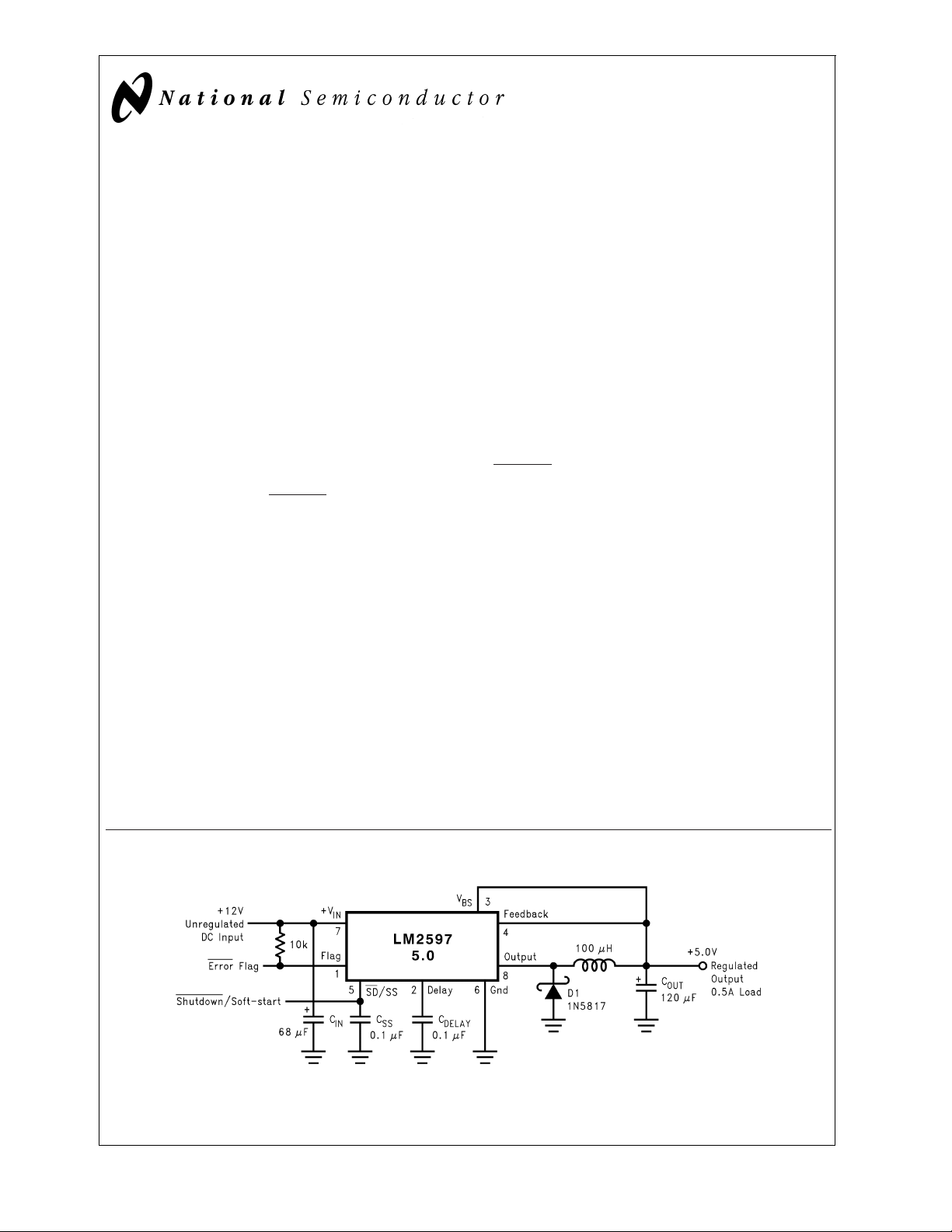
Typical Application (Fixed Output Voltage Versions)
DS012440-1
†
Patent Number 5,382,918.
SIMPLE SWITCHER®and
© 2001 National Semiconductor Corporation DS012440 www.national.com
Switchers Made Simple
®
are registered trademarks of National Semiconductor Corporation.

Absolute Maximum Ratings (Note 1)
If Military/Aerospace specified devices are required,
please contact the National Semiconductor Sales Office/
Distributors for availability and specifications.
Maximum Supply Voltage (V
LM2597 45V
LM2597/LM2597HV
LM2597HV 60V
SD /SS Pin Input Voltage (Note 2)
)
IN
6V
ESD Susceptibility
Human Body Model (Note 3) 2 kV
Lead Temperature
M8 Package
Vapor Phase (60 sec.) +215˚C
Infrared (15 sec.) +220˚C
N Package (Soldering, 10 sec.) +260˚C
Maximum Junction Temperature +150˚C
Delay Pin Voltage (Note 2) 1.5V
Flag Pin Voltage −0.3 ≤ V ≤45V
Bias Supply Voltage (V
) −0.3 ≤ V ≤30V
BS
Feedback Pin Voltage −0.3 ≤ V ≤+25V
Output Voltage to Ground
(Steady State) −1V
Power Dissipation Internally limited
Operating Conditions
Temperature Range −40˚C ≤ TJ+125˚C
Supply Voltage
LM2597 4.5V to 40V
LM2597HV 4.5V to 60V
Storage Temperature Range −65˚C to +150˚C
LM2597/LM2597HV-3.3
Electrical Characteristics
Specifications with standard type face are for TJ= 25˚C, and those with boldface type apply over full Operating Temperature Range.V
Symbol Parameter Conditions LM2597/LM2597HV-3.3 Units
SYSTEM PARAMETERS (Note 6) Test Circuit
V
OUT
Output Voltage 4.75V ≤ VIN≤ V
η Efficiency V
=40V for the LM2597 and 60V for the LM2597HV
INmax
Figure 12
, 0.1A ≤ I
INmax
= 12V, I
IN
= 0.5A 80 %
LOAD
Typ Limit
(Note 4) (Note 5)
≤ 0.5A 3.3 V
LOAD
3.168/3.135 V(min)
3.432/3.465 V(max)
(Limits)
LM2597/LM2597HV-5.0
Electrical Characteristics
Specifications with standard type face are for TJ= 25˚C, and those with boldface type apply over full Operating Temperature Range.V
Symbol Parameter Conditions LM2597/LM2597HV-5.0 Units
SYSTEM PARAMETERS (Note 6) Test Circuit
V
OUT
Output Voltage 7V ≤ VIN≤ V
η Efficiency V
=40V for the LM2597 and 60V for the LM2597HV
INmax
Figure 12
, 0.1A ≤ I
INmax
= 12V, I
IN
= 0.5A 82 %
LOAD
Typ Limit
(Note 4) (Note 5)
≤ 0.5A 5 V
LOAD
4.800/4.750 V(min)
5.200/5.250 V(max)
(Limits)
www.national.com 2
LM2597/LM2597HV-12
Electrical Characteristics
Specifications with standard type face are for TJ= 25˚C, and those with boldface type apply over full Operating Temperature Range.V
=40V for the LM2597 and 60V for the LM2597HV
INmax
Symbol Parameter Conditions LM2597/LM2597HV-12 Units
Typ Limit
(Limits)
(Note 4) (Note 5)
SYSTEM PARAMETERS (Note 6) Test Circuit
V
OUT
Output Voltage 15V ≤ VIN≤ V
Figure 12
, 0.1A ≤ I
INmax
≤ 0.5A 12 V
LOAD
11.52/11.40 V(min)
12.48/12.60 V(max)
η Efficiency V
= 25V, I
IN
= 0.5A 88 %
LOAD
LM2597/LM2597HV-ADJ
Electrical Characteristics
Specifications with standard type face are for TJ= 25˚C, and those with boldface type apply over full Operating Temperature Range.V
Symbol Parameter Conditions LM2597/LM2597HV-ADJ Units
SYSTEM PARAMETERS (Note 6) Test Circuit
V
FB
Feedback Voltage 4.5V ≤ VIN≤ V
η Efficiency V
=40V for the LM2597 and 60V for the LM2597HV
INmax
Figure 12
, 0.1A ≤ I
INmax
V
programmed for 3V. Circuit of
OUT
= 12V, V
IN
OUT
= 3V, I
Typ Limit
(Note 4) (Note 5)
≤ 0.5A 1.230 V
LOAD
Figure 12
. 1.193/1.180 V(min)
1.267/1.280 V(max)
= 0.5A 80 %
LOAD
(Limits)
LM2597/LM2597HV
All Output Voltage Versions
Electrical Characteristics
Specifications with standard type face are for TJ= 25˚C, and those with boldface type apply over full Operating Temperature Range. Unless otherwise specified, V
sion. I
LOAD
= 100 mA.
Symbol Parameter Conditions LM2597/LM2597HV-XX Units
DEVICE PARAMETERS
I
b
f
O
V
SAT
Feedback Bias Current Adjustable Version Only, VFB= 1.235V 10 50/100 nA
Oscillator Frequency (Note 7) 150 kHz
Saturation Voltage I
DC Max Duty Cycle (ON) (Note 9) 100 %
Min Duty Cycle (OFF) (Note 10) 0
I
CL
I
L
I
Q
Current Limit Peak Current, (Notes 8 and 9) 0.8 A
Output Leakage Current (Notes 8, 10 and 11) Output = 0V 50 µA(max)
Operating Quiescent SD /SS Pin Open, VBSPin Open(Note 10) 5mA
= 12V for the 3.3V, 5V, and Adjustable version and VIN= 24V for the 12V ver-
IN
Typ Limit
(Limits)
(Note 4) (Note 5)
127/110 kHz(min)
173/173 kHz(max)
= 0.5A (Notes 8 and 9) 0.9 V
OUT
1.1/1.2 V(max)
0.65/0.58 A(min)
1.3/1.4 A(max)
Output = −1V 2 mA
15 mA(max)
www.national.com3
All Output Voltage Versions
Electrical Characteristics
Specifications with standard type face are for TJ= 25˚C, and those with boldface type apply over full Operating Temperature Range. Unless otherwise specified, V
sion. I
Symbol Parameter Conditions LM2597/LM2597HV-XX Units
LM2597/LM2597HV
DEVICE PARAMETERS
I
STBY
θ
JA
SHUTDOWN/SOFT-START CONTROL Test Circuit of
V
SD
V
SS
I
SD
I
SS
FLAG/DELAY CONTROL Test Circuit of
VF
SAT
IF
L
BIAS SUPPLY
I
BS
I
Q
Note 1: Absolute Maximum Ratings indicate limits beyond which damage to the device may occur. Operating Ratings indicate conditions for which the device is
intended to be functional, but do not guarantee specific performance limits. For guaranteed specifications and test conditions, see the Electrical Characteristics.
Note 2: Voltage internally clamped. If clamp voltage is exceeded, limit current to a maximum of 1 mA.
Note 3: The human body model is a 100 pF capacitor discharged through a 1.5k resistor into each pin.
Note 4: Typical numbers are at 25˚C and represent the most likely norm.
= 100 mA.
LOAD
Current 10 mA(max)
Standby Quiescent SD /SS pin = 0V (Note 10)LM2597 85 µA
Current 200/250 µA(max)
Thermal Resistance N Package, Junction to Ambient (Note 12) 95 ˚C/W
Shutdown Threshold 1.3 V
Voltage Low, (Shutdown Mode) 0.6 V(max)
Soft-start Voltage V
Shutdown Current V
Soft-start Current V
Regulator Dropout Low (Flag ON) 96 %
Detector 92 %(min)
Threshold Voltage 98 %(max)
Flag Output Saturation I
Voltage V
Flag Output Leakage
Current
Delay Pin Threshold 1.25 V
Voltage Low (Flag ON) 1.21 V(min)
Delay Pin Source V
Current 6 µA(max)
Delay Pin Saturation Low (Flag ON) 55 mV
Bias Supply Pin Current VBS= 2V (Note 10) 120 µA
Operating Quiescent
Current
(Continued)
= 12V for the 3.3V, 5V, and Adjustable version and VIN= 24V for the 12V ver-
IN
Typ Limit
(Note 4) (Note 5)
LM2597HV 140 250/300 µA(max)
M Package, Junction to Ambient (Note 12) 150
Figure 12
High, (Soft-start Mode) 2 V(min)
= 20% of Nominal Output Voltage 2 V
OUT
V
= 100% of Nominal Output Voltage 3
OUT
SHUTDOWN
= 0.5V 5µA
10 µA(max)
= 2.5V 1.6 µA
Soft-start
5 µA(max)
Figure 12
= 3 mA 0.3 V
SINK
= 0.5V 0.7/1.0 V(max)
DELAY
V
= 40V 0.3 µA
FLAG
High (Flag OFF) and V
= 0.5V 3 µA
DELAY
Regulated 1.29 V(max)
OUT
350/400 mV(max)
400 µA(max)
V
= 4.4V (Note 10) 4 mA
BS
10 mA(max)
VBS= 4.4V , Vinpin current(Note 10) 1 2 mA
(Limits)
www.national.com 4
All Output Voltage Versions
Electrical Characteristics
Note 5: All limits guaranteed at room temperature (standard type face) and at temperature extremes (bold type face). All room temperature limits are 100%
production tested. All limits at temperature extremes are guaranteed via correlation using standard Statistical Quality Control (SQC) methods. All limits are used to
calculate Average Outgoing Quality Level (AOQL).
Note 6: External components such as the catch diode, inductor, input and output capacitors can affect switching regulator system performance. When the
LM2597/LM2597HV is used as shown in the
Note 7: The switching frequency is reduced when the second stage current limit is activated. The amount of reduction is determined by the severity of current
overload.
Note 8: No diode, inductor or capacitor connected to output pin.
Note 9: Feedback pin removed from output and connected to 0V to force the output transistor switch ON.
Note 10: Feedback pin removed from output and connected to 12V for the 3.3V,5V,and the ADJ. version, and 15V for the 12V version, to force the output transistor
switch OFF.
Note 11: V
Note 12: Junction to ambient thermal resistance with approximately 1 square inch of printed circuit board copper surrounding the leads. Additional copper area will
lower thermal resistance further. See application hints in this data sheet and the thermal model in Switchers Made Simple
= 40V for the LM2597 and 60V for the LM2597HV.
IN
Figure 12
(Continued)
test circuit, system performance will be as shown in system parameters section of Electrical Characteristics.
™
software.
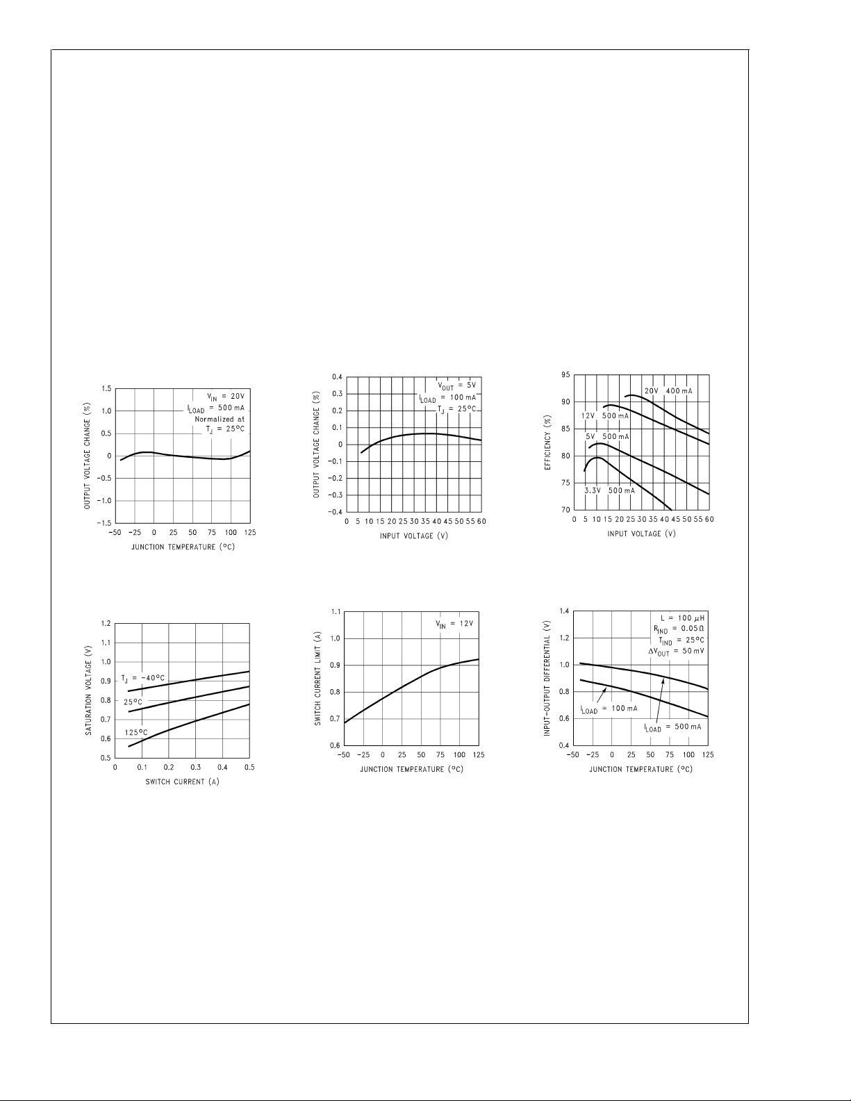
Typical Performance Characteristics
LM2597/LM2597HV
Normalized
Output Voltage
Switch Saturation
Voltage
DS012440-2
Line Regulation
Switch Current Limit
DS012440-3
Efficiency
DS012440-4
Dropout Voltage
DS012440-5
DS012440-6
DS012440-7
www.national.com5
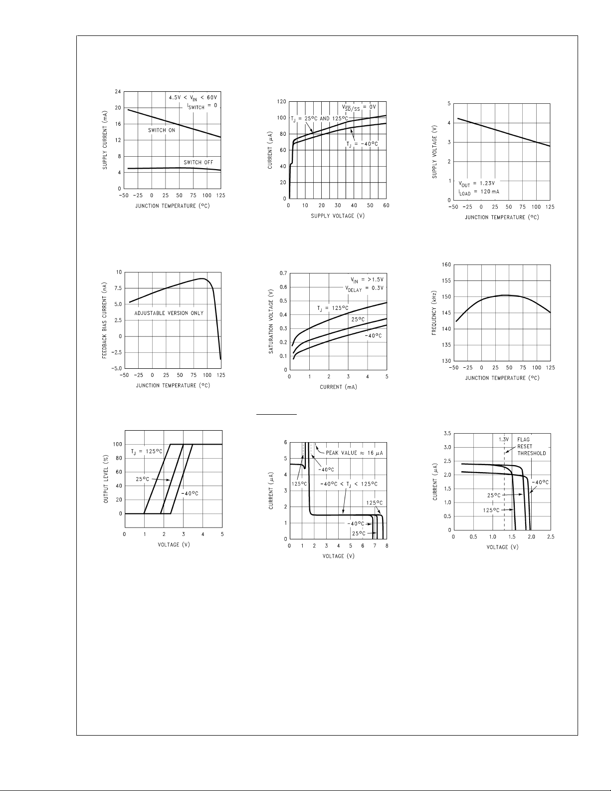
Typical Performance Characteristics (Continued)
Quiescent Current
LM2597/LM2597HV
Feedback Pin
Bias Current
DS012440-8
Standby
Quiescent Current
Flag Saturation
Voltage
DS012440-9
Minimum Operating
Supply Voltage
DS012440-10
Switching Frequency
Soft-start
DS012440-11
DS012440-14
Shutdown /Soft-start
Current
DS012440-12
DS012440-13
Delay Pin Current
DS012440-16
DS012440-15
www.national.com 6
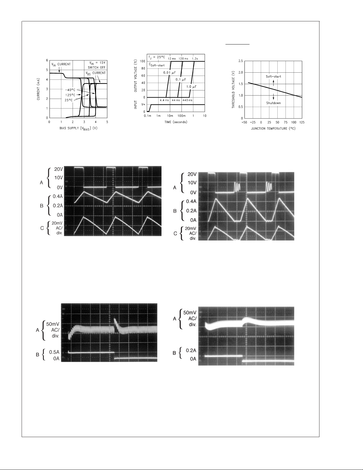
Typical Performance Characteristics (Continued)
V
and VBSCurrent vs
IN
V
and Temperature
BS
DS012440-17
Soft-start Response
DS012440-18
LM2597/LM2597HV
Shutdown /Soft-start
Threshold Voltage
DS012440-25
Continuous Mode Switching Waveforms
V
= 20V, V
IN
L = 100 µH, C
A: Output Pin Voltage, 10V/div.
B: Inductor Current 0.2A/div.
C: Output Ripple Voltage, 20 mV/div.
OUT
OUT
=5V,I
LOAD
= 120 µF, C
= 400 mA
ESR = 140 mΩ
OUT
Horizontal Time Base: 2 µs/div.
Load Transient Response for Continuous Mode
V
= 20V, V
IN
L = 100 µH, C
OUT
OUT
=5V,I
LOAD
= 120 µF, C
= 200 mA to 500 mA
ESR = 140 mΩ
OUT
DS012440-19
Discontinuous Mode Switching Waveforms
= 20V, V
V
IN
L = 33 µH, C
A: Output Pin Voltage, 10V/div.
B: Inductor Current 0.2A/div.
C: Output Ripple Voltage, 20 mV/div.
OUT
OUT
=5V,I
LOAD
= 220 µF, C
= 200 mA
ESR=60mΩ
OUT
DS012440-20
Horizontal Time Base: 2 µs/div.
Load Transient Response for Discontinuous Mode
= 20V, V
V
IN
L = 33 µH, C
OUT
OUT
=5V,I
LOAD
= 220 µF, C
= 100 mA to 200 mA
ESR=60mΩ
OUT
A: Output Voltage, 50 mV/div. (AC)
B: 200 mA to 500 mA Load Pulse
Horizontal Time Base: 50 µs/div.
DS012440-21
DS012440-22
A: Output Voltage, 50 mV/div. (AC)
B: 100 mA to 200 mA Load Pulse
Horizontal Time Base: 200 µs/div.
www.national.com7
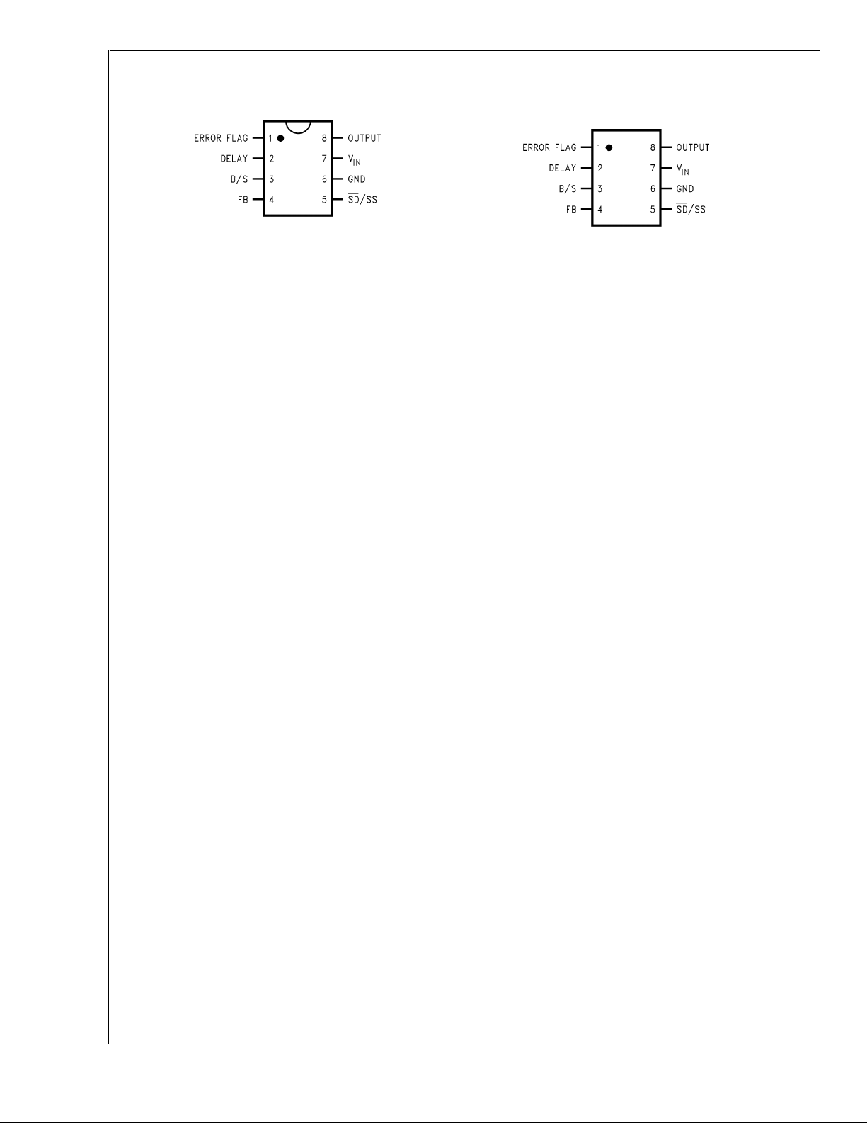
Connection Diagrams and Ordering Information
LM2597/LM2597HV
Order Number LM2597N-3.3,
LM2597N-5.0, LM2597N-12 or
LM2597HVN-3.3, LM2597HVN-5.0,
LM2597HVN-12 or LM2597HVN-ADJ
See NS Package Number N08E
8–Lead DIP (N)
Top View
LM2597N-ADJ
DS012440-23
8–Lead Surface Mount (M)
DS012440-24
Top View
Order Number LM2597M-3.3,
LM2597M-5.0, LM2597M-12 or
LM2597M-ADJ
LM2597HVM-3.3, LM2597HVM-5.0,
LM2597HVM-12 or LM2597HVM-ADJ
See NS Package Number M08A
www.national.com 8
LM2597/LM2597HV Series Buck Regulator Design Procedure (Fixed
Output)
PROCEDURE (Fixed Output Voltage Version) EXAMPLE (Fixed Output Voltage Version)
Given:
V
= Regulated Output Voltage (3.3V, 5V or 12V)
OUT
V
(max) = Maximum DC Input Voltage
IN
I
(max) = Maximum Load Current
LOAD
1. Inductor Selection (L1)
A. Select the correct inductor value selection guide from
Figure 3,Figure 4
,or
Figure 5
. (Output voltages of 3.3V,5V,or
12V respectively.) For all other voltages, see the design procedure for the adjustable version.
B. From the inductor value selection guide, identify the inductance region intersected by the Maximum Input Voltage line
and the Maximum Load Current line. Each region is identified
by an inductance value and an inductor code (LXX).
C. Select an appropriate inductor from the four manufacturer’s
part numbers listed in
2. Output Capacitor Selection (C
Figure 7
.
)
OUT
A. In the majority of applications, low ESR (Equivalent Series
Resistance) electrolytic capacitors between 82 µF and 220 µF
and low ESR solid tantalum capacitors between 15 µF and
100 µF provide the best results. This capacitor should be
located close to the IC using short capacitor leads and short
copper traces. Do not use capacitors larger than 220 µF.
For additional information, see section on output capacitors in application information section.
B. To simplify the capacitor selection procedure, refer to the
quick design component selection table shown in
Figure 1
This table contains different input voltages, output voltages,
and load currents, and lists various inductors and output
capacitors that will provide the best design solutions.
C. The capacitor voltage rating for electrolytic capacitors
should be at least 1.5 times greater than the output voltage,
and often much higher voltage ratings are needed to satisfy
the low ESR requirements for low output ripple voltage.
D. For computer aided design software, see
®
Simple
version 4.1 or later).
Switchers Made
Given:
=5V
V
OUT
V
(max) = 12V
IN
I
(max) = 0.4A
LOAD
1. Inductor Selection (L1)
A. Use the inductor selection guide for the 5V version shown
Figure 4
in
.
B. From the inductor value selection guide shown in
the inductance region intersected by the 12V horizontal line
and the 0.4A vertical line is 100 µH, and the inductor code is
L20.
C. The inductance value required is 100 µH. From the table in
Figure 7
, go to the L20 line and choose an inductor part
number from any of the four manufacturers shown. (In most
instance, both through hole and surface mount inductors are
available.)
2. Output Capacitor Selection (C
OUT
)
A. See section on output capacitors in application information section.
B. From the quick design component selection table shown in
Figure 1
, locate the 5V output voltage section. In the load
current column, choose the load current line that is closest to
the current needed in your application, for this example, use
the 0.5Aline. In the maximum input voltage column, select the
line that covers the input voltage needed in your application,
in this example, use the 15V line. Continuing on this line are
recommended inductors and capacitors that will provide the
.
best overall performance.
The capacitor list contains both through hole electrolytic and
surface mount tantalum capacitors from four different capacitor manufacturers. It is recommended that both the manufacturers and the manufacturer’s series that are listed in the table
be used.
In this example aluminum electrolytic capacitors from several
different manufacturers are available with the range of ESR
numbers needed.
120 µF 25V Panasonic HFQ Series
120 µF 25V Nichicon PL Series
C. For a 5V output, a capacitor voltage rating at least 7.5V or
more is needed. But, in this example, even a low ESR,
switching grade, 120 µF 10V aluminum electrolytic capacitor
would exhibit approximately 400 mΩ of ESR (see the curve in
Figure 17
for the ESR vs voltage rating). This amount of ESR
would result in relatively high output ripple voltage. To reduce
the ripple to 1% of the output voltage, or less, a capacitor with
a higher voltage rating (lower ESR) should be selected. A 16V
or 25V capacitor will reduce the ripple voltage by approximately half.
Figure 4
LM2597/LM2597HV
,
www.national.com9
LM2597/LM2597HV Series Buck Regulator Design Procedure (Fixed
Output)
3. Catch Diode Selection (D1)
A. The catch diode current rating must be at least 1.3 times
LM2597/LM2597HV
greater than the maximum load current. Also, if the power
supply design must withstand a continuous output short, the
diode should have a current rating equal to the maximum
current limit of the LM2597. The most stressful condition for
this diode is an overload or shorted output condition.
B. The reverse voltage rating of the diode should be at least
1.25 times the maximum input voltage.
C. This diode must be fast (short reverse recovery time) and
must be located close to the LM2597 using short leads and
short printed circuit traces. Because of their fast switching
speed and low forward voltage drop, Schottky diodes provide
the best performance and efficiency, and should be the first
choice, especially in low output voltage applications. Ultra-fast
recovery, or High-Efficiency rectifiers also provide good results. Ultra-fast recovery diodes typically have reverse recovery times of 50 ns or less. Rectifiers such as the 1N4001
series are much too slow and should not be used.
4. Input Capacitor (C
A low ESR aluminum or tantalum bypass capacitor is needed
between the input pin and ground to prevent large voltage
transients from appearing at the input. In addition, the RMS
current rating of the input capacitor should be selected to be
at least
data sheet must be checked to assure that this current rating
is not exceeded. The curve shown in
RMS current ratings for several different aluminum electrolytic
capacitor values.
This capacitor should be located close to the IC using short
leads and the voltage rating should be approximately 1.5
times the maximum input voltage.
If solid tantalum input capacitors are used, it is recommended
that they be surge current tested by the manufacturer.
Use caution when using ceramic capacitors for input bypassing, because it may cause severe ringing at the V
For additional information, see section on input capacitors in Application Information section.
(Continued)
PROCEDURE (Fixed Output Voltage Version) EXAMPLE (Fixed Output Voltage Version)
3. Catch Diode Selection (D1)
A. Refer to the table shown in
Figure 10
1A, 20V, 1N5817 Schottky diode will provide the best performance, and will not be overstressed even for a shorted output.
)
IN
4. Input Capacitor (C
)
IN
The important parameters for the Input capacitor are the input
voltage rating and the RMS current rating. With a nominal
input voltage of 12V, an aluminum electrolytic capacitor with a
1
⁄2the DC load current. The capacitor manufacturers
Figure 16
shows typical
voltage rating greater than 18V (1.5 x V
The next higher capacitor voltage rating is 25V.
The RMS current rating requirement for the input capacitor in
a buck regulator is approximately
this example, with a 400 mA load, a capacitor with a RMS
current rating of at least 200 mAis needed. The curves shown
in
Figure 16
can be used to select an appropriate input
capacitor.From the curves, locate the 25Vline and note which
capacitor values have RMS current ratings greater than 200
mA. Either a 47 µF or 68 µF, 25V capacitor could be used.
For a through hole design, a 68 µF/25V electrolytic capacitor
(Panasonic HFQ series or Nichicon PL series or equivalent)
pin.
IN
would be adequate. Other types or other manufacturers capacitors can be used provided the RMS ripple current ratings
are adequate.
For surface mount designs, solid tantalum capacitors are
recommended. The TPS series available from AVX, and the
593D series from Sprague are both surge current tested.
. In this example, a
) would be needed.
IN
1
⁄2the DC load current. In
www.national.com 10
LM2597/LM2597HV Series Buck Regulator Design Procedure (Fixed
Output)
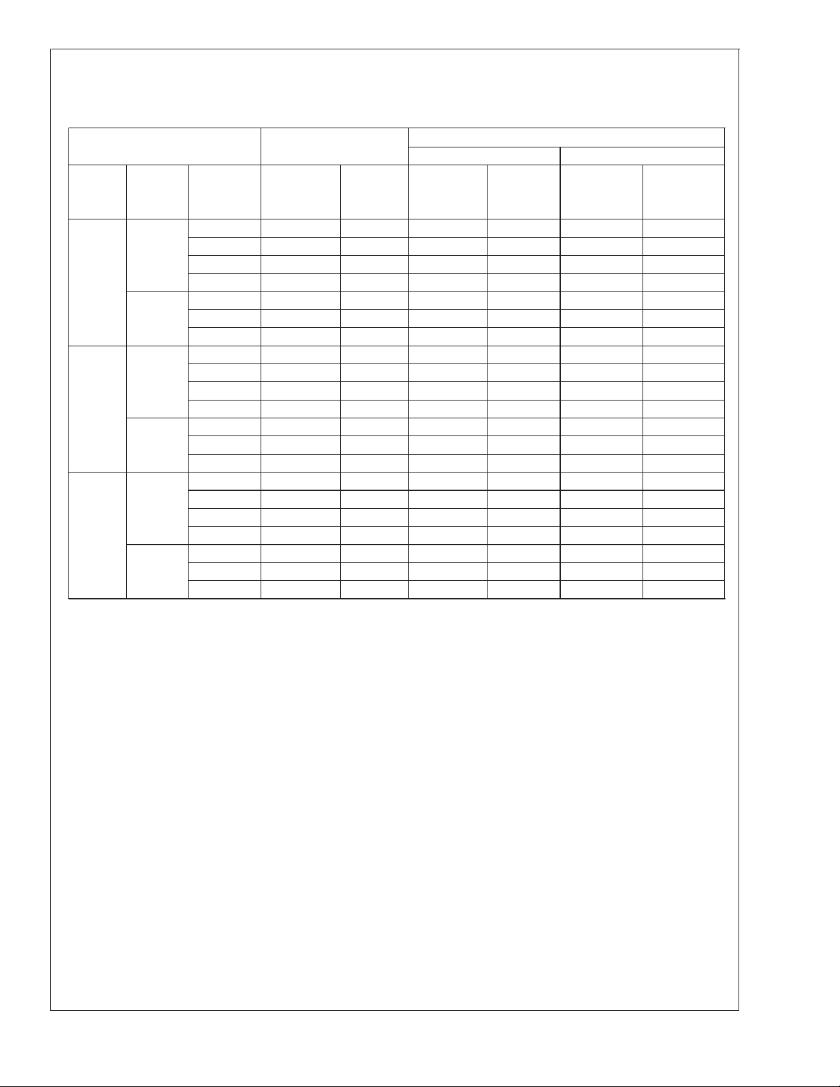
Output Load Max Input Inductance Inductor Panasonic Nichicon AVX TPS Sprague
Voltage Current Voltage (µH) (
(V) (A) (V) (µF/V) (µF/V) (µF/V) (µF/V)
3.3 0.5 5 33 L14 220/16 220/16 100/16 100/6.3
5 0.5 8 47 L13 180/16 180/16 100/16 33/25
12 0.5 15 68 L21 82/25 82/25 100/16 15/25
(Continued)
Conditions Inductor Output Capacitor
Through Hole Surface Mount
#
) HFQ Series PL Series Series 595D Series
7 47 L13 120/25 120/25 100/16 100/6.3
10 68 L21 120/25 120/25 100/16 100/6.3
40 100 L20 120/35 120/35 100/16 100/6.3
6 68 L4 120/25 120/25 100/16 100/6.3
0.2 10 150 L10 120/16 120/16 100/16 100/6.3
40 220 L9 120/16 120/16 100/16 100/6.3
10 68 L21 180/16 180/16 100/16 33/25
15 100 L20 120/25 120/25 100/16 33/25
40 150 L19 120/25 120/25 100/16 33/25
9 150 L10 82/16 82/16 100/16 33/25
0.2 20 220 L9 120/16 120/16 100/16 33/25
40 330 L8 120/16 120/16 100/16 33/25
18 150 L19 82/25 82/25 100/16 15/25
30 220 L27 82/25 82/25 100/16 15/25
40 330 L26 82/25 82/25 100/16 15/25
15 100 L11 82/25 82/25 100/16 15/25
0.2 20 220 L9 82/25 82/25 100/16 15/25
40 330 L17 82/25 82/25 100/16 15/25
LM2597/LM2597HV
FIGURE 1. LM2597/LM2597HV Fixed Voltage Quick Design Component Selection Table
www.national.com11
 Loading...