

National Semiconductor LM2593HV Technical data

LM2593HV
SIMPLE SWITCHER
®
Power Converter 150 kHz 2A
Step-Down Voltage Regulator, with Features
December 2001
LM2593HV SIMPLE SWITCHER Power Converter 150 kHz 2A Step-Down Voltage Regulator, with
Features
General Description
The LM2593HV series of regulators are monolithic integrated circuits that provide all the active functions for a
step-down (buck) switching regulator, capable of driving a
2A load with excellent line and load regulation. These devices are available in fixed output voltages of 3.3V, 5V, and
an adjustable output version.
This series of switching regulators is similar to the
LM2592HV withadditionalsupervisory and performance features.
Requiring a minimum number of external components, these
regulators are simple to use and include internal frequency
compensation
fixed-frequency oscillator, Shutdown/Soft-start, output error
flag and flag delay.
The LM2593HV operates at a switching frequency of 150
kHz thus allowing smaller sized filter components than what
would be needed with lower frequency switching regulators.
Available in a standard 7-lead TO-220 package with several
different lead bend options, and a 7-lead TO-263 Surface
mount package.
Other features include a guaranteed
put voltage under all conditions of input voltage and output
load conditions, and
ternal shutdown is included, featuring typically 90 µA
standby current. Self protection features include a two stage
current limit for the output switch and an over temperature
shutdown for complete protection under fault conditions.
†
, improved line and load specifications,
±
4% tolerance on out-
±
15% on the oscillator frequency. Ex-
Features
n 3.3V, 5V, and adjustable output versions
n Adjustable version output voltage range, 1.2V to 57V
±
4% max over line and load conditions
n Guaranteed 2A output load current
n Available in 7-pin TO-220 and TO-263 (surface mount)
Package
n Input voltage range up to 60V
n 150 kHz fixed frequency internal oscillator
n Shutdown/Soft-start
n Out of regulation error flag
n Error flag delay
n Low power standby mode, I
n High Efficiency
n Thermal shutdown and current limit protection
typically 90 µA
Q
Applications
n Simple high-efficiency step-down (buck) regulator
n Efficient pre-regulator for linear regulators
n On-card switching regulators
n Positive to Negative converter
Note:†Patent Number 5,382,918.
Typical Application (Fixed Output Voltage Versions)
10133301
SIMPLE SWITCHER®and
© 2001 National Semiconductor Corporation DS101333 www.national.com
Switchers Made Simple
®
are registered trademarks of National Semiconductor Corporation.
Absolute Maximum Ratings (Note 1)
If Military/Aerospace specified devices are required,
please contact the National Semiconductor Sales Office/
LM2593HV
Distributors for availability and specifications.
Maximum Supply Voltage (V
SD /SS Pin Input Voltage (Note 2)
Delay Pin Voltage (Note 2) 1.5V
Flag Pin Voltage −0.3 ≤ V ≤45V
Feedback Pin Voltage −0.3 ≤ V ≤+25V
Output Voltage to Ground
(Steady State) −1V
Power Dissipation Internally limited
Storage Temperature Range −65˚C to +150˚C
) 63V
IN
6V
ESD Susceptibility
Human Body Model (Note 3) 2 kV
Lead Temperature
S Package
Vapor Phase (60 sec.) +215˚C
Infrared (10 sec.) +245˚C
T Package (Soldering, 10 sec.) +260˚C
Maximum Junction Temperature +150˚C
Operating Conditions
Temperature Range −40˚C ≤ TJ≤ +125˚C
Supply Voltage 4.5V to 60V
LM2593HV-3.3 Electrical Characteristics
Specifications with standard type face are for TJ= 25˚C, and those with boldface type apply over full Operating Temperature Range.
Symbol Parameter Conditions LM2593HV-3.3 Units
Typ Limit
(Note 4) (Note 5)
SYSTEM PARAMETERS (Note 6) Test Circuit
V
OUT
η Efficiency V
Output Voltage 4.75V ≤ VIN≤ 60V, 0.2A ≤ I
= 12V, I
IN
Figure 1
≤ 2A 3.3 V
LOAD
=2A 76
LOAD
3.168/3.135 V(min)
3.432/3.465 V(max)
(Limits)
LM2593HV-5.0 Electrical Characteristics
Specifications with standard type face are for TJ= 25˚C, and those with boldface type apply over full Operating Temperature Range.
Symbol Parameter Conditions LM2593HV-5.0 Units
(Limits)
SYSTEM PARAMETERS (Note 6) Test Circuit
V
OUT
η Efficiency V
Output Voltage 7V ≤ VIN≤ 60V, 0.2A ≤ I
= 12V, I
IN
Typ Limit
(Note 4) (Note 5)
Figure 1
≤ 2A 5 V
LOAD
4.800/4.750 V(min)
5.200/5.250 V(max)
=2A 81 %
LOAD
LM2593HV-ADJ Electrical Characteristics
Specifications with standard type face are for TJ= 25˚C, and those with boldface type apply over full Operating Temperature Range.
Symbol Parameter Conditions LM2593HV-ADJ Units
(Limits)
SYSTEM PARAMETERS (Note 6) Test Circuit
V
FB
Feedback Voltage 4.5V ≤ VIN≤ 60V, 0.2A ≤ I
V
programmed for 3V. Circuit of
OUT
Figure 1
Typ Limit
(Note 4) (Note 5)
≤ 2A 1.230 V
LOAD
Figure 1
. 1.193/1.180 V(min)
1.267/1.280 V(max)
www.national.com 2
LM2593HV-ADJ
Electrical Characteristics
Specifications with standard type face are for TJ= 25˚C, and those with boldface type apply over full Operating Temperature Range.
Symbol Parameter Conditions LM2593HV-ADJ Units
η Efficiency V
= 12V, V
IN
(Continued)
= 3V, I
OUT
Typ Limit
(Note 4) (Note 5)
=2A 75 %
LOAD
(Limits)
All Output Voltage Versions Electrical Characteristics
Specifications with standard type face are for TJ= 25˚C, and those with boldface type apply over full Operating Temperature Range. Unless otherwise specified, V
Symbol Parameter Conditions LM2593HV-XX Units
DEVICE PARAMETERS
I
b
f
O
V
SAT
Feedback Bias Current Adjustable Version Only, VFB= 1.3V 10 nA
Oscillator Frequency (Note 7) 150 kHz
Saturation Voltage I
DC Max Duty Cycle (ON) (Note 9) 100 %
Min Duty Cycle (OFF) (Note 10) 0
I
I
I
CLIM
L
Q
Switch current Limit Peak Current, (Note 8) (Note 9) 3.0 A
Output Leakage Current (Note 8) (Note 10) (Note 11) Output = 0V 50 µA(max)
Operating Quiescent SD /SS Pin Open (Note 10) 5mA
Current 10 mA(max)
I
STBY
Standby Quiescent SD /SS pin = 0V (Note 11) 90 µA
Current 200/250 µA(max)
θ
JC
θ
JA
θ
JA
θ
JA
θ
JA
Thermal Resistance TO220 or TO263 Package, Junction to Case 2 ˚C/W
SHUTDOWN/SOFT-START CONTROL Test Circuit of
V
SD
Shutdown Threshold 1.3 V
Voltage Low, (Shutdown Mode) 0.6 V(max)
V
SS
I
SD
I
SS
Soft-start Voltage V
Shutdown Current V
Soft-start Current V
= 12V for the 3.3V, 5V, and Adjustable version. I
IN
= 500 mA
LOAD
Typ Limit
(Limits)
(Note 4) (Note 5)
50/100 nA (max)
127/110 kHz(min)
173/173 kHz(max)
= 2A (Note 8) (Note 9) 1.10 V
OUT
1.3/1.4 V(max)
2.4/2.3 A(min)
3.7/4.0 A(max)
Output = −1V 5 mA
30 mA(max)
TO220 Package, Juncton to Ambient (Note 12) 50 ˚C/W
TO263 Package, Juncton to Ambient (Note 13) 50 ˚C/W
TO263 Package, Juncton to Ambient (Note 14) 30 ˚C/W
TO263 Package, Juncton to Ambient (Note 15) 20 ˚C/W
Figure 1
High, (Soft-start Mode) 2 V(min)
= 20% of Nominal Output Voltage 2 V
OUT
V
= 100% of Nominal Output Voltage 3
OUT
SHUTDOWN
= 0.5V 5µA
10 µA(max)
Soft-start
= 2.5V 1.5 µA
5 µA(max)
LM2593HV
www.national.com3
All Output Voltage Versions
Electrical Characteristics
Specifications with standard type face are for TJ= 25˚C, and those with boldface type apply over full Operating Tempera-
LM2593HV
ture Range. Unless otherwise specified, V
Symbol Parameter Conditions LM2593HV-XX Units
FLAG/DELAY CONTROL Test Circuit of
Regulator Dropout Detector Low (Flag ON) 96 %
Threshold Voltage 92 %(min)
VF
SAT
IF
L
Note 1: Absolute Maximum Ratings indicate limits beyond which damage to the device may occur. Operating Ratings indicate conditions for which the device is
intended to be functional, but do not guarantee specific performance limits. For guaranteed specifications and test conditions, see the Electrical Characteristics.
Note 2: Voltage internally clamped. If clamp voltage is exceeded, limit current to a maximum of 1 mA.
Note 3: The human body model is a 100 pF capacitor discharged through a 1.5k resistor into each pin.
Note 4: Typical numbers are at 25˚C and represent the most likely norm.
Note 5: All limits guaranteed at room temperature (standard type face) and at temperature extremes (bold type face). All room temperature limits are 100%
production tested. All limits at temperature extremes are guaranteed via correlation using standard Statistical Quality Control (SQC) methods. All limits are used
to calculate Average Outgoing Quality Level (AOQL).
Note 6: External components such as the catch diode, inductor, input and output capacitors can affect switching regulator system performance. When the
LM2593HV is used as shown in the
Note 7: The switching frequency is reduced when the second stage current limit is activated. The amount of reduction is determined by the severity of current
overload.
Note 8: No diode, inductor or capacitor connected to output pin.
Note 9: Feedback pin removed from output and connected to 0V to force the output transistor switch ON.
Note 10: Feedback pin removed from output and connected to 12V for the 3.3V, 5V, and the ADJ. version to force the output transistor switch OFF.
Note 11: V
Note 12: Junction to ambient thermal resistance (no external heat sink) for the package mounted TO-220 package mounted vertically, with the leads soldered to
a printed circuit board with (1 oz.) copper area of approximately 1 in
Note 13: Junction to ambient thermal resistance with the TO-263 package tab soldered to a single sided printed circuit board with 0.5 in
Note 14: Junction to ambient thermal resistance with the TO-263 package tab soldered to a single sided printed circuit board with 2.5 in
Note 15: Junction to ambient thermal resistance with the TO-263 package tab soldered to a double sided printed circuit board with 3 in
the LM2593HVS side of the board, and approximately 16 in
model in Switchers Made Simple available at http://power.national.com.
Flag Output Saturation I
Voltage V
Flag Output Leakage Current V
Delay Pin Threshold 1.25 V
Voltage Low (Flag ON) 1.21 V(min)
Delay Pin Source Current V
Delay Pin Saturation Low (Flag ON) 70 mV
Figure 1
= 60V.
IN
(Continued)
= 12V for the 3.3V, 5V, and Adjustable version. I
IN
LOAD
= 500 mA
Typ Limit
(Note 4) (Note 5)
Figure 1
98 %(max)
= 3 mA 0.3 V
SINK
= 0.5V 0.7/1.0 V(max)
DELAY
= 60V 0.3 µA
FLAG
High (Flag OFF) and V
= 0.5V 3 µA
DELAY
Regulated 1.29 V(max)
OUT
6 µA(max)
350/400 mV(max)
test circuit, system performance will be as shown in system parameters section of Electrical Characteristics.
2
.
2
of copper on the other side of the p-c board. See application hints in this data sheet and the thermal
2
of (1 oz.) copper area.
2
of (1 oz.) copper area.
2
of (1 oz.) copper area on
(Limits)
www.national.com 4
LM2593HV
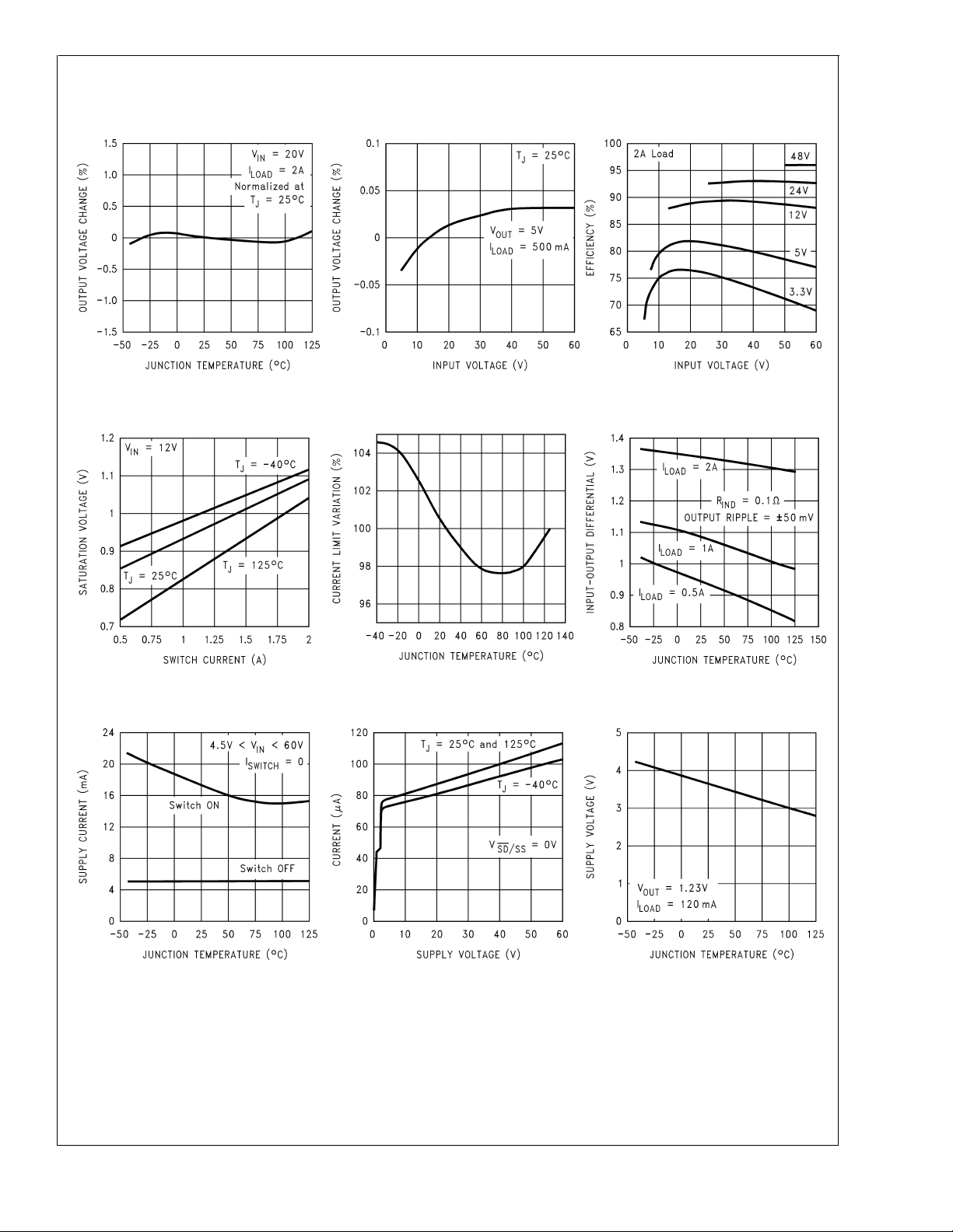
Typical Performance Characteristics (Circuit of
Normalized
Output Voltage Line Regulation Efficiency
10133302
Switch Saturation
Voltage Switch Current Limit Dropout Voltage
Figure 1
)
10133303 10133304
Operating
Quiescent Current
10133305
10133306
Shutdown
Quiescent Current
10133308 10133309
10133307
Minimum Operating
Supply Voltage
10133310
www.national.com5
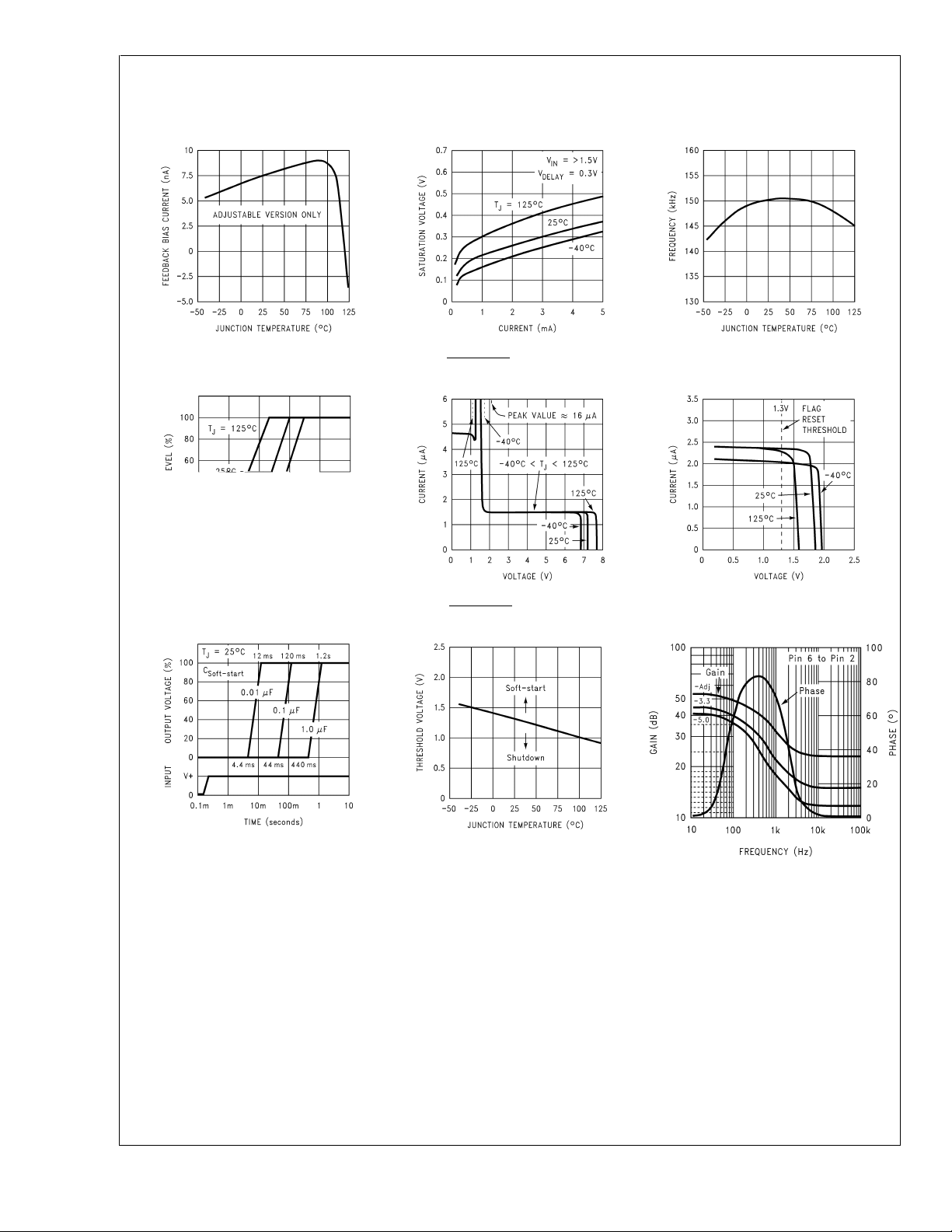
Typical Performance Characteristics (Circuit of
Figure 1
) (Continued)
LM2593HV
Feedback Pin
Bias Current
Soft-start
10133311
Flag Saturation
Voltage Switching Frequency
10133312
Shutdown /Soft-start
Current Delay Pin Current
10133313
Soft-start Response
10133314
10133318
10133315
10133316
Shutdown/Soft-start
Threshold Voltage Internal Gain-Phase Characteristics
10133353
10133378
www.national.com 6
LM2593HV
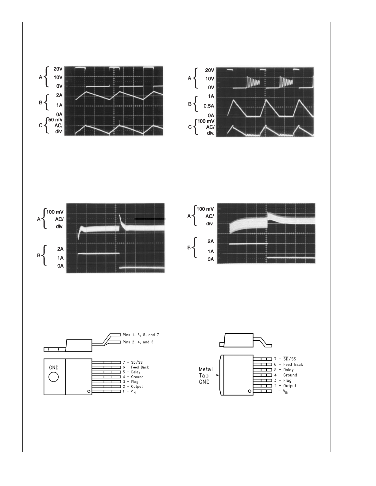
Typical Performance Characteristics (Circuit of
Continuous Mode Switching Waveforms
V
= 20V, V
L = 32 µH, C
IN
OUT
Horizontal Time Base: 2 µs/div.
A: Output Pin Voltage, 10V/div.
B: Inductor Current 1A/div.
C: Output Ripple Voltage, 50 mV/div.
Load Transient Response for Continuous Mode
V
= 20V, V
IN
L = 32 µH, C
OUT
OUT
= 5V, I
OUT
= 220 µF, C
= 5V, I
LOAD
= 220 µF, C
=2A
LOAD
ESR=50mΩ
OUT
= 500 mA to 2A
ESR=50mΩ
OUT
10133320
A: Output Pin Voltage, 10V/div.
B: Inductor Current 0.5A/div.
C: Output Ripple Voltage, 100 mV/div.
Load Transient Response for Discontinuous Mode
Figure 1
) (Continued)
Discontinuous Mode Switching Waveforms
V
= 20V, V
IN
L = 10 µH, C
OUT
= 5V, I
OUT
= 330 µF, C
= 500 mA
LOAD
ESR=45mΩ
OUT
Horizontal Time Base: 2 µs/div.
V
= 20V, V
IN
L = 10 µH, C
= 5V, I
OUT
= 330 µF, C
OUT
= 500 mA to 2A
LOAD
OUT
ESR=45mΩ
10133319
Horizontal Time Base: 50 µs/div.
10133321
A: Output Voltage, 100 mV/div. (AC)
B: 500 mA to 2A Load Pulse
A: Output Voltage, 100 mV/div. (AC)
B: 500 mA to 2A Load Pulse
Connection Diagrams and Order Information
Bent and Staggered Leads, Through Hole Package
7-Lead TO-220 (T)
Order Number LM2593HVT-3.3, LM2593HVT-5.0,
or LM2593HVT-ADJ
See NS Package Number TA07B
10133350
Order Number LM2593HVS-3.3, LM2593HVS-5.0,
Horizontal Time Base: 200 µs/div.
10133322
Surface Mount Package
7-Lead TO-263 (S)
10133323
or LM2593HVS-ADJ
See NS Package Number TS7B
www.national.com7
 Loading...