

National Semiconductor LM1577, LM2577 Technical data
现货库存、技术资料、百科信息、热点资讯,精彩尽在鼎好!
LM1577/LM2577
SIMPLE SWITCHER
®
Step-Up Voltage Regulator
LM1577/LM2577 SIMPLE SWITCHER Step-Up Voltage Regulator
April 2005
General Description
The LM1577/LM2577 are monolithic integrated circuits that
provide all of the power and control functions for step-up
(boost), flyback, and forward converter switching regulators.
The device is available in three different output voltage
versions: 12V, 15V, and adjustable.
Requiring a minimum number of external components, these
regulators are cost effective, and simple to use. Listed in this
data sheet are a family of standard inductors and flyback
transformers designed to work with these switching regulators.
Included on the chip is a 3.0A NPN switch and its associated
protection circuitry, consisting of current and thermal limiting,
and undervoltage lockout. Other features include a 52 kHz
fixed-frequency oscillator that requires no external components, a soft start mode to reduce in-rush current during
start-up, and current mode control for improved rejection of
input voltage and output load transients.
Connection Diagrams
Straight Leads
5-Lead TO-220 (T)
Features
n Requires few external components
n NPN output switches 3.0A, can stand off 65V
n Wide input voltage range: 3.5V to 40V
n Current-mode operation for improved transient
response, line regulation, and current limit
n 52 kHz internal oscillator
n Soft-start function reduces in-rush current during start-up
n Output switch protected by current limit, under-voltage
lockout, and thermal shutdown
Typical Applications
n Simple boost regulator
n Flyback and forward regulators
n Multiple-output regulator
Bent, Staggered Leads
5-Lead TO-220 (T)
Top View
Order Number LM2577T-12, LM2577T-15,
or LM2577T-ADJ
See NS Package Number T05A
SIMPLE SWITCHER®is a registered trademark of National Semiconductor Corporation.
© 2005 National Semiconductor Corporation DS011468 www.national.com
01146804
Top View
Order Number LM2577T-12 Flow LB03, LM2577T-15
Flow LB03, or LM2577T-ADJ Flow LB03
See NS Package Number T05D
01146805
Connection Diagrams (Continued)
16-Lead DIP (N) 24-Lead Surface Mount (M)
LM1577/LM2577
*No internal Connection
Order Number LM2577N-12, LM2577N-15,
See NS Package Number N16A
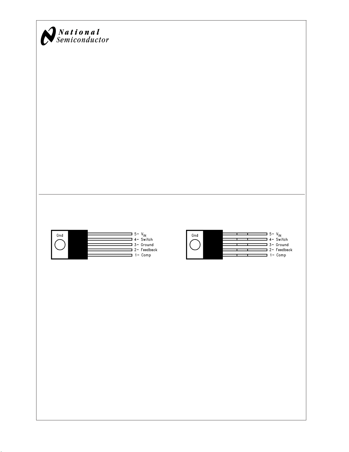
5-Lead Surface-Mount Package
Top View
or LM2577N-ADJ
TO-263 (S)
Top View
01146806
01146832
*No internal Connection
01146807
Top View
Order Number LM2577M-12, LM2577M-15,
or LM2577M-ADJ
See NS Package Number M24B
01146833
Side View
Order Number LM2577S-12, LM2577S-15,
or LM2577S-ADJ
See NS Package Number TS5B
4-Lead TO-3 (K)
Bottom View
Order Number LM1577K-12/883, LM1577K-15/883,
or LM1577K-ADJ/883
See NS Package Number K04A
www.national.com 2
01146808
Ordering Information
LM1577/LM2577
Temperature
Range
−40˚C ≤ T
≤ +125˚C 24-Pin Surface
A
Mount
16-Pin Molded DIP LM2577N-12 LM2577N-15 LM2577N-ADJ N16A N
5-Lead Surface
Mount
5-Straight Leads LM2577T-12 LM2577T-15 LM2577T-ADJ T05A TO-220
5-Bent Staggered LM2577T-12 LM2577T-15 LM2577T-ADJ T05D TO-220
Leads Flow LB03 Flow LB03 Flow LB03
−55˚C ≤ T
≤ +150˚C 4-Pin TO-3 LM1577K-12/883LM1577K-15/883 LM1577K-
A
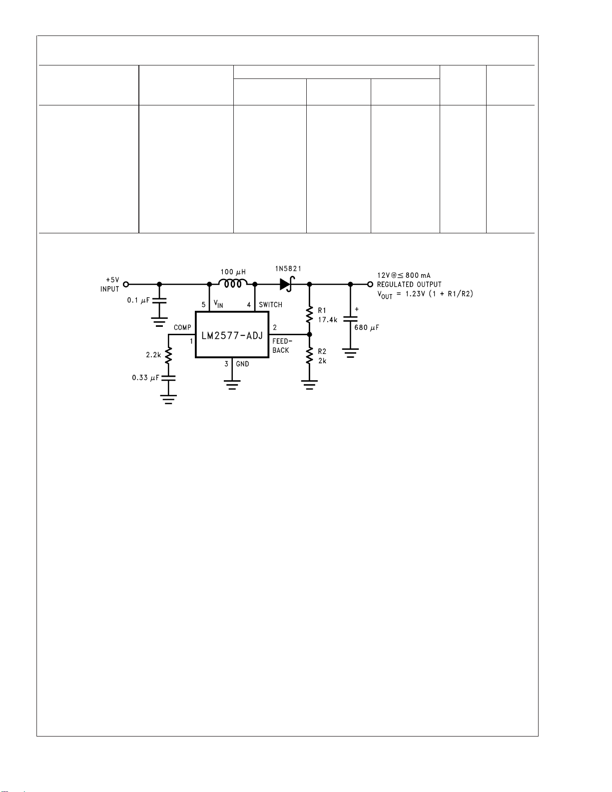
Typical Application
Package
Type
Output Voltage NSC
12V 15V ADJ Package Package
Drawing
LM2577M-12 LM2577M-15 LM2577M-ADJ M24B SO
LM2577S-12 LM2577S-15 LM2577S-ADJ TS5B TO-263
K04A TO-3
ADJ/883
Note: Pin numbers shown are for TO-220 (T) package.
01146801
www.national.com3
Absolute Maximum Ratings (Note 1)
If Military/Aerospace specified devices are required,
Minimum ESD Rating
(C = 100 pF, R = 1.5 kΩ)2kV
please contact the National Semiconductor Sales Office/
Distributors for availability and specifications.
Operating Ratings
Supply Voltage 45V
LM1577/LM2577
Output Switch Voltage 65V
Output Switch Current (Note 2) 6.0A
Power Dissipation Internally Limited
Storage Temperature Range −65˚C to +150˚C
Lead Temperature
(Soldering, 10 sec.) 260˚C
Supply Voltage 3.5V ≤ VIN≤ 40V
Output Switch Voltage 0V ≤ V
Output Switch Current I
SWITCH
Junction Temperature Range
LM1577 −55˚C ≤ T
LM2577 −40˚C ≤ T
Maximum Junction Temperature 150˚C
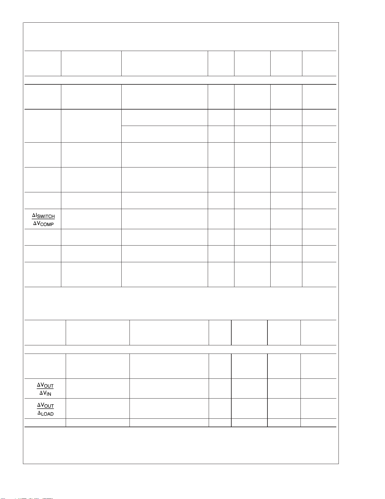
Electrical Characteristics—LM1577-12, LM2577-12
Specifications with standard type face are for TJ= 25˚C, and those in bold type face apply over full Operating Temperature
Range. Unless otherwise specified, V
= 5V, and I
IN
Symbol Parameter Conditions Typical Limit Limit (Limits)
SYSTEM PARAMETERS Circuit of Figure 1 (Note 6)
V
OUT
Output Voltage VIN= 5V to 10V 12.0 V
I
= 100 mA to 800 mA 11.60/11.40 11.60/11.40 V(min)
LOAD
(Note 3) 12.40/12.60 12.40/12.60 V(max)
Line Regulation VIN= 3.5V to 10V 20 mV
I
= 300 mA 50/100 50/100 mV(max)
LOAD
Load Regulation VIN=5V 20 mV
I
= 100 mA to 800 mA 50/100 50/100 mV(max)
LOAD
η Efficiency V
= 5V, I
IN
LOAD
DEVICE PARAMETERS
I
S
V
UV
Input Supply Current V
Input Supply I
FEEDBACK
I
SWITCH
V
COMP
SWITCH
= 14V (Switch Off) 7.5 mA
= 2.0A 25 mA
= 2.0V (Max Duty Cycle) 50/85 50/85 mA(max)
= 100 mA 2.90 V
Undervoltage Lockout 2.70/2.65 2.70/2.65 V(min)
f
O
V
REF
Oscillator Frequency Measured at Switch Pin 52 kHz
I
= 100 mA 48/42 48/42 kHz(min)
SWITCH
Output Reference Measured at Feedback Pin V
Voltage V
= 3.5V to 40V 12 11.76/11.64 11.76/11.64 V(min)
IN
V
= 1.0V 12.24/12.36 12.24/12.36 V(max)
COMP
Output Reference VIN= 3.5V to 40V
Voltage Line Regulator
R
FB
Feedback Pin Input 9.7 kΩ
Resistance
G
M
Error Amp I
Transconductance V
= −30 µA to +30 µA 370 µmho
COMP
= 1.0V 225/145 225/145 µmho(min)
COMP
=0.
SWITCH
LM1577-12 LM2577-12 Units
(Notes 3, 4) (Note 5)
= 800 mA 80 %
10.0/14.0 10.0/14.0 mA(max)
3.10/3.15 3.10/3.15 V(max)
56/62 56/62 kHz(max)
7mV
515/615 515/615 µmho(max)
SWITCH
J
J
≤ 60V
≤ 3.0A
≤ +150˚C
≤ +125˚C
www.national.com 4
Electrical Characteristics— LM1577-12, LM2577-12 (Continued)
Specifications with standard type face are for TJ= 25˚C, and those in bold type face apply over full Operating Temperature
Range. Unless otherwise specified, V
= 5V, and I
IN
Symbol Parameter Conditions Typical Limit Limit (Limits)
DEVICE PARAMETERS
A
VOL
Error Amp V
Voltage Gain R
= 1.1V to 1.9V 80 V/V
COMP
= 1.0 MΩ 50/25 50/25 V/V(min)
COMP
(Note 7)
Error Amplifier Upper Limit 2.4 V
Output Swing V
FEEDBACK
= 10.0V 2.2/2.0 2.2/2.0 V(min)
Lower Limit 0.3 V
Error Amplifier V
Output Current V
I
SS
Soft Start Current V
D Maximum Duty Cycle V
V
FEEDBACK
FEEDBACK
COMP
FEEDBACK
V
COMP
COMP
I
SWITCH
= 15.0V 0.40/0.55 0.40/0.55 V(max)
= 10.0V to 15.0V
= 1.0V
= 10.0V 5.0 µA
= 0V 2.5/1.5 2.5/1.5 µA(min)
= 1.5V 95 %
= 100 mA 93/90 93/90 %(min)
Switch
Transconductance
SWITCH
=0.
LM1577-12 LM2577-12 Units
(Notes 3, 4) (Note 5)
±
200 µA
±
130/±90
±
300/±400±300/±400 µA(max)
±
130/±90 µA(min)
7.5/9.5 7.5/9.5 µA(max)
12.5 A/V
LM1577/LM2577
I
L
Switch Leakage V
Current V
V
SAT
Switch Saturation I
SWITCH
Voltage V
= 65V 10 µA
SWITCH
FEEDBACK
= 15V (Switch Off) 300/600 300/600 µA(max)
= 2.0A 0.5 V
= 2.0V (Max Duty Cycle) 0.7/0.9 0.7/0.9 V(max)
COMP
NPN Switch 4.5 A
Current Limit 3.7/3.0 3.7/3.0 A(min)
5.3/6.0 5.3/6.0 A(max)
Electrical Characteristics— LM1577-15, LM2577-15
Specifications with standard type face are for TJ= 25˚C, and those in bold type face apply over full Operating Temperature
Range. Unless otherwise specified, V
= 5V, and I
IN
Symbol Parameter Conditions Typical Limit Limit (Limits)
SYSTEM PARAMETERS Circuit of Figure 2 (Note 6)
V
OUT
Output Voltage VIN= 5V to 12V 15.0 V
I
= 100 mA to 600 mA 14.50/14.25 14.50/14.25 V(min)
LOAD
(Note 3) 15.50/15.75 15.50/15.75 V(max)
Line Regulation VIN= 3.5V to 12V 20
= 300 mA mV(max)
I
LOAD
Load Regulation VIN=5V 20
I
= 100 mA to 600 mA mV(max)
LOAD
η Efficiency V
IN
= 5V, I
=0.
SWITCH
LM1577-15 LM2577-15 Units
(Notes 3, 4) (Note 5)
50/100 50/100
50/100 50/100
= 600 mA 80 %
LOAD
mV
mV
www.national.com5
Electrical Characteristics— LM1577-15, LM2577-15 (Continued)
Specifications with standard type face are for TJ= 25˚C, and those in bold type face apply over full Operating Temperature
Range. Unless otherwise specified, V
= 5V, and I
IN
Symbol Parameter Conditions Typical Limit Limit (Limits)
LM1577/LM2577
DEVICE PARAMETERS
I
S
V
UV
f
O
V
REF
R
FB
G
M
A
VOL
I
SS
D Maximum Duty V
Input Supply Current V
FEEDBACK
(Switch Off) 10.0/14.0 10.0/14.0 mA(max)
I
V
= 2.0A 25 mA
SWITCH
= 2.0V 50/85 50/85 mA(max)
COMP
(Max Duty Cycle)
Input Supply I
= 100 mA 2.90 V
SWITCH
Undervoltage 2.70/2.65 2.70/2.65 V(min)
Lockout 3.10/3.15 3.10/3.15 V(max)
Oscillator Frequency Measured at Switch Pin 52 kHz
I
= 100 mA 48/42 48/42 kHz(min)
SWITCH
Output Reference Measured at Feedback Pin V
Voltage V
= 3.5V to 40V 15 14.70/14.55 14.70/14.55 V(min)
IN
V
= 1.0V 15.30/15.45 15.30/15.45 V(max)
COMP
Output Reference VIN= 3.5V to 40V 10 mV
Voltage Line Regulation
Feedback Pin Input 12.2 kΩ
Voltage Line Regulator
Error Amp I
Transconductance V
Error Amp V
Voltage Gain R
= −30 µA to +30 µA 300 µmho
COMP
= 1.0V 170/110 170/110 µmho(min)
COMP
= 1.1V to 1.9V 65 V/V
COMP
= 1.0 MΩ 40/20 40/20 V/V(min)
COMP
(Note 7)
Error Amplifier Upper Limit 2.4 V
Output Swing V
FEEDBACK
Lower Limit 0.3 V
V
FEEDBACK
Error Amp V
Output Current V
Soft Start Current V
Cycle I
FEEDBACK
= 1.0V
COMP
FEEDBACK
V
= 0V 2.5/1.5 2.5/1.5 µA(min)
COMP
= 1.5V 95 %
COMP
= 100 mA 93/90 93/90 %(min)
SWITCH
Switch
Transconductance
=0.
SWITCH
LM1577-15 LM2577-15 Units
(Notes 3, 4) (Note 5)
= 18.0V 7.5 mA
56/62 56/62 kHz(max)
420/500 420/500 µmho(max)
= 12.0V 2.2/2.0 2.2/2.0 V(min)
= 18.0V 0.4/0.55 0.40/0.55 V(max)
= 12.0V to 18.0V
±
200 µA
±
130/±90
±
300/±400±300/±400 µA(max)
±
130/±90 µA(min)
= 12.0V 5.0 µA
7.5/9.5 7.5/9.5 µA(max)
12.5 A/V
I
L
Switch Leakage V
Current V
= 65V 10 µA
SWITCH
FEEDBACK
= 18.0V 300/600 300/600 µA(max)
(Switch Off)
V
SAT
Switch Saturation I
Voltage V
= 2.0A 0.5 V
SWITCH
= 2.0V 0.7/0.9 0.7/0.9 V(max)
COMP
(Max Duty Cycle)
www.national.com 6
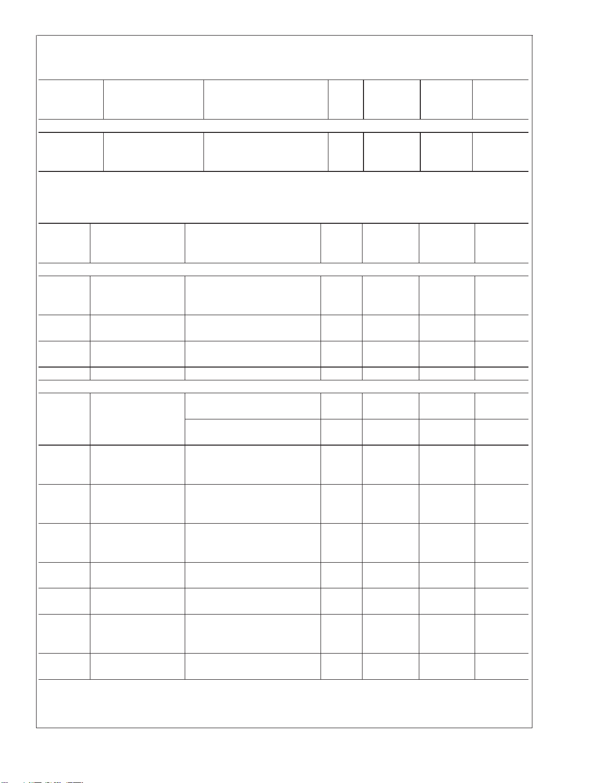
Electrical Characteristics— LM1577-15, LM2577-15 (Continued)
Specifications with standard type face are for TJ= 25˚C, and those in bold type face apply over full Operating Temperature
Range. Unless otherwise specified, V
= 5V, and I
IN
SWITCH
=0.
LM1577-15 LM2577-15 Units
Symbol Parameter Conditions Typical Limit Limit (Limits)
(Notes 3, 4) (Note 5)
DEVICE PARAMETERS
NPN Switch V
= 2.0V 4.3 A
COMP
Current Limit 3.7/3.0 3.7/3.0 A(min)
5.3/6.0 5.3/6.0 A(max)
Electrical Characteristics— LM1577-ADJ, LM2577-ADJ
Specifications with standard type face are for TJ= 25˚C, and those in bold type face apply over full Operating Temperature
Range. Unless otherwise specified, V
= 5V, V
IN
FEEDBACK
Symbol Parameter Conditions Typical Limit Limit (Limits)
SYSTEM PARAMETERS Circuit of Figure 3 (Note 6)
V
OUT
Output Voltage VIN= 5V to 10V 12.0 V
I
= 100 mA to 800 mA 11.60/11.40 11.60/11.40 V(min)
LOAD
(Note 3) 12.40/12.60 12.40/12.60 V(max)
∆V
/ Line Regulation VIN= 3.5V to 10V 20 mV
OUT
∆V
IN
∆V
/ Load Regulation VIN=5V 20 mV
OUT
∆I
LOAD
η Efficiency V
I
= 300 mA 50/100 50/100 mV(max)
LOAD
I
= 100 mA to 800 mA 50/100 50/100 mV(max)
LOAD
= 5V, I
IN
LOAD
DEVICE PARAMETERS
I
S
V
UV
Input Supply Current V
Input Supply I
FEEDBACK
I
SWITCH
V
COMP
SWITCH
= 1.5V (Switch Off) 7.5 mA
= 2.0A 25 mA
= 2.0V (Max Duty Cycle) 50/85 50/85 mA(max)
= 100 mA 2.90 V
Undervoltage Lockout 2.70/2.65 2.70/2.65 V(min)
f
O
V
∆V
∆V
I
B
REF
REF
IN
Oscillator Frequency Measured at Switch Pin 52 kHz
I
= 100 mA 48/42 48/42 kHz(min)
SWITCH
Reference Measured at Feedback Pin V
Voltage V
= 3.5V to 40V 1.230 1.214/1.206 1.214/1.206 V(min)
IN
V
= 1.0V 1.246/1.254 1.246/1.254 V(max)
COMP
/ Reference Voltage VIN= 3.5V to 40V 0.5 mV
Line Regulation
Error Amp V
= 1.0V 100 nA
COMP
Input Bias Current 300/800 300/800 nA(max)
G
M
A
VOL
Error Amp I
Transconductance V
Error Amp V
Voltage Gain R
= −30 µA to +30 µA 3700 µmho
COMP
= 1.0V 2400/1600 2400/1600 µmho(min)
COMP
= 1.1V to 1.9V 800 V/V
COMP
= 1.0 MΩ (Note 7) 500/250 500/250 V/V(min)
COMP
=V
REF
, and I
SWITCH
=0.
LM1577-ADJ LM2577-ADJ Units
(Notes 3, 4) (Note 5)
= 800 mA 80 %
10.0/14.0 10.0/14.0 mA(max)
3.10/3.15 3.10/3.15 V(max)
56/62 56/62 kHz(max)
4800/5800 4800/5800 µmho(max)
LM1577/LM2577
www.national.com7
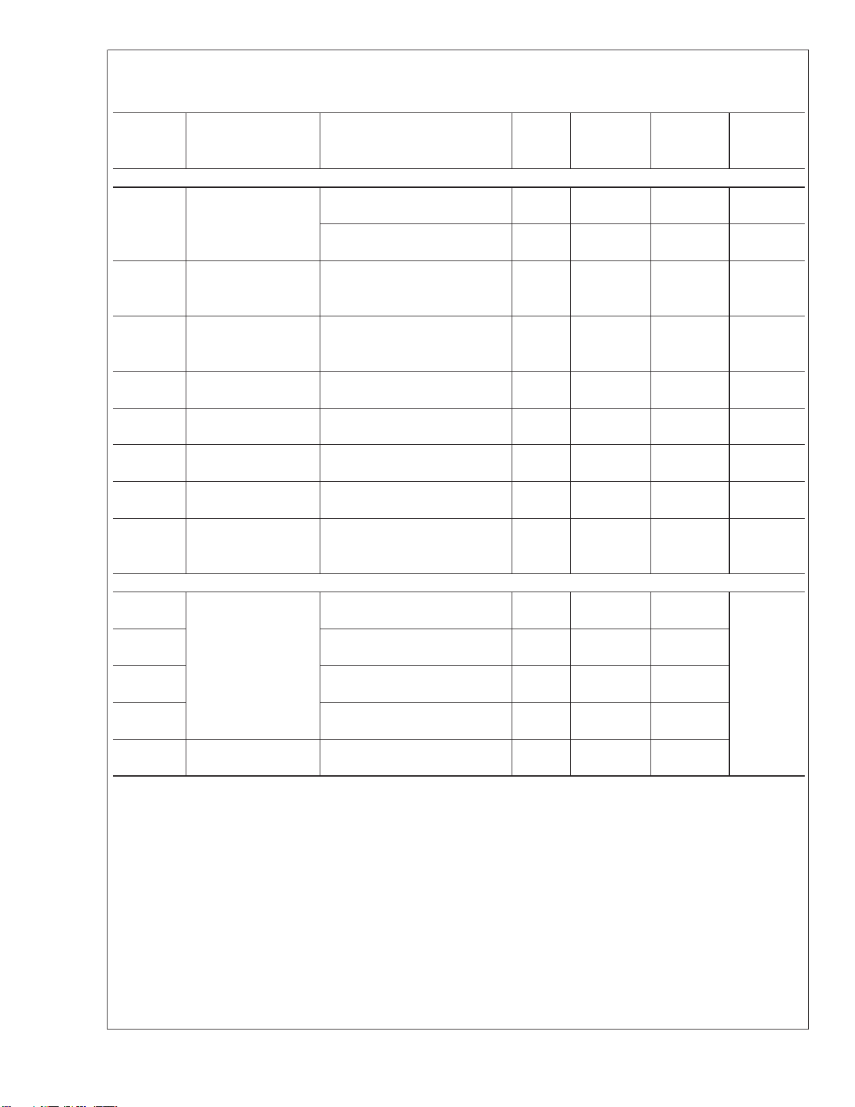
Electrical Characteristics— LM1577-ADJ, LM2577-ADJ (Continued)
Specifications with standard type face are for TJ= 25˚C, and those in bold type face apply over full Operating Temperature
Range. Unless otherwise specified, V
= 5V, V
IN
FEEDBACK
Symbol Parameter Conditions Typical Limit Limit (Limits)
LM1577/LM2577
DEVICE PARAMETERS
Error Amplifier Upper Limit 2.4 V
Output Swing V
FEEDBACK
Lower Limit 0.3 V
V
FEEDBACK
Error Amp V
Output Current V
I
SS
Soft Start Current V
D Maximum Duty Cycle V
∆I
∆V
I
L
/ Switch 12.5 A/V
SWITCH
COMP
Transconductance
Switch Leakage V
Current V
V
SAT
Switch Saturation I
Voltage V
NPN Switch V
FEEDBACK
COMP
FEEDBACK
V
COMP
COMP
I
SWITCH
SWITCH
FEEDBACK
SWITCH
COMP
COMP
Current Limit 3.7/3.0 3.7/3.0 A(min)
THERMAL PARAMETERS (All Versions)
θ
JA
θ
JC
θ
JA
θ
JC
θ
JA
Thermal Resistance K Package, Junction to Ambient 35
K Package, Junction to Case 1.5
T Package, Junction to Ambient 65
T Package, Junction to Case 2
N Package, Junction to 85
Ambient (Note 8)
θ
JA
M Package, Junction 100
to Ambient (Note 8)
θ
JA
S Package, Junction to 37
Ambient (Note 9)
Note 1: Absolute Maximum Ratings indicate limits beyond which damage to the device may occur. Operating ratings indicate conditions the device is intended to
be functional, but device parameter specifications may not be guaranteed under these conditions. For guaranteed specifications and test conditions, see the
Electrical Characteristics.
Note 2: Due to timing considerations of the LM1577/LM2577 current limit circuit, output current cannot be internally limited when the LM1577/LM2577 is used as
a step-up regulator. To prevent damage to the switch, its current must be externally limited to 6.0A. However, output current is internally limited when the
LM1577/LM2577 is used as a flyback or forward converter regulator in accordance to the Application Hints.
Note 3: All limits guaranteed at room temperature (standard type face) and at temperature extremes (boldface type). All limits are used to calculate Outgoing Quality
Level, and are 100% production tested.
Note 4: A military RETS electrical test specification is available on request. At the time of printing, the LM1577K-12/883, LM1577K-15/883, and LM1577K-ADJ/883
RETS specifications complied fully with the boldface limits in these columns. The LM1577K-12/883, LM1577K-15/883, and LM1577K-ADJ/883 may also be procured
to Standard Military Drawing specifications.
Note 5: All limits guaranteed at room temperature (standard type face) and at temperature extremes (boldface type). All room temperature limits are 100%
production tested. All limits at temperature extremes are guaranteed via correlation using standard Statistical Quality Control (SQC) methods.
Note 6: External components such as the diode, inductor, input and output capacitors can affect switching regulator performance. When the LM1577/LM2577 is
used as shown in the Test Circuit, system performance will be as specified by the system parameters.
Note 7: A 1.0 MΩ resistor is connected to the compensation pin (which is the error amplifier’s output) to ensure accuracy in measuring A
this pin’s load resistance should be ≥10 MΩ, resulting in A
= 1.0V 2.2/2.0 2.2/2.0 V(min)
= 1.5V 0.40/0.55 0.40/0.55 V(max)
= 1.0V to 1.5V
= 1.0V
= 1.0V 5.0 µA
= 0V 2.5/1.5 2.5/1.5 µA(min)
= 1.5V 95 %
= 100 mA 93/90 93/90 %(min)
= 65V 10 µA
= 1.5V (Switch Off) 300/600 300/600 µA(max)
= 2.0A 0.5 V
= 2.0V (Max Duty Cycle) 0.7/0.9 0.7/0.9 V(max)
= 2.0V 4.3 A
that is typically twice the guaranteed minimum limit.
VOL
=V
REF
, and I
=0.
SWITCH
LM1577-ADJ LM2577-ADJ Units
(Notes 3, 4) (Note 5)
±
200 µA
±
130/±90
±
300/±400±300/±400 µA(max)
±
130/±90 µA(min)
7.5/9.5 7.5/9.5 µA(max)
5.3/6.0 5.3/6.0 A(max)
. In actual applications,
VOL
˚C/W
www.national.com 8
Electrical Characteristics— LM1577-ADJ, LM2577-ADJ (Continued)
Note 8: Junction to ambient thermal resistance with approximately 1 square inch of pc board copper surrounding the leads. Additional copper area will lower thermal
resistance further. See thermal model in “Switchers Made Simple” software.
Note 9: If the TO-263 package is used, the thermal resistance can be reduced by increasing the PC board copper area thermally connected to the package. Using
0.5 square inches of copper area, θ
is 50˚C/W; with 1 square inch of copper area, θJAis 37˚C/W; and with 1.6 or more square inches of copper area, θJAis 32˚C/W.
JA
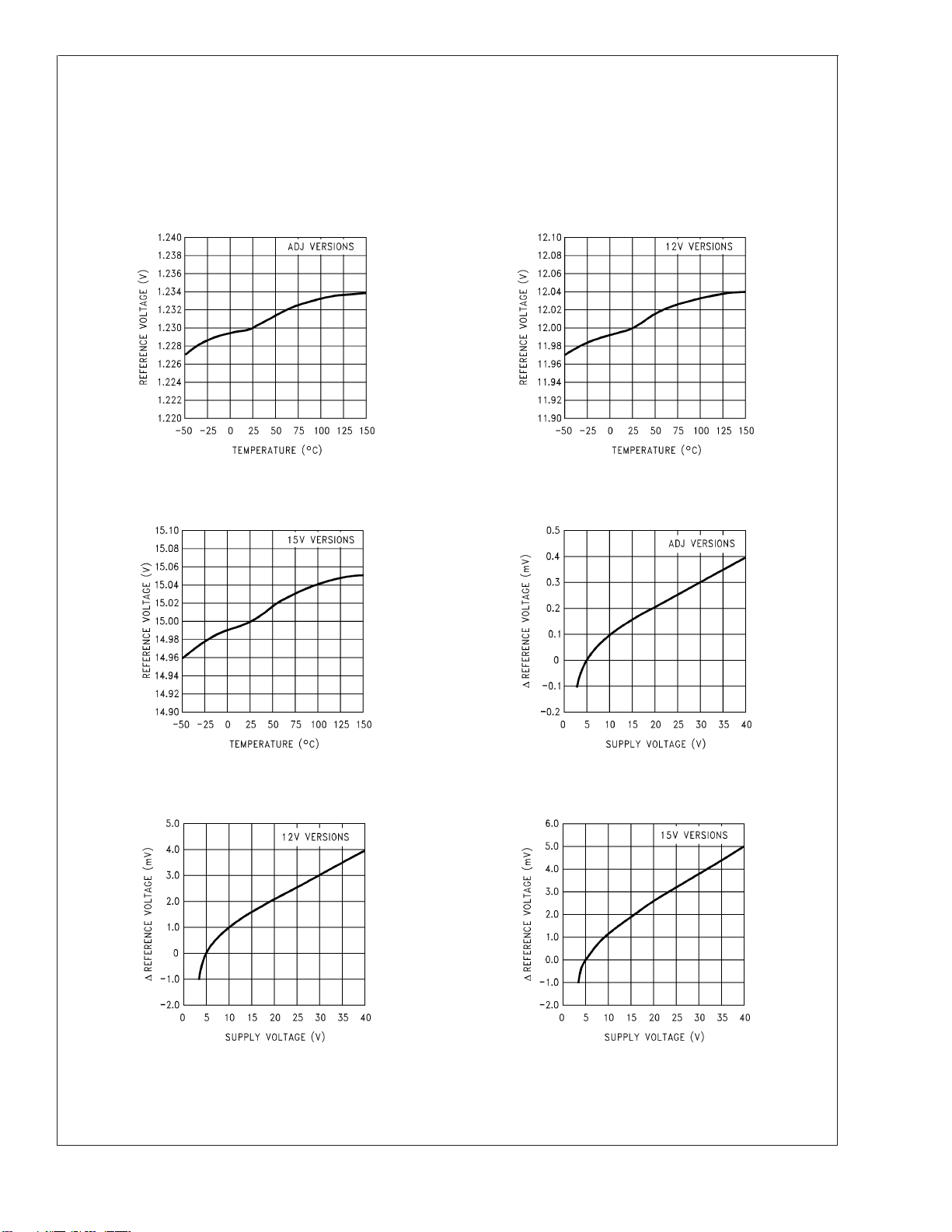
Typical Performance Characteristics
LM1577/LM2577
Reference Voltage
vs Temperature
Reference Voltage
vs Temperature
Reference Voltage
vs Temperature
01146834 01146835
∆ Reference Voltage
vs Supply Voltage
∆ Reference Voltage
vs Supply Voltage
01146836 01146837
∆ Reference Voltage
vs Supply Voltage
01146838
01146839
www.national.com9
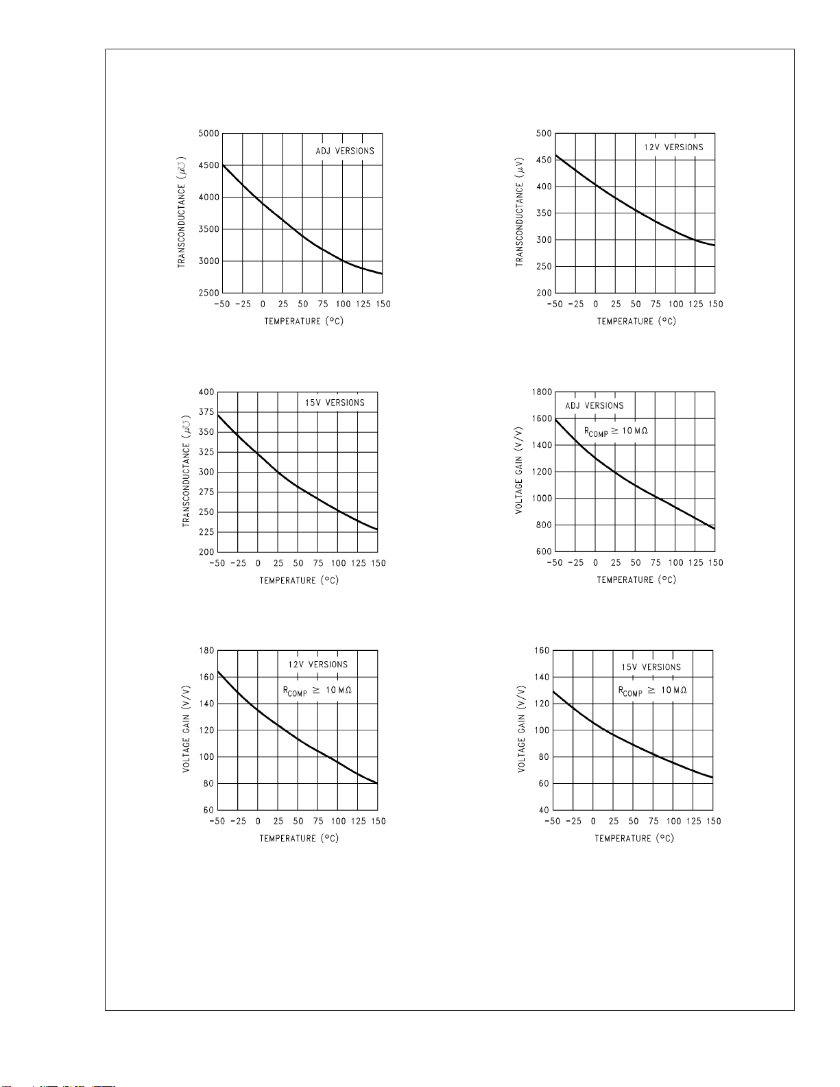
Typical Performance Characteristics (Continued)
LM1577/LM2577
Error Amp Transconductance
vs Temperature
Error Amp Transconductance
vs Temperature
01146840
Error Amp Transconductance
vs Temperature
01146841
Error Amp Voltage
Gain vs Temperature
Error Amp Voltage
Gain vs Temperature
01146842
01146843
Error Amp Voltage
Gain vs Temperature
01146844 01146845
www.national.com 10
 Loading...