


LM2524D/LM3524D
Regulating Pulse Width Modulator
General Description
The LM3524D family is an improved version of the industry
standard LM3524. It has improved specifications and additional features yet is pin for pin compatible with existing 3524
families. New features reduce the need for additional external
circuitry often required in the original version.
The LM3524D has a ±1% precision 5V reference. The current
carrying capability of the output drive transistors has been
raised to 200 mA while reducing V
breakdown to 60V. The common mode voltage range of the
error-amp has been raised to 5.5V to eliminate the need for
a resistive divider from the 5V reference.
In the LM3524D the circuit bias line has been isolated from
the shut-down pin. This prevents the oscillator pulse amplitude and frequency from being disturbed by shut-down. Also
at high frequencies (≃300 kHz) the max. duty cycle per output
has been improved to 44% compared to 35% max. duty cycle
in other 3524s.
In addition, the LM3524D can now be synchronized externally, through pin 3. Also a latch has been added to insure one
and increasing V
CEsat
pulse per period even in noisy environments. The LM3524D
includes double pulse suppression logic that insures when a
shut-down condition is removed the state of the T-flip-flop will
change only after the first clock pulse has arrived. This feature
prevents the same output from being pulsed twice in a row,
thus reducing the possibility of core saturation in push-pull
designs.
Features
CE
Fully interchangeable with standard LM3524 family
■
±1% precision 5V reference with thermal shut-down
■
Output current to 200 mA DC
■
60V output capability
■
Wide common mode input range for error-amp
■
One pulse per period (noise suppression)
■
Improved max. duty cycle at high frequencies
■
Double pulse suppression
■
Synchronize through pin 3
■
LM2524D/LM3524D Regulating Pulse Width Modulator
May 2, 2008
Connection Diagram
Order Number LM2524DN or LM3524DN
Top View
See NS Package Number N16E
Order Number LM3524DM
See NS Package Number M16A
865002
© 2008 National Semiconductor Corporation 8650 www.national.com
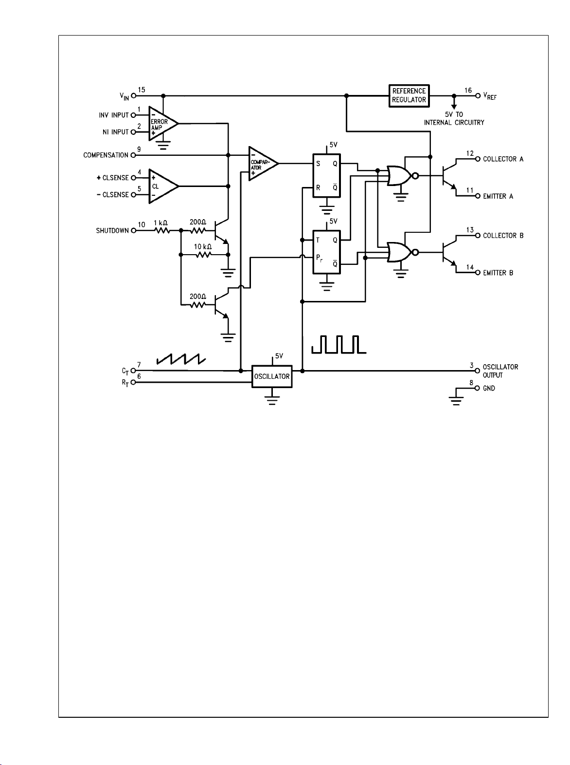
Block Diagram
LM2524D/LM3524D
865001
www.national.com 2

LM2524D/LM3524D
Absolute Maximum Ratings (Note 5)
If Military/Aerospace specified devices are required,
please contact the National Semiconductor Sales Office/
Distributors for availability and specifications.
Supply Voltage 40V
Collector Supply Voltage
(LM2524D) 55V
(LM3524D) 40V
Output Current DC (each) 200 mA
Internal Power Dissipation 1W
Operating Junction Temperature
Range (Note 2)
LM2524D −40°C to +125°C
LM3524D 0°C to +125°C
Maximum Junction Temperature 150°
Storage Temperature Range −65°C to +150°C
Lead Temperature (Soldering 4 sec.)
M, N Pkg. 260°C
Oscillator Charging Current (Pin 7) 5 mA
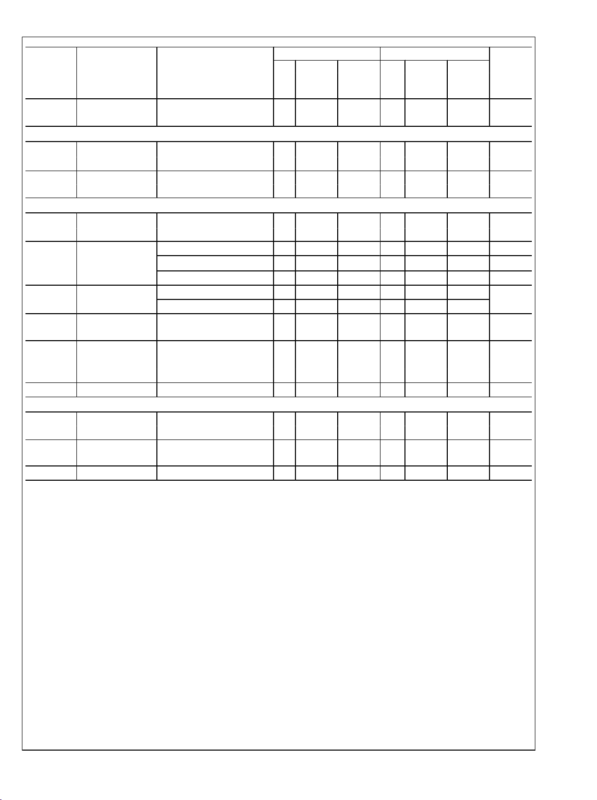
Electrical Characteristics
(Note 1)
LM2524D LM3524D
Symbol Parameter Conditions
Typ Limit Limit Typ Limit Limit
REFERENCE SECTION
V
REF
Output Voltage
V
V
RLine
RLoad
Line Regulation VIN = 8V to 40V 10 15 30 10 25 50 mV
Load Regulation IL = 0 mA to 20 mA 10 15 25 10 25 50 mV
Ripple Rejection f = 120 Hz 66 66 dB
Tested Design Tested Design
(Note 3) (Note 4)
4.85 4.80
5
5.15 5.20
(Note 3) (Note 4)
4.75 V
5
5.25 V
Units
Min
Max
Max
Max
I
OS
Short Circuit V
= 0 25 25 mA Min
REF
Current 50 50
180 200 mA Max
N
O
Output Noise
10 Hz ≤ f ≤ 10 kHz
Long Term TA = 125°C
40 100 40 100
20
20
Stability
OSCILLATOR SECTION
f
OSC
Max. Freq.
RT = 1k, CT = 0.001 μF
550
500 350
(Note 7)
f
OSC
Initial
RT = 5.6k, CT = 0.01 μF
17.5 17.5 kHz
Accuracy (Note 7) 20 20
22.5 22.5 kHz
RT = 2.7k, CT = 0.01 μF
34 30 kHz
(Note 7) 38 38
42 46 kHz
Δf
OSC
with V
Δf
OSC
Freq. Change VIN = 8 to 40V
IN
0.5 1
Freq. Change TA = −55°C to +125°C
0.5 1.0
with Temp. at 20 kHz RT = 5.6k, 5 5 %
V
OSC
Output Amplitude
CT = 0.01 μF
RT = 5.6k, CT = 0.01 μF
3 2.4
3 2.4
(Pin 3) (Note 8)
t
PW
Output Pulse
RT = 5.6k, CT = 0.01 μF
0.5 1.5
0.5 1.5
Width (Pin 3)
Sawtooth Peak
RT = 5.6k, CT = 0.01 μF
3.4 3.6 3.8
3.8
Voltage
μV
rms Max
mV/kHr
kHz
%
Max
V
Min
μs
Max
V
Max
Min
Min
Max
Min
Max
3 www.national.com

LM2524D LM3524D
Symbol Parameter Conditions
Tested Design Tested Design
Typ Limit Limit Typ Limit Limit
Sawtooth Valley
RT = 5.6k, CT = 0.01 μF
(Note 3) (Note 4)
1.1 0.8 0.6
(Note 3) (Note 4)
0.6
Voltage
LM2524D/LM3524D
ERROR-AMP SECTION
V
IO
Input Offset VCM = 2.5V
2 8 10 2 10
mV
Voltage
I
IB
Input Bias VCM = 2.5V
1 8 10 1 10
Current
I
IO
Input Offset VCM = 2.5V
0.5 1.0 1 0.5 1
Current
I
COSI
Compensation V
IN(I)
− V
= 150 mV 65 65
IN(NI)
Current (Sink) 95 95
125 125
I
COSO
Compensation V
IN(NI)
− V
= 150 mV −125 −125
IN(I)
Current (Source) −95 −95
−65 −65
A
VOL
Open Loop Gain
RL = ∞, VCM = 2.5 V
80 74 60 80 70 60 dB
VCMR Common Mode 1.5 1.4 1.5 V
Input Voltage
5.5 5.4 5.5 V
Range
CMRR Common Mode
90 80
90 80
dB
Rejection Ratio
G
BW
Unity Gain A
= 0 dB, VCM = 2.5V
VOL
3
2
Bandwidth
V
O
Output Voltage
RL = ∞
0.5 0.5 V
Swing 5.5 5.5 V
PSRR Power Supply VIN = 8 to 40V
80
70 80 65
db
Rejection Ratio
COMPARATOR SECTION
V
COMPZ
Minimum Duty Pin 9 = 0.8V,
Cycle
[RT = 5.6k, CT = 0.01 μF]
Maximum Duty Pin 9 = 3.9V,
Cycle
[RT = 5.6k, CT = 0.01 μF]
Maximum Duty Pin 9 = 3.9V,
Cycle
[RT = 1k, CT = 0.001 μF]
Input Threshold Zero Duty Cycle
0 0
49 45
44 35
1
0 0
49 45
44 35
1
%
%
%
(Pin 9)
V
COMPM
Input Threshold Maximum Duty Cycle
3.5
3.5
(Pin 9)
I
IB
Input Bias
−1
−1
Current
CURRENT LIMIT SECTION
V
SEN
Sense Voltage
V
(Pin 2)
− V
(Pin 1)
≥
180 180 mV
150 mV 200 200
220 220 mV
TC-V
sense
Sense Voltage T.C. 0.2 0.2 mV/°C
Units
V
Min
Max
μA
Max
μA
Max
μA
Min
μA
Max
μA
Min
μA
Max
Min
Min
Max
Min
MHz
Min
Max
Min
Max
Min
Min
V
V
μA
Min
Max
www.national.com 4
LM2524D LM3524D
Symbol Parameter Conditions
Tested Design Tested Design
Units
Typ Limit Limit Typ Limit Limit
(Note 3) (Note 4)
(Note 3) (Note 4)
Common Mode −0.7 −0.7 V
Voltage Range V5 − V4 = 300 mV 1 1 V
SHUT DOWN SECTION
V
SD
High Input
V
(Pin 2)
− V
(Pin 1)
≥
1
0.5
0.5 V
1
Voltage 150 mV 1.5 1.5 V
I
SD
High Input I
(pin 10)
1
1
mA
Current
OUTPUT SECTION (EACH OUTPUT)
V
CES
Collector Emitter
IC ≤ 100 μA
55
40
V
Voltage Breakdown
I
CES
V
CESAT
V
EO
Collector Leakage VCE = 60V
Current
VCE = 55V 0.1 50
VCE = 40V 0.1 50
Saturation IE = 20 mA 0.2 0.5 0.2 0.7
Voltage
Emitter Output IE = 50 mA
IE = 200 mA 1.5 2.2 1.5 2.5
18 17
18 17
μA
V
V
Voltage
t
R
Rise Time VIN = 20V,
IE = −250 μA
200 200 ns
RC = 2k
t
F
Fall Time RC = 2k 100 100 ns
SUPPLY CHARACTERISTICS SECTION
V
IN
Input Voltage After Turn-on 8 8 V
Range 40 40 V
T Thermal Shutdown (Note 2) 160 160 °C
Temp.
I
IN
Note 1: Unless otherwise stated, these specifications apply for TA = TJ = 25°C. Boldface numbers apply over the rated temperature range: LM2524D is −40° to
85°C and LM3524D is 0°C to 70°C. VIN = 20V and f
Note 2: For operation at elevated temperatures, devices in the N package must be derated based on a thermal resistance of 86°C/W, junction to ambient. Devices
in the M package must be derated at 125°C/W, junction to ambient.
Note 3: Tested limits are guaranteed and 100% tested in production.
Note 4: Design limits are guaranteed (but not 100% production tested) over the indicated temperature and supply voltage range. These limits are not used to
calculate outgoing quality level.
Note 5: Absolute maximum ratings indicate limits beyond which damage to the device may occur. DC and AC electrical specifications do not apply when operating
the device beyond its rated operating conditions.
Note 6: Pins 1, 4, 7, 8, 11, and 14 are grounded; Pin 2 = 2V. All other inputs and outputs open.
Note 7: The value of a Ct capacitor can vary with frequency. Careful selection of this capacitor must be made for high frequency operation. Polystyrene was used
in this test. NPO ceramic or polypropylene can also be used.
Note 8: OSC amplitude is measured open circuit. Available current is limited to 1 mA so care must be exercised to limit capacitive loading of fast pulses.
Stand By Current VIN = 40V (Note 6) 5 10 5 10 mA
= 20 kHz.
OSC
LM2524D/LM3524D
Min
Max
Min
Max
Min
Max
Max
Min
Min
Max
5 www.national.com
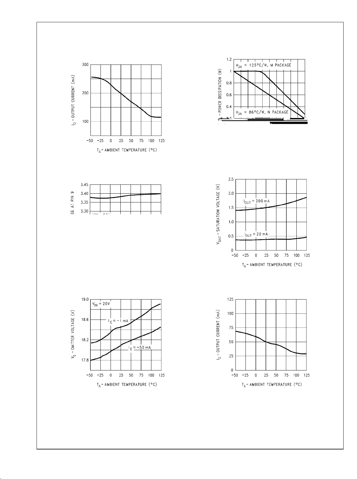
Typical Performance Characteristics
LM2524D/LM3524D
Switching Transistor
Peak Output Current
vs Temperature
Maximum & Minimum
Duty Cycle Threshold
Voltage
Maximum Average Power
Dissipation (N, M Packages)
865029
865028
Output Transistor
Saturation Voltage
Output Transistor Emitter
Voltage
865030
865032
865031
Reference Transistor
Peak Output Current
865033
www.national.com 6
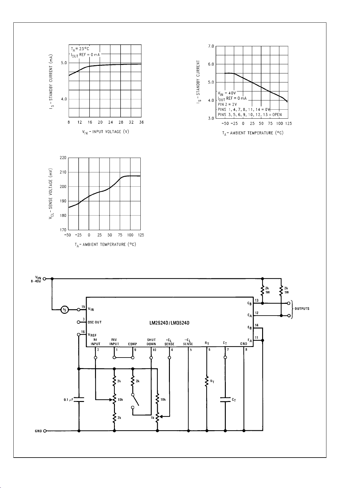
LM2524D/LM3524D
Standby Current
vs Voltage
Current Limit Sense Voltage
865034
Standby Current
vs Temperature
865035
Test Circuit
865036
865004
7 www.national.com

Functional Description
INTERNAL VOLTAGE REGULATOR
The LM3524D has an on-chip 5V, 50 mA, short circuit protected voltage regulator. This voltage regulator provides a
supply for all internal circuitry of the device and can be used
as an external reference.
For input voltages of less than 8V the 5V output should be
LM2524D/LM3524D
shorted to pin 15, VIN, which disables the 5V regulator. With
these pins shorted the input voltage must be limited to a maximum of 6V. If input voltages of 6V–8V are to be used, a preregulator, as shown in Figure 1, must be added.
865005
FIGURE 2.
*Minimum CO of 10 μF required for stability.
865010
FIGURE 1.
OSCILLATOR
The LM3524D provides a stable on-board oscillator. Its frequency is set by an external resistor, RT and capacitor, CT. A
graph of RT, CT vs oscillator frequency is shown is Figure 2.
The oscillator's output provides the signals for triggering an
internal flip-flop, which directs the PWM information to the
outputs, and a blanking pulse to turn off both outputs during
transitions to ensure that cross conduction does not occur.
The width of the blanking pulse, or dead time, is controlled by
the value of CT, as shown in Figure 3. The recommended
values of RT are 1.8 kΩ to 100 kΩ, and for CT, 0.001 μF to 0.1
μF.
If two or more LM3524D's must be synchronized together, the
easiest method is to interconnect all pin 3 terminals, tie all pin
7's (together) to a single CT, and leave all pin 6's open except
one which is connected to a single RT. This method works well
unless the LM3524D's are more than 6≃ apart.
A second synchronization method is appropriate for any circuit layout. One LM3524D, designated as master, must have
its RTCT set for the correct period. The other slave LM3524D
(s) should each have an RTCT set for a 10% longer period. All
pin 3's must then be interconnected to allow the master to
properly reset the slave units.
The oscillator may be synchronized to an external clock
source by setting the internal free-running oscillator frequency 10% slower than the external clock and driving pin 3 with
a pulse train (approx. 3V) from the clock. Pulse width should
be greater than 50 ns to insure full synchronization.
865006
FIGURE 3.
ERROR AMPLIFIER
The error amplifier is a differential input, transconductance
amplifier. Its gain, nominally 86 dB, is set by either feedback
or output loading. This output loading can be done with either
purely resistive or a combination of resistive and reactive
components. A graph of the amplifier's gain vs output load
resistance is shown in Figure 4.
www.national.com 8
865007
FIGURE 4.

LM2524D/LM3524D
The output of the amplifier, or input to the pulse width modulator, can be overridden easily as its output impedance is very
high (ZO ≃ 5 MΩ). For this reason a DC voltage can be applied
to pin 9 which will override the error amplifier and force a particular duty cycle to the outputs. An example of this could be
a non-regulating motor speed control where a variable voltage was applied to pin 9 to control motor speed. A graph of
the output duty cycle vs the voltage on pin 9 is shown in Figure
5.
The duty cycle is calculated as the percentage ratio of each
output's ON-time to the oscillator period. Paralleling the outputs doubles the observed duty cycle.
CURRENT LIMITING
The function of the current limit amplifier is to override the
error amplifier's output and take control of the pulse width.
The output duty cycle drops to about 25% when a current limit
sense voltage of 200 mV is applied between the +CL and
−CLsense terminals. Increasing the sense voltage approximately 5% results in a 0% output duty cycle. Care should be
taken to ensure the −0.7V to +1.0V input common-mode
range is not exceeded.
In most applications, the current limit sense voltage is produced by a current through a sense resistor. The accuracy of
this measurement is limited by the accuracy of the sense resistor, and by a small offset current, typically 100 μA, flowing
from +CL to −CL.
OUTPUT STAGES
The outputs of the LM3524D are NPN transistors, capable of
a maximum current of 200 mA. These transistors are driven
180° out of phase and have non-committed open collectors
and emitters as shown in Figure 6.
865008
FIGURE 5.
The amplifier's inputs have a common-mode input range of
1.5V–5.5V. The on board regulator is useful for biasing the
inputs to within this range.
865009
FIGURE 6.
9 www.national.com

Typical Applications
LM2524D/LM3524D
865011
FIGURE 7. Positive Regulator, Step-Up Basic Configuration (I
IN(MAX)
FIGURE 8. Positive Regulator, Step-Up Boosted Current Configuration
= 80 mA)
865012
www.national.com 10

865013
LM2524D/LM3524D
FIGURE 9. Positive Regulator, Step-Down Basic Configuration (I
11 www.national.com
IN(MAX)
= 80 mA)

LM2524D/LM3524D
865014
FIGURE 10. Positive Regulator, Step-Down Boosted Current Configuration
FIGURE 11. Boosted Current Polarity Inverter
www.national.com 12
865015

LM2524D/LM3524D
BASIC SWITCHING REGULATOR THEORY AND APPLICATIONS
The basic circuit of a step-down switching regulator circuit is
shown in Figure 12, along with a practical circuit design using
the LM3524D in Figure 15.
865016
FIGURE 12. Basic Step-Down Switching Regulator
The circuit works as follows: Q1 is used as a switch, which
has ON and OFF times controlled by the pulse width modulator. When Q1 is ON, power is drawn from VIN and supplied
to the load through L1; VA is at approximately VIN, D1 is reverse biased, and Co is charging. When Q1 turns OFF the
inductor L1 will force VA negative to keep the current flowing
in it, D1 will start conducting and the load current will flow
through D1 and L1. The voltage at VAis smoothed by the L1,
Co filter giving a clean DC output. The current flowing through
L1 is equal to the nominal DC load current plus some ΔI
which is due to the changing voltage across it. A good rule of
thumb is to set ΔI
≃ 40% × Io.
LP-P
865017
L
FIGURE 13. Relation of Switch Timing to Inductor Current in Step-Down Regulator
−
+
;
Neglecting V
, VD, and settling ΔI
SAT
L
= ΔI
L
where T = Total Period
The above shows the relation between VIN, Vo and duty cycle.
as Q1 only conducts during tON.
ηMAX will be further decreased due to switching losses in Q1.
For this reason Q1 should be selected to have the maximum
possible fT, which implies very fast rise and fall times.
CALCULATING INDUCTOR L1
−
Since ΔIL+ = ΔI
= 0.4I
L
o
Solving the above for L1
The efficiency, η, of the circuit is:
where: L1 is in Henrys
f is switching frequency in Hz
13 www.national.com

Also, see LM1578 data sheet for graphical methods of inductor selection.
CALCULATING OUTPUT FILTER CAPACITOR Co:
Figure 13 shows L1's current with respect to Q1's tON and
t
times (VA is at the collector of Q1). This curent must flow
OFF
to the load and Co. Co's current will then be the difference
between IL, and Io.
LM2524D/LM3524D
Ico = IL − I
o
From Figure 13 it can be seen that current will be flowing into
Co for the second half of tON through the first half of t
time, tON/2 + t
The resulting ΔVc or ΔVo is described by:
/2. The current flowing for this time is ΔIL/4.
OFF
OFF
, or a
865019
FIGURE 14. Inductor Current Slope in Step-Down
Regulator
A complete step-down switching regulator schematic, using
the LM3524D, is illustrated in Figure 15. Transistors Q1 and
Q2 have been added to boost the output to 1A. The 5V regulator of the LM3524D has been divided in half to bias the
error amplifier's non-inverting input to within its commonmode range. Since each output transistor is on for half the
period, actually 45%, they have been paralleled to allow
longer possible duty cycle, up to 90%. This makes a lower
possible input voltage. The output voltage is set by:
where VNI is the voltage at the error amplifier's non-inverting
input.
Resistor R3 sets the current limit to:
For best regulation, the inductor's current cannot be allowed
to fall to zero. Some minimum load current Io, and thus inductor current, is required as shown below:
Figures 16, 17 and show a PC board layout and stuffing diagram for the 5V, 1A regulator of Figure 15. The regulator's
performance is listed in Table 1.
www.national.com 14

LM2524D/LM3524D
*Mounted to Staver Heatsink No. V5-1.
Q1 = BD344
Q2 = 2N5023
L1 = >40 turns No. 22 wire on Ferroxcube No. K300502 Torroid core.
FIGURE 15. 5V, 1 Amp Step-Down Switching Regulator
865020
15 www.national.com

LM2524D/LM3524D
TABLE 1.
Parameter Conditions Typical
Characteristics
Output Voltage VIN = 10V, Io = 1A 5V
Switching Frequency VIN = 10V, Io = 1A 20 kHz
Short Circuit VIN = 10V
1.3A
Current Limit
Load Regulation VIN = 10V
3 mV
Io = 0.2 − 1A
Line Regulation
ΔVIN = 10 − 20V,
6 mV
Io = 1A
Efficiency VIN = 10V, Io = 1A 80%
Output Ripple VIN = 10V, Io = 1A 10 mVp-p
FIGURE 16. 5V, 1 Amp Switching Regulator, Foil Side
FIGURE 17. Stuffing Diagram, Component Side
865021
865022
www.national.com 16

THE STEP-UP SWITCHING REGULATOR
Figure 18 shows the basic circuit for a step-up switching regulator. In this circuit Q1 is used as a switch to alternately apply
VIN across inductor L1. During the time, tON, Q1 is ON and
energy is drawn from VIN and stored in L1; D1 is reverse biased and Io is supplied from the charge stored in Co. When
Q1 opens, t
where D1 turns ON. The output current is now supplied
, voltage V1 will rise positively to the point
OFF
through L1, D1 to the load and any charge lost from Co during
tON is replenished. Here also, as in the step-down regulator,
the current through L1 has a DC component plus some ΔIL.
ΔIL is again selected to be approximately 40% of IL. Figure
19 shows the inductor's current in relation to Q1's ON and
OFF times.
LM2524D/LM3524D
865023
FIGURE 18. Basic Step-Up Switching Regulator
FIGURE 19. Relation of Switch Timing to Inductor Current in Step-Up Regulator
Since ΔIL+ = ΔIL−, VINtON = Vot
and neglecting V
SAT
and V
− VINt
OFF
D1
OFF
,
The above equation shows the relationship between VIN, V
and duty cycle.
In calculating input current I
DC current, assume first 100% efficiency:
, which equals the inductor's
IN(DC)
865024
This equation shows that the input, or inductor, current is
larger than the output current by the factor (1 + tON/t
this factor is the same as the relation between Vo and VIN, I
can also be expressed as:
(DC)
OFF
). Since
IN
So far it is assumed η = 100%, where the actual efficiency or
η
will be somewhat less due to the saturation voltage of
MAX
Q1 and forward on voltage of D1. The internal power loss due
to these voltages is the average IL current flowing, or IIN,
through either V
o
loss becomes I
or VD1. For V
SAT
(1V). η
IN(DC)
MAX
= VD1 = 1V this power
SAT
is then:
for η = 100%, P
OUT
= P
IN
This equation assumes only DC losses, however η
ther decreased because of the switching time of Q1 and D1.
17 www.national.com
MAX
is fur-

In calculating the output capacitor Co it can be seen that C
supplies Io during tON. The voltage change on Co during this
time will be some ΔVc = ΔVo or the output ripple of the regulator. Calculation of Co is:
LM2524D/LM3524D
where: Co is in farads, f is the switching frequency,
ΔVo is the p-p output ripple
Calculation of inductor L1 is as follows:
o
where: L1 is in henrys, f is the switching frequency in Hz
To apply the above theory, a complete step-up switching reg-
ulator is shown in Figure 20. Since VIN is 5V, V
VIN. The input voltage is divided by 2 to bias the error
is tied to
REF
amplifier's inverting input. The output voltage is:
The network D1, C1 forms a slow start circuit.
This holds the output of the error amplifier initially low thus
reducing the duty-cycle to a minimum. Without the slow start
circuit the inductor may saturate at turn-on because it has to
supply high peak currents to charge the output capacitor from
0V. It should also be noted that this circuit has no supply rejection. By adding a reference voltage at the non-inverting
input to the error amplifier, see Figure 21, the input voltage
variations are rejected.
The LM3524D can also be used in inductorless switching
regulators. Figure 22 shows a polarity inverter which if connected to Figure 20 provides a −15V unregulated output.
VIN is applied across L1
www.national.com 18

LM2524D/LM3524D
L1 = > 25 turns No. 24 wire on Ferroxcube No. K300502 Toroid core.
FIGURE 20. 15V, 0.5A Step-Up Switching Regulator
FIGURE 21. Replacing R3/R4 Divider in Figure 20 with Reference Circuit Improves Line Regulation
865025
865026
865027
FIGURE 22. Polarity Inverter Provides Auxiliary −15V Unregulated Output from Circuit of Figure 20
19 www.national.com

Physical Dimensions inches (millimeters) unless otherwise noted
LM2524D/LM3524D
Molded Surface-Mount Package (M)
Order Number LM3524DM
NS Package Number M16A
www.national.com 20

Molded Dual-In-Line Package (N)
Order Number LM2524DN or LM3524DN
NS Package Number N16E
LM2524D/LM3524D
21 www.national.com

Notes
For more National Semiconductor product information and proven design tools, visit the following Web sites at:
Products Design Support
Amplifiers www.national.com/amplifiers WEBENCH www.national.com/webench
Audio www.national.com/audio Analog University www.national.com/AU
Clock Conditioners www.national.com/timing App Notes www.national.com/appnotes
Data Converters www.national.com/adc Distributors www.national.com/contacts
Displays www.national.com/displays Green Compliance www.national.com/quality/green
Ethernet www.national.com/ethernet Packaging www.national.com/packaging
Interface www.national.com/interface Quality and Reliability www.national.com/quality
LVDS www.national.com/lvds Reference Designs www.national.com/refdesigns
Power Management www.national.com/power Feedback www.national.com/feedback
Switching Regulators www.national.com/switchers
LDOs www.national.com/ldo
LED Lighting www.national.com/led
PowerWise www.national.com/powerwise
Serial Digital Interface (SDI) www.national.com/sdi
Temperature Sensors www.national.com/tempsensors
Wireless (PLL/VCO) www.national.com/wireless
THE CONTENTS OF THIS DOCUMENT ARE PROVIDED IN CONNECTION WITH NATIONAL SEMICONDUCTOR CORPORATION
(“NATIONAL”) PRODUCTS. NATIONAL MAKES NO REPRESENTATIONS OR WARRANTIES WITH RESPECT TO THE ACCURACY
OR COMPLETENESS OF THE CONTENTS OF THIS PUBLICATION AND RESERVES THE RIGHT TO MAKE CHANGES TO
SPECIFICATIONS AND PRODUCT DESCRIPTIONS AT ANY TIME WITHOUT NOTICE. NO LICENSE, WHETHER EXPRESS,
IMPLIED, ARISING BY ESTOPPEL OR OTHERWISE, TO ANY INTELLECTUAL PROPERTY RIGHTS IS GRANTED BY THIS
DOCUMENT.
LM2524D/LM3524D Regulating Pulse Width Modulator
TESTING AND OTHER QUALITY CONTROLS ARE USED TO THE EXTENT NATIONAL DEEMS NECESSARY TO SUPPORT
NATIONAL’S PRODUCT WARRANTY. EXCEPT WHERE MANDATED BY GOVERNMENT REQUIREMENTS, TESTING OF ALL
PARAMETERS OF EACH PRODUCT IS NOT NECESSARILY PERFORMED. NATIONAL ASSUMES NO LIABILITY FOR
APPLICATIONS ASSISTANCE OR BUYER PRODUCT DESIGN. BUYERS ARE RESPONSIBLE FOR THEIR PRODUCTS AND
APPLICATIONS USING NATIONAL COMPONENTS. PRIOR TO USING OR DISTRIBUTING ANY PRODUCTS THAT INCLUDE
NATIONAL COMPONENTS, BUYERS SHOULD PROVIDE ADEQUATE DESIGN, TESTING AND OPERATING SAFEGUARDS.
EXCEPT AS PROVIDED IN NATIONAL’S TERMS AND CONDITIONS OF SALE FOR SUCH PRODUCTS, NATIONAL ASSUMES NO
LIABILITY WHATSOEVER, AND NATIONAL DISCLAIMS ANY EXPRESS OR IMPLIED WARRANTY RELATING TO THE SALE
AND/OR USE OF NATIONAL PRODUCTS INCLUDING LIABILITY OR WARRANTIES RELATING TO FITNESS FOR A PARTICULAR
PURPOSE, MERCHANTABILITY, OR INFRINGEMENT OF ANY PATENT, COPYRIGHT OR OTHER INTELLECTUAL PROPERTY
RIGHT.
LIFE SUPPORT POLICY
NATIONAL’S PRODUCTS ARE NOT AUTHORIZED FOR USE AS CRITICAL COMPONENTS IN LIFE SUPPORT DEVICES OR
SYSTEMS WITHOUT THE EXPRESS PRIOR WRITTEN APPROVAL OF THE CHIEF EXECUTIVE OFFICER AND GENERAL
COUNSEL OF NATIONAL SEMICONDUCTOR CORPORATION. As used herein:
Life support devices or systems are devices which (a) are intended for surgical implant into the body, or (b) support or sustain life and
whose failure to perform when properly used in accordance with instructions for use provided in the labeling can be reasonably expected
to result in a significant injury to the user. A critical component is any component in a life support device or system whose failure to perform
can be reasonably expected to cause the failure of the life support device or system or to affect its safety or effectiveness.
National Semiconductor and the National Semiconductor logo are registered trademarks of National Semiconductor Corporation. All other
brand or product names may be trademarks or registered trademarks of their respective holders.
Copyright© 2008 National Semiconductor Corporation
For the most current product information visit us at www.national.com
www.national.com
National Semiconductor
Americas Technical
Support Center
Email: support@nsc.com
Tel: 1-800-272-9959
National Semiconductor Europe
Technical Support Center
Email: europe.support@nsc.com
German Tel: +49 (0) 180 5010 771
English Tel: +44 (0) 870 850 4288
National Semiconductor Asia
Pacific Technical Support Center
Email: ap.support@nsc.com
National Semiconductor Japan
Technical Support Center
Email: jpn.feedback@nsc.com
 Loading...