

LM2460
Monolithic Triple Channel High Swing CRT Driver
General Description
The LM2460 is an integrated high voltage CRT driver circuit
designed for use in high brightness monitor applications. The
IC contains three high input impedance, wide band amplifiers which directly drive the RGB cathodes of a CRT. Each
channel has its gain internally set to −30 and can drive CRT
capacitive loads as well as resistive loads present in other
application, limited only by the package’s power dissipation.
The IC is packaged in an industry standard 9 lead TO-220
molded plastic package.
Features
n 0V to 5V input range
n Capable of up to a 70 V
output swing
p-p
n Stable with 0–20 pF capacitive loads and inductive
peaking networks
n Convenient TO-220 staggered lead package style
n Matched to LM126X/3X/4X pre-amplifier families
Applications
n High brightness CRT monitors
LM2460 Monolithic Triple Channel High Swing CRT Driver
September 2003
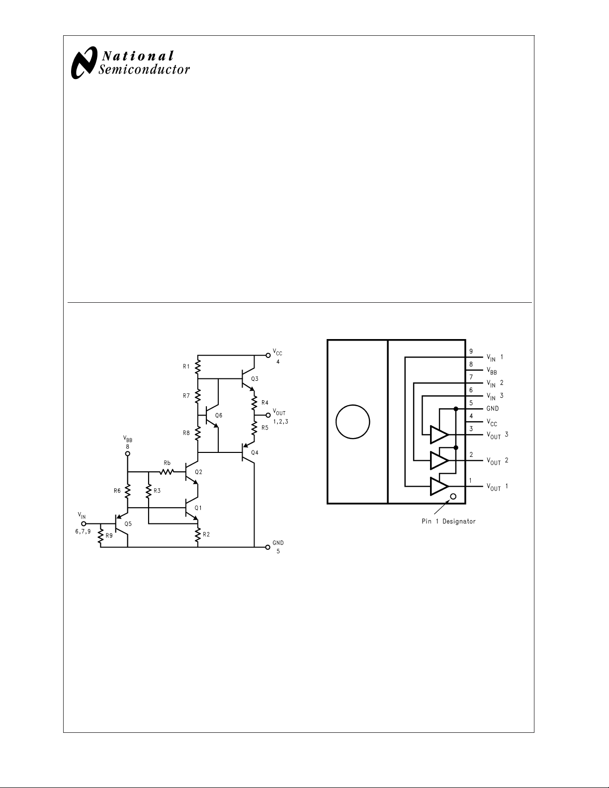
Schematic and Connection Diagrams
20082601
FIGURE 1. Simplified Schematic Diagram (One
Channel)
Top View
20082602
Order Number LM2460TA
See NS Package Number TA09A
© 2003 National Semiconductor Corporation DS200826 www.national.com
Absolute Maximum Ratings (Notes 1,
3)
LM2460
If Military/Aerospace specified devices are required,
please contact the National Semiconductor Sales Office/
Distributors for availability and specifications.
Supply Voltage (V
Bias Voltage (V
Input Voltage (V
Storage Temperature −40˚C to +150˚C
Lead Temperature
(Soldering,
) +136V
CC
) +16V
BB
) −0.5>V
IN
<
10 sec.) 265˚C
>
4.25V
IN
Junction Temperature (T
) 150˚C
J
Operating Ratings (Note 2)
V
CC
V
BB
V
IN
V
OUT
Case Temperature 100˚C
Do not operate the part without a heatsink
ESD Tolerance,
Human Body Model
Machine Model
2kV
200V
Electrical Characteristics
(See Figure 2 for Test Circuit) Unless otherwise noted: VCC= +120V, VBB= +8V, CL= 8 pF, TC= 50˚C
DC Tests: V
AC Tests: Output = 60 V
Symbol Parameter Conditions
I
CC
I
BB
V
OUT, 1
V
OUT, 2
A
V
∆A
V
LE Linearity Error (Note 4), (Note 5), No AC Input
t
(60 V
r
P-P
t
(60 V
f
P-P
t
(40 V
r
P-P
t
(40 V
f
P-P
OS Overshoot (Note 6) 5 %
Note 1: Absolute Maximum Ratings indicate limits beyond which damage to the device may occur.
Note 2: Operating Ratings indicate conditions for which the device is functional, but do not guarantee specific performance limits. For guaranteed specifications and
test conditions, see the Electrical Characteristics. Datasheet min/max specification limits are guaranteed by design, test, or statistical analysis. The guaranteed
specifications apply only for the test conditions listed. Some performance characteristics may change when the device is not operated under the listed test
conditions.
Note 3: All voltages are measured with respect to GND, unless otherwise specified.
Note 4: Calculated value from Voltage Gain test on each channel.
Note 5: Linearity Error is the variation in dc gain from V
Note 6: Input from signal generator: t
= +2.2 V
IN
DC
(45V − 105V) at 1 MHz
P-P
LM2460
Min Typ Max
Supply Current All Three Channels, No Video
Input, No Output Load
35 45 mA
Bias Current All Three Channels 15 25 mA
DC Output Voltage No AC Input Signal, VIN= 2.2
V
DC
DC Output Voltage No AC Input Signal, VIN= 1.2
V
DC
73 78 83 V
104 109 114 V
DC Voltage Gain No AC Input Signal −28 −32 −34 V/V
Gain Matching (Note 4), No AC Input Signal 1.0 dB
Signal
10 %
) Rise Time, 45V to 105V (Note 6), 10% to 90% 8.0 ns
) Fall Time, 45V to 105V (Note 6), 90% to 10% 11.5 ns
) Rise Time, 65V to 105V (Note 6), 10% to 90% 7.7 ns
) Fall Time, 65V to 105V (Note 6), 90% to 10% 9.5 ns
= 1.1V to VIN= 3.8V.
IN
r,tf
<
1 ns.
+80V to +125V
+6V to +10V
+1V to +5V
+25V to +115V
Units
DC
DC
www.national.com 2
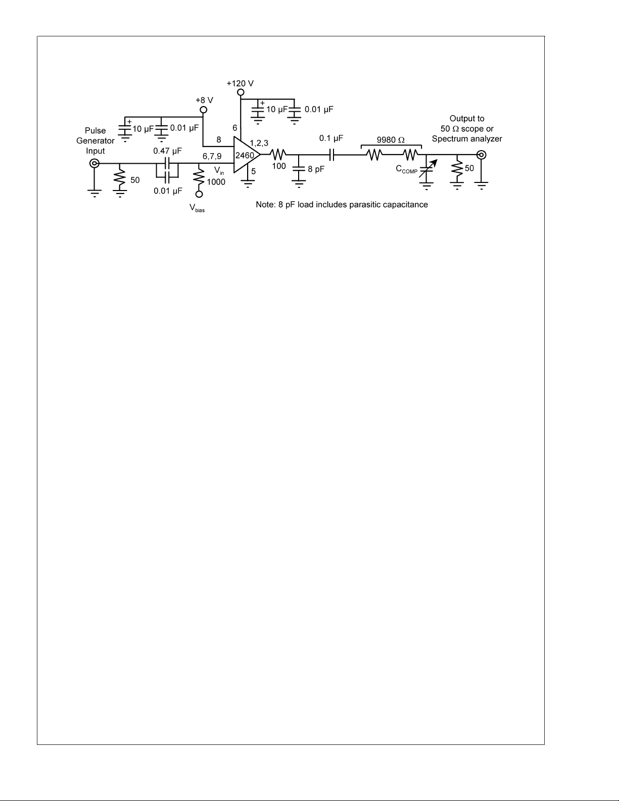
AC Test Circuit
20082615
FIGURE 2. Test Circuit (One Channel)
Figure 2 shows a typical test circuit for evaluation of the LM2460. This circuit is designed to allow testing of the LM2460 in a 50Ω
environment without the use of an expensive FET probe. The two 4990Ω resistors form a 200:1 divider with the 50Ω resistor and
the oscilloscope. A test point is included for easy use of an oscilloscope probe. The compensation capacitor is used to
compensate the stray capacitance of the two 4990Ω resistors to achieve flat frequency response.
LM2460
www.national.com3
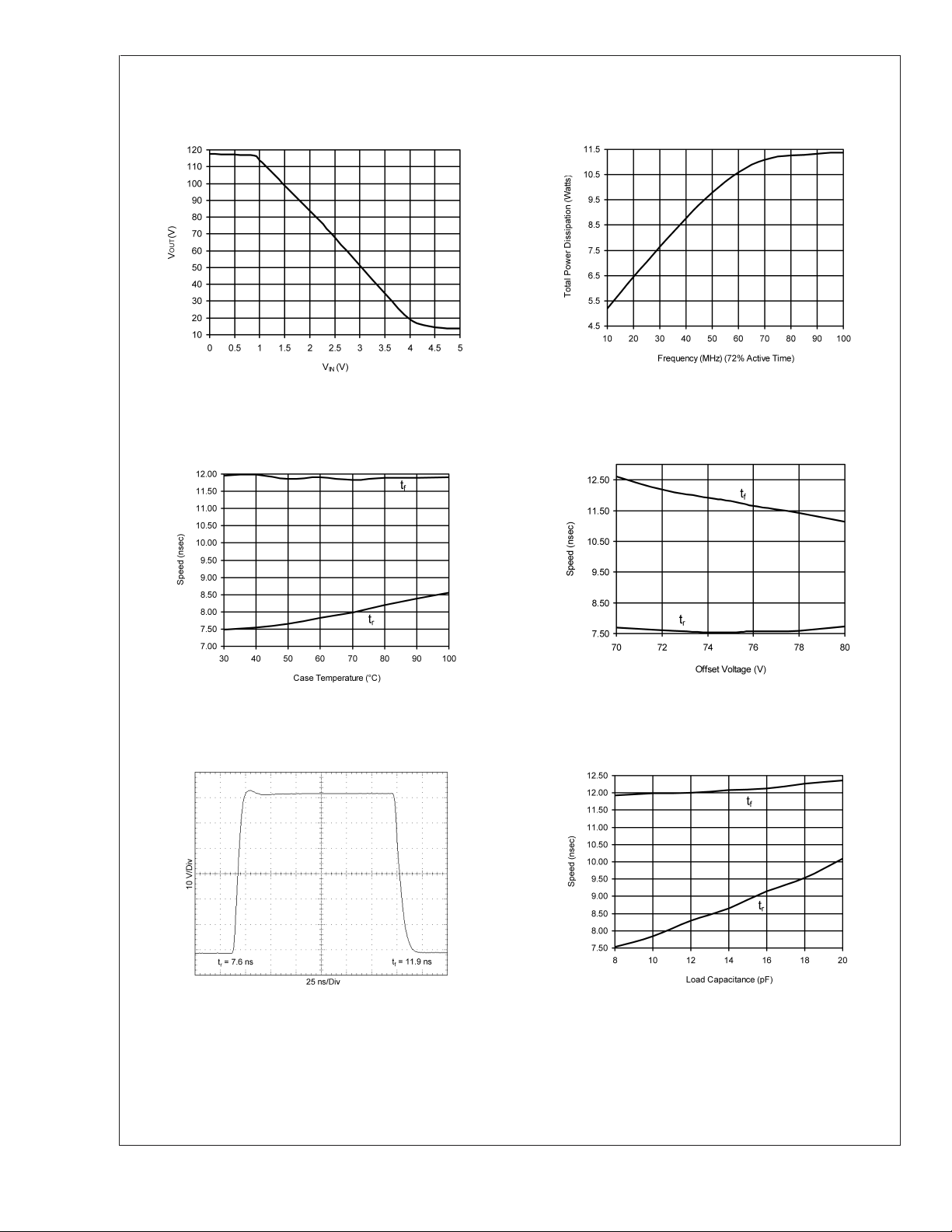
Typical Performance Characteristics (V
(45−105V), Test Circuit —Figure 2 unless otherwise specified.
LM2460
= +120 VDC,VBB=+8VDC,CL= 8 pF, V
CC
OUT
=60V
PP
FIGURE 3. VINvs V
OUT
FIGURE 4. Speed vs Case Temperature
20082603
20082604
20082606
FIGURE 6. Power Dissipation vs Frequency
20082607
FIGURE 7. Speed vs Offset Voltage
20082605
FIGURE 5. LM2460 Pulse Response
www.national.com 4
20082608
FIGURE 8. Speed vs Load Capacitance
 Loading...