

October 17, 2008
LM22670
3A SIMPLE SWITCHER®, Step-Down Voltage Regulator
with Synchronization or Adjustable Switching Frequency
LM22670 3A SIMPLE SWITCHER®, Step-Down Voltage Regulator with Synchronization or
Adjustable Switching Frequency
General Description
The LM22670 series of regulators are monolithic integrated
circuits which provide all of the active functions for a stepdown (buck) switching regulator capable of driving up to 3A
loads with excellent line and load regulation characteristics.
High efficiency (>90%) is obtained through the use of a low
ON-resistance N-channel MOSFET. The series consists of a
fixed 5V output and an adjustable version.
The SIMPLE SWITCHER® concept provides for an easy to
use complete design using a minimum number of external
components and National’s WEBENCH® design tool.
National’s WEBENCH® tool includes features such as external component calculation, electrical simulation, thermal simulation, and Build-It boards for easy design-in. The switching
clock frequency is provided by an internal fixed frequency oscillator which operates at 500 kHz. The switching frequency
can also be adjusted with an external resistor or synchronized
to an external clock up to 1MHz. It is also possible to selfsynchronize multiple regulators to share the same switching
frequency. The LM22670 series also has built in thermal shutdown, current limiting and an enable control input that can
power down the regulator to a low 25 µA quiescent current
standby condition.
Features
Wide input voltage range: 4.5V to 42V
■
Internally compensated voltage mode control
■
Stable with low ESR ceramic capacitors
■
120 mΩ N-channel MOSFET TO-263 THIN package
■
100 mΩ N-channel MOSFET PSOP-8 package
■
Output voltage options:
■
-ADJ (outputs as low as 1.285V)
-5.0 (output fixed to 5V)
±1.5% feedback reference accuracy
■
Switching frequency of 500 kHz, adjustable between 200
■
kHz and 1 MHz
-40°C to 125°C operating junction temperature range
■
Precision enable pin
■
Integrated boot diode
■
Integrated soft-start
■
Fully WEBENCH® enabled
■
Step-down and inverting buck-boost applications
■
Package
PSOP-8 (Exposed Pad)
■
TO-263 THIN (Exposed Pad)
■
Applications
Industrial Control
■
Telecom and Datacom Systems
■
Embedded Systems
■
Automotive Telematics and Body Electronics
■
Conversions from Standard 24V, 12V and 5V Input Rails
■
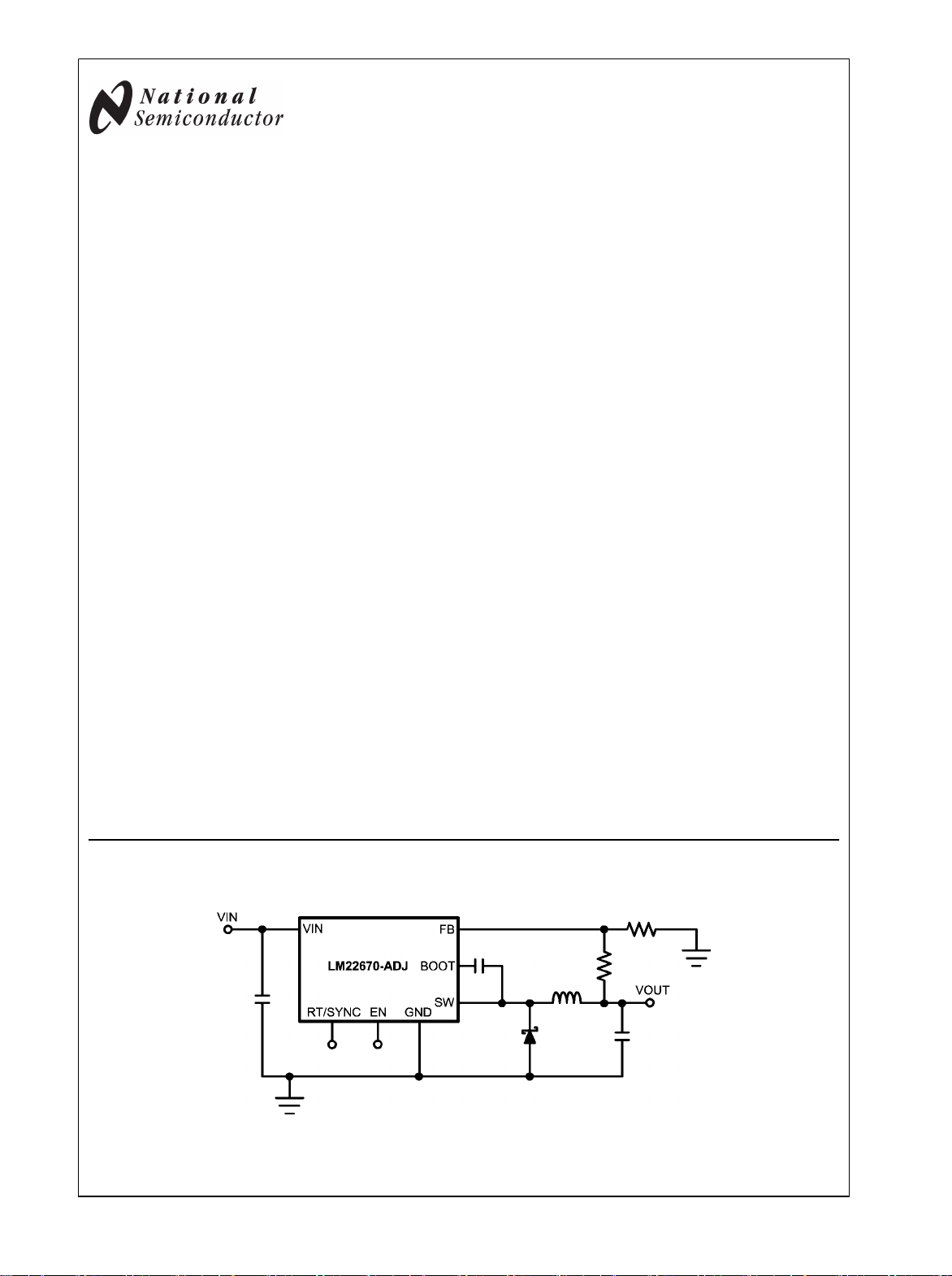
Simplified Application Schematic
30076001
© 2008 National Semiconductor Corporation 300760 www.national.com
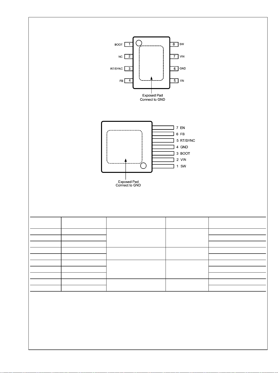
Connection Diagrams
LM22670
8-Lead Plastic PSOP-8 Package
NS Package Number MRA08B
7-Lead Plastic TO-263 THIN Package
NS Package Number TJ7A
30076040
30076002
Ordering Information
Output Voltage Order Number Package Type NSC Package
Drawing
ADJ LM22670MR-ADJ PSOP-8 Exposed Pad MRA08B 95 Units in Rails
ADJ LM22670MRE-ADJ 250 Units in Tape and Reel
ADJ LM22670MRX-ADJ 2500 Units in Tape and Reel
ADJ LM22670TJE-ADJ TO-263 THIN Exposed Pad TJ7A 250 Units in Tape and Reel
ADJ LM22670TJ-ADJ 1000 Units in Tape and Reel
5.0 LM22670MR-5.0 PSOP-8 Exposed Pad MRA08B 95 Units in Rails
5.0 LM22670MRE-5.0 250 Units in Tape and Reel
5.0 LM22670MRX-5.0 2500 Units in Tape and Reel
5.0 LM22670TJE-5.0 TO-263 THIN Exposed Pad TJ7A 250 Units in Tape and Reel
5.0 LM22670TJ-5.0 1000 Units in Tape and Reel
Supplied As
www.national.com 2
Pin Descriptions
LM22670
Pin Numbers
PSOP-8
Package
1 3 BOOT Bootstrap input Provides the gate voltage for the high side NFET.
2 - NC Not Connected Pin is not electrically connected inside the chip. Pin
3 5 RT/
4 6 FB Feedback pin Inverting input to the internal voltage error amplifier.
5 7 EN Precision enable pin When pulled low regulator turns off.
6 4 GND System ground Provide good capacitive decoupling between VIN and
7 2 VIN Source input voltage Input to the regulator. Operates from 4.5V to 42V.
8 1 SW Switch pin Attaches to the switch node.
Pin Numbers
TO-263 THIN
Package
Name Description Application Information
does function as thermal conductor.
SYNC
Oscillator frequency adjust pin or
frequency synchronization
A resistor connected from this pin to GND adjusts the
oscillator frequency. This pin can also accept an input
for synchronization from an external clock. Pin can be
left floating and internal setting will be default to 500
kHz.
this pin.
3 www.national.com
Absolute Maximum Ratings (Note 1)
If Military/Aerospace specified devices are required,
LM22670
please contact the National Semiconductor Sales Office/
Distributors for availability and specifications.
VIN to GND 43V
EN Pin Voltage -0.5V to 6V
RT/SYNC Pin Voltage -0.5V to 7V
SW to GND (Note 2) -5V to V
BOOT Pin Voltage VSW + 7V
FB Pin Voltage -0.5V to 7V
Power Dissipation Internally Limited
Junction Temperature 150°C
Soldering Information
Vapor Phase (75 sec.) 219°C
Infrared (10 sec.) 240°C
Wave (4 sec.) 260°C
ESD Rating (Note 3)
Human Body Model ±2 kV
Storage Temperature Range -65°C to +150°C
IN
Operating Ratings (Note 1)
Supply Voltage (VIN)
4.5V to 42V
Junction Temperature Range -40°C to +125°C
Electrical Characteristics Limits in standard type are for T
= 25°C only; limits in boldface type apply over the
J
junction temperature (TJ) range of -40°C to +125°C. Minimum and Maximum limits are guaranteed through test, design, or statistical
correlation. Typical values represent the most likely parametric norm at TA = TJ = 25°C, and are provided for reference purposes
only. Unless otherwise specified: VIN = 12V.
Symbol Parameter Conditions Min
(Note 5)
Typ
(Note 4)
Max
(Note 5)
LM22670-5.0
V
FB
Feedback Voltage VIN = 8V to 42V 4.925/4.9 5.0 5.075/5.1 V
LM22670-ADJ
V
FB
Feedback Voltage VIN = 4.7V to 42V 1.266/1.259 1.285 1.304/1.311 V
All Output Voltage Versions
I
I
STDBY
I
CL
I
Q
L
Quiescent Current VFB = 5V 3.4 6 mA
Standby Quiescent Current EN Pin = 0V 25 40 µA
Current Limit 3.4/3.35 4.2 5.3/5.5 A
Output Leakage Current VIN = 42V, EN Pin = 0V, VSW = 0V 0.2 2 µA
VSW = -1V 0.1 3 µA
R
DS(ON)
Switch On-Resistance TO-263 THIN Package 0.12 0.16/0.22
PSOP-8 Package 0.10 0.16/0.20
f
T
OFFMIN
T
ONMIN
I
BIAS
V
I
EN
F
SYNC
V
SYNC
O
EN
Oscillator Frequency 400 500 600 kHz
Minimum Off-time 300 ns
Minimum On-time 100 ns
Feedback Bias Current VFB = 1.3V (ADJ Version Only) 230 nA
Enable Threshold Voltage 1.3 1.6 1.9 V
Enable Input Current EN Input = 0V 6 µA
Synchronization Frequency V
Synchronization Threshold
= 3.5V, 50% duty-cycle 1 MHz
SYNC
1.75 V
Voltage
T
SD
Thermal Shutdown
150 °C
Threshold
θ
JA
Thermal Resistance TJ Package, Junction to ambient
22 °C/W
temperature resistance (Note 6)
θ
JA
Thermal Resistance MR Package, Junction to ambient
60 °C/W
temperature resistance (Note 7)
Units
Ω
www.national.com 4
Note 1: Absolute Maximum Ratings indicate limits beyond which damage to the device may occur, including inoperability and degradation of device reliability
and/or performance. Functional operation of the device and/or non-degradation at the Absolute Maximum Ratings or other conditions beyond those indicated in
the recommended Operating Ratings is not implied. The recommended Operating Ratings indicate conditions at which the device is functional and should not be
operated beyond such conditions.
Note 2: The absolute maximum specification of the ‘SW to GND’ applies to DC voltage. An extended negative voltage limit of -10V applies to a pulse of up to 50
ns.
Note 3: ESD was applied using the human body model, a 100 pF capacitor discharged through a 1.5 kΩ resistor into each pin.
Note 4: Typical values represent most likely parametric norms at the conditions specified and are not guaranteed.
Note 5: Min and Max limits are 100% production tested at 25°C. Limits over the operating temperature range are guaranteed through correlation using Statistical
Quality Control (SQC) methods. Limits are used to calculate National’s Average Outgoing Quality Level (AOQL).
Note 6: The value of θJA for the TO-263 THIN (TJ) package of 22°C/W is valid if package is mounted to 1 square inch of copper. The θJA value can range from
20 to 30°C/W depending on the amount of PCB copper dedicated to heat transfer. See application note AN-1797 for more information.
Note 7: The value of θJA for the PSOP-8 exposed pad (MR) package of 60°C/W is valid if package is mounted to 1 square inch of copper. The θJA value can
range from 42 to 115°C/W depending on the amount of PCB copper dedicated to heat transfer.
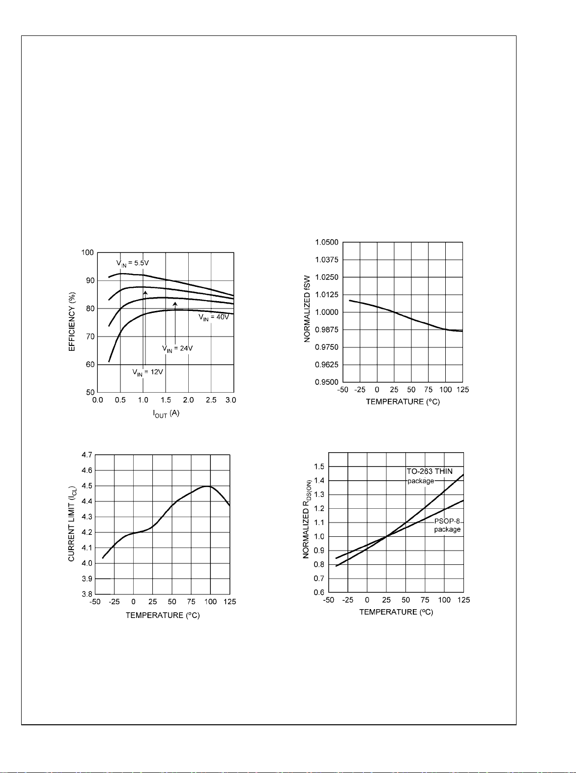
Typical Performance Characteristics Unless otherwise specified the following conditions apply: Vin =
12V, TJ = 25°C.
LM22670
Efficiency vs I
V
OUT
OUT
= 3.3V
and V
IN
Current Limit vs Temperature
30076027
Normalized Switching Frequency vs Temperature
30076004
Normalized R
vs Temperature
DS(ON)
30076003
30076008
5 www.national.com
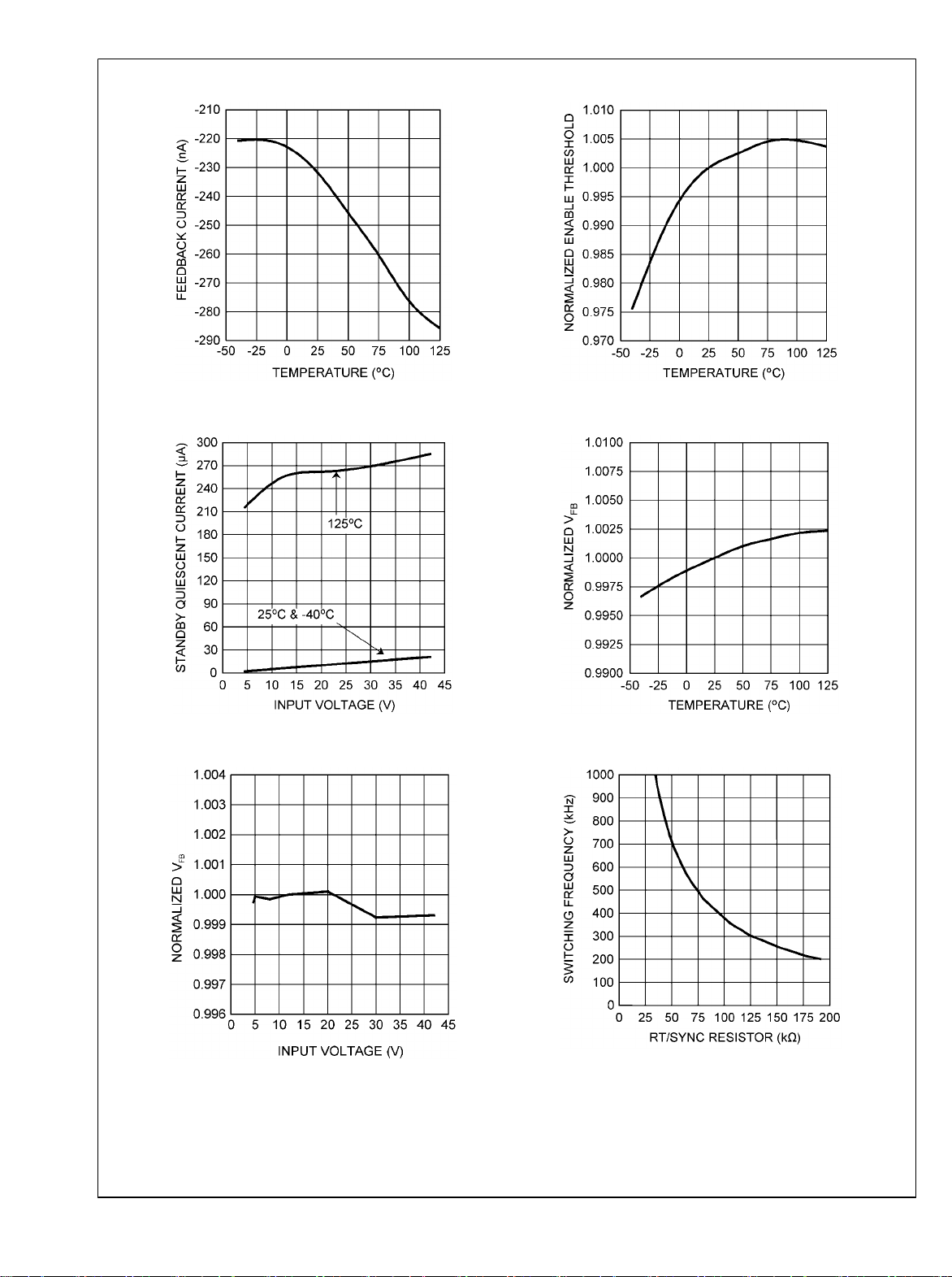
LM22670
Feedback Bias Current vs Temperature
Normalized Enable Threshold Voltage vs Temperature
30076005
Standby Quiescent Current vs Input Voltage
30076006
Normalized Feedback Voltage vs Input Voltage
30076010
Normalized Feedback Voltage vs Temperature
30076007
Switching Frequency vs RT/SYNC Resistor
30076009
www.national.com 6
30076013

Typical Application Circuit and Block Diagram
LM22670
FIGURE 1. 3.3V V
, 3A at 600 kHz
OUT
30076014
7 www.national.com

Detailed Operating Description
The LM22670 switching regulator features all of the functions
LM22670
necessary to implement an efficient high voltage buck regulator using a minimum of external components. This easy to
use regulator integrates a 42V N-Channel switch with an output current capability of 3A. The regulator control method is
based on voltage mode control with input voltage feed forward. The loop compensation is integrated into the LM22670
so that no external compensation components need to be selected or utilized. Voltage mode control offers short minimum
on-times allowing short duty-cycles necessary in high input
voltage applications. The operating frequency is fixed at
500kHz to allow for small external components while avoiding
excessive switching losses. The switching frequency can be
adjusted with an external resistor from 200 kHz to 1 MHz or
it can be synchronized to an external clock up to 1 MHz. The
output voltage can be set as low as 1.285V with the -ADJ
device. Fault protection features include current limiting, thermal shutdown and remote shutdown capability. The device is
available in the TO-263 THIN and PSOP-8 packages featuring an exposed pad to aid thermal dissipation.
The functional block diagram with typical application of the
LM22670 are shown in Figure 1.
The internal compensation of the -ADJ option of the LM22670
is optimized for output voltages up to 5V. If an output voltage
of 5V or higher is needed, the -5.0 fixed output voltage option
with an additional external resistive feedback voltage divider
may also be used.
Precision Enable
The precision enable pin (EN) can be used to shut down the
power supply. Connecting this pin to ground or to a voltage
less than typical 1.6V will completely turn off the regulator.
The current drain from the input supply when off is typically
25 µA with 12V input voltage. The power consumed during
this off state is mostly defined by an internal 2 MΩ resistor to
VIN. The enable pin has an internal pull-up current source of
approximately 6 µA. When driving the enable pin, the high
voltage level for the on condition should not exceed the 6V
absolute maximum limit. When enable control is not required,
the EN pin should be left floating. The precision feature enables simple sequencing of multiple power supplies with a
resistor divider from another power supply.
Maximum Duty-Cycle / Dropout Voltage
The typical maximum duty-cycle is 85% at 500 kHz switching
frequency. This corresponds to a typical minimum off-time of
300 ns. When operating at switching frequencies higher than
500 kHz, the 300 ns minimum off-time results in a lower maximum duty-cycle limit than 85%. This forced off-time is important to provide enough time for the Cboot capacitor to charge
during each cycle.
The lowest input voltage required to maintain operation is:
Where VD is the forward voltage drop across the re-circulating
Schottky diode and VQ is the voltage drop across the internal
power N-FET of the LM22670. The R
specified in the electrical characteristics section of this
of the FET is
DS(ON)
datasheet to calculate VQ according to the FET current. F is
the switching frequency.
Minimum Duty-Cycle
Besides a minimum off-time, there is also a minimum on-time
which will take effect when the output voltage is adjusted very
low and the input voltage is very high. Should the operation
require a shorter minimum on-time than the typical 100 ns,
individual switching pulses will be skipped.
where D is the duty-cycle.
Current Limit
When the power switch turns on, the slight capacitance loading of the Schottky diode, D1, causes a leading-edge current
spike with an extended ringing period. This spike can cause
the current limit comparator to trip prematurely. A leading
edge blanking time (T
sampling the spike.
When the switch current reaches the current limit threshold,
the switch is immediately turned off and the internal switching
frequency is reduced. This extends the off time of the switch
to prevent a steady state high current condition. As the switch
current falls below the current limit threshold, the switch current will attempt to turn on. If a load fault continues, the switch
will again exceed the threshold and turn off. This will result in
a low duty-cycle pulsing of the power switch to minimize the
overall fault condition power dissipation.
The switching frequency will reduce (fold back) if the overload
condition causes the output voltage to be 72.4% (typical) of
the adjusted output voltage.
The current limit will only protect the inductor from a runaway
condition if the LM22670 is operating in its safe operating
area. A runaway condition of the inductor is potentially catastrophic to the application. For every design, the safe operating
area needs to be calculated. Factors in determining the safe
operating area are the switching frequency, input voltage,
output voltage, minimum on-time and feedback voltage during an over current condition.
As a first pass check, if the following equation holds true, a
given design is considered in a safe operating area and the
current limit will protect the circuit:
VIN x T
If the equation above does not hold true, the following secondary equation will need to hold true to be in safe operating
area:
If both equations do not hold true, a particular design will not
have an effective current limit function which might damage
the circuit during startup, over current conditions, or steady
state over current and short circuit condition. Oftentimes a
reduction of the maximum input voltage or a reduction of the
switching frequency will bring a design into the safe operating
area.
When synchronized to an external sync pulse, the LM22670
will not fold back the switching frequency in an over current
condition.
) of 110 ns (typical) is used to avoid
BLK
BLK
x F < V
OUT
x 0.724
www.national.com 8

LM22670
Soft-Start
The soft-start feature allows the regulator to gradually reach
the initial steady state operating point, thus reducing start-up
stresses and surges. The soft-start is fixed to 500 µs (typical)
start-up time and cannot be modified.
Switching Frequency Setting and Synchronization
There are three different modes for the RT/SYNC pin. It can
be left floating for a 500 kHz switching frequency.
A resistor from the RT/SYNC pin to ground can be used to
adjust the switching frequency between 200 kHz and 1 MHz.
An external synchronization pulse can be applied to the RT/
SYNC pin for switching frequencies up to 1 MHz. The
LM22670 internally sets the RT/SYNC mode during start up.
Many applications are limited to lower switching frequencies
due to minimum on-time and minimum off-time requirements
as well as increased switching losses at switching frequencies higher than 500 kHz. In case of synchronizing to an
external sync pulse, the clock pulse must be in a valid low or
high state when the LM22670 starts up and can be applied
after device regulation. The internal oscillator will synchronize
to the external sync pulse rising edge. If the external sync
pulse is disconnected the LM22670 switching frequency will
return to default 500 kHz (typ.).
When operating at frequencies above 500 kHz, external components such as the inductor and the output capacitors cannot be reduced dramatically. This is due to the fixed internal
compensation and stability requirements. Running the
LM22670 at frequencies higher than 500 kHz is intended for
applications with EMI or beat frequency concerns. The flexibility of increasing the switching frequency above 500 kHz can
be used to operate outside a critical signal frequency band of
an application. This can also be used to set multiple switchers
in an application to the same frequency to reduce beat frequencies and simplify filtering.
See the current limit section of this datasheet for information
about the safe operating area. When synchronizing to an external synchronization pulse, the LM22670 will not fold back
the switching frequency in an over current condition.
The typical curve below shows adjusted switching frequencies with different frequency set resistors from the RT/SYNC
pin to ground.
Self Synchronize
It is also possible to self-synchronize multiple LM22670 regulators to share the same switching frequency. This can be
done by attaching the RT/SYNC pins together and putting a
1 kΩ resistor to ground. The diagram in Figure 3 illustrates
this setup. The two regulators will be clocked at the same frequency but slightly phase shifted according to the minimum
off-time of the regulator with the fastest running oscillator. The
slight phase shift helps to reduce the stress on the input capacitors of the power supply.
30076030
FIGURE 3. Self Synchronizing Setup
Boot Pin
The LM22670 integrates an N-Channel FET switch and associated floating high voltage level shift / gate driver. This gate
driver circuit works in conjunction with an internal diode and
an external bootstrap capacitor. A 0.01 µF ceramic capacitor
connected with short traces between the BOOT pin and the
SW pin is recommended to effectively drive the internal FET
switch. During the off-time of the switch, the SW voltage is
approximately -0.5V and the external bootstrap capacitor is
charged from the internal supply through the internal bootstrap diode. When operating with a high PWM duty-cycle, the
buck switch will be forced off each cycle to ensure that the
bootstrap capacitor is recharged. See the maximum duty-cycle section for more details.
Thermal Protection
Internal Thermal Shutdown circuitry protects the LM22670 in
the event the maximum junction temperature is exceeded.
When activated, typically at 150°C, the regulator is forced into
a low power reset state. There is a typical hysteresis of 15
degrees.
30076013
FIGURE 2. Switching Frequency vs RT/SYNC Resistor
Internal Compensation
The LM22670 has internal compensation designed for a stable loop with a wide range of external power stage components.
Insuring stability of a design with a specific power stage (inductor and output capacitor) can be tricky. The LM22670
stability can be verified over varying loads and input and output voltages using WEBENCH® Designer online circuit simulation tool at www.national.com. A quick start spreadsheet
can also be downloaded from the online product folder.
The internal compensation of the -ADJ option of the LM22670
is optimized for output voltages below 5V. If an output voltage
9 www.national.com

of 5V or higher is needed, the -5.0 option with an additional
external resistor divider may also be used.
The typical location of the internal compensation poles and
LM22670
zeros as well as the DC gain is given in Table 1. The LM22670
has internal type III compensation allowing for the use of most
output capacitors including ceramics.
This information can be used to calculate the transfer function
from the FB pin to the internal compensation node (input to
the PWM comparator in the block diagram).
TABLE 1.
Corners Frequency
Pole 1 150 kHz
Pole 2 250 kHz
Pole 3 100 Hz
Zero 1 1.5 kHz
Zero 2 15 kHz
DC gain 37.5 dB
For the power stage transfer function the standard voltage
mode formulas for the double pole and the ESR zero apply:
The peak ramp level of the oscillator signal feeding into the
PWM comparator is VIN/10 which equals a gain of 20dB of
this modulator stage of the IC. The -5.0 fixed output voltage
option has twice the gain of the compensation transfer function compared to the -ADJ option which is 43.5 dB instead of
37.5 dB.
Generally, calculation as well as simulation can only aid in
selecting good power stage components. A good design practice is to test for stability with load transient tests or loop
measurement tests. Application note AN-1889 shows how to
easily perform a loop transfer function measurement with only
an oscilloscope and a function generator.
Application Information
EXTERNAL COMPONENTS
The following design procedures can be used to design a nonsynchronous buck converter with the LM22670.
Inductor
The inductor value is determined based on the load current,
ripple current, and the minimum and maximum input voltage.
To keep the application in continuous current conduction
mode (CCM), the maximum ripple current, I
less than twice the minimum load current.
The general rule of keeping the inductor current peak-to-peak
ripple around 30% of the nominal output current is a good
compromise between excessive output voltage ripple and excessive component size and cost. When selecting the inductor ripple current ensure that the peak current is below the
minimum current limit as given in the Electrical Characteristics section. Using this value of ripple current, the value of
inductor, L, is calculated using the following formula:
RIPPLE
, should be
where F is the switching frequency which is 500 kHz without
an external frequency set resistor or external sync signal applied to the RT/SYNC pin. If the switching frequency is set
higher than 500kHz, the inductance value may not be reduced
accordingly due to stability requirements. The internal compensation is optimized for circuits with a 500 kHz switching
frequency. See the internal compensation section for more
details. This procedure provides a guide to select the value of
the inductor L. The nearest standard value will then be used
in the circuit.
Increasing the inductance will generally slow down the transient response but reduce the output voltage ripple amplitude.
Reducing the inductance will generally improve the transient
response but increase the output voltage ripple.
The inductor must be rated for the peak current, I
vent saturation. During normal loading conditions, the peak
PK+
, to pre-
current occurs at maximum load current plus maximum ripple.
Under an overload condition as well as during load transients,
the peak current is limited to 4.2A typical (5.5A maximum).
This requires that the inductor be selected such that it can run
at the maximum current limit and not only the steady state
current.
Depending on inductor manufacturer, the saturation rating is
defined as the current necessary for the inductance to reduce
by 30% at 20°C. In typical designs the inductor will run at
higher temperatures. If the inductor is not rated for enough
current, it might saturate and due to the propagation delay of
the current limit circuitry, the power supply may get damaged.
Input Capacitor
Good quality input capacitors are necessary to limit the ripple
voltage at the VIN pin while supplying most of the switch current during on-time. When the switch turns on, the current into
the VIN pin steps to the peak value, then drops to zero at turnoff. The average current into VIN during switch on-time is the
load current. The input capacitance should be selected for
RMS current, I
proximation for the required ripple current rating necessary is
I
> I
RMS
OUT
, and minimum ripple voltage. A good ap-
RMS
/ 2.
Quality ceramic capacitors with a low ESR should be selected
for the input filter. To allow for capacitor tolerances and voltage effects, multiple capacitors may be used in parallel. If step
input voltage transients are expected near the maximum rating of the LM22670, a careful evaluation of ringing and possible voltage spikes at the VIN pin should be completed. An
additional damping network or input voltage clamp may be
required in these cases.
Usually putting a higher ESR electrolytic input capacitor in
parallel to the low ESR bypass capacitor will help to reduce
excessive voltages during a line transient and will also move
the resonance frequency of the input filter away from the regulator bandwidth.
Output Capacitor
The output capacitor can limit the output ripple voltage and
provide a source of charge for transient loading conditions.
Multiple capacitors can be placed in parallel. Very low ESR
capacitors such as ceramic capacitors reduce the output ripple voltage and noise spikes, while larger higher ESR capacitors in parallel provide large bulk capacitance for transient
loading conditions. An approximation for the output voltage
ripple is:
www.national.com 10

where ΔIL is the inductor ripple current.
If the switching frequency is set higher than 500 kHz, the ca-
pacitance value may not be reduced accordingly due to stability requirements. The internal compensation is optimized
for circuits with a 500 kHz switching frequency. See the internal compensation section for more details.
LM22670
Cboot Capacitor
The bootstrap capacitor between the BOOT pin and the SW
pin supplies the gate current to turn on the N-channel MOSFET. The recommended value of this capacitor is 10 nF and
should be a good quality, low ESR ceramic capacitor.
It is possible to put a small resistor in series with the Cboot
capacitor to slow down the turn-on transition time of the internal N-channel MOSFET. Resistors in the range of 10Ω to
50Ω can slow down the transition time. This can reduce EMI
of a switched mode power supply circuit. Using such a series
resistor is not recommended for every design since it will increase the switching losses of the application and makes
thermal considerations more challenging.
Resistor Divider
For the -5.0 option no resistor divider is required for 5V output
voltage. The output voltage should be directly connected to
the FB pin. Output voltages above 5V can use the -5.0 option
with a resistor divider as an alternative to the -ADJ option.
This may offer improved loop bandwidth in some applications.
See the Internal Compensation section for more details.
For the -ADJ option no resistor divider is required for 1.285V
output voltage. The output voltage should be directly connected to the FB pin. Other output voltages can use the -ADJ
option with a resistor divider.
The resistor values can be determined by the following equations:
-ADJ option:
-5.0 option:
Where VFB = 1.285V typical for the -ADJ option and 5V for the
-5.0 option
30076023
FIGURE 4. Resistive Feedback Divider
A maximum value of 10 kΩ is recommended for the sum of
R1 and R2 to keep high output voltage accuracy for the –ADJ
option. A maximum of 2 kΩ is recommended for the -5.0 output voltage option. For the 5V fixed output voltage option, the
total internal divider resistance is typically 9.93 kΩ.
At loads less than 5 mA, the boot capacitor will not hold
enough charge to power the internal high side driver. The
output voltage may droop until the boot capacitor is
recharged. Selecting a total feedback resistance to be below
3 kΩ will provide some minimal load and can keep the output
voltage from collapsing in such low load conditions.
Catch Diode
A Schottky type re-circulating diode is required for all
LM22670 applications. Ultra-fast diodes which are not Schottky diodes are not recommended and may result in damage
to the IC due to reverse recovery current transients. The near
ideal reverse recovery characteristics and low forward voltage drop of Schottky diodes are particularly important diode
characteristics for high input voltage and low output voltage
applications common to the LM22670. The reverse recovery
characteristic determines how long the current surge lasts
each cycle when the N-channel MOSFET is turned on. The
reverse recovery characteristics of Schottky diodes minimizes the peak instantaneous power in the switch occurring
during turn-on for each cycle. The resulting switching losses
are significantly reduced when using a Schottky diode. The
reverse breakdown rating should be selected for the maximum VIN, plus some safety margin. A rule of thumb is to select
a diode with the reverse voltage rating of 1.3 times the maximum input voltage.
The forward voltage drop has a significant impact on the conversion efficiency, especially for applications with a low output
voltage. ‘Rated’ current for diodes varies widely from various
manufacturers. The worst case is to assume a short circuit
load condition. In this case the diode will carry the output current almost continuously. For the LM22670 this current can
be as high as 4.2A (typical). Assuming a worst case 1V drop
across the diode, the maximum diode power dissipation can
be as high as 4.2W.
11 www.national.com

Circuit Board Layout
Board layout is critical for switching power supplies. First, the
LM22670
ground plane area must be sufficient for thermal dissipation
purposes. Second, appropriate guidelines must be followed
to reduce the effects of switching noise. Switch mode converters are very fast switching devices. In such devices, the
rapid increase of input current combined with the parasitic
trace inductance generates unwanted L di/dt noise spikes.
The magnitude of this noise tends to increase as the output
current increases. This parasitic spike noise may turn into
electromagnetic interference (EMI) and can also cause problems in device performance. Therefore, care must be taken
in layout to minimize the effect of this switching noise.
The most important layout rule is to keep the AC current loops
as small as possible. Figure 5 shows the current flow of a buck
converter. The top schematic shows a dotted line which represents the current flow during the FET switch on-state. The
middle schematic shows the current flow during the FET
switch off-state.
The bottom schematic shows the currents referred to as AC
currents. These AC currents are the most critical since current
is changing in very short time periods. The dotted lines of the
bottom schematic are the traces to keep as short as possible.
This will also yield a small loop area reducing the loop inductance. To avoid functional problems due to layout, review the
PCB layout example. Providing 3A of output current in a very
low thermal resistance package such as the TO-263 THIN is
challenging considering the trace inductances involved. Best
results are achieved if the placement of the LM22670, the bypass capacitor, the Schottky diode and the inductor are
placed as shown in the example. It is also recommended to
use 2oz copper boards or thicker to help thermal dissipation
and to reduce the parasitic inductances of board traces.
It is very important to ensure that the exposed DAP on the
TO-263 THIN package is soldered to the ground area of the
PCB to reduce the AC trace length between the bypass capacitor ground and the ground connection to the LM22670.
Not soldering the DAP to the board may result in erroneous
operation due to excessive noise on the board.
Thermal Considerations
The two highest power dissipating components are the recirculating diode and the LM22670 regulator IC. The easiest
method to determine the power dissipation within the
LM22670 is to measure the total conversion losses (Pin –
Pout) then subtract the power losses in the Schottky diode
and output inductor. An approximation for the Schottky diode
loss is:
P = (1 - D) x I
An approximation for the output inductor power is:
P = I
OUT
where R is the DC resistance of the inductor and the 1.1 factor
is an approximation for the AC losses. The regulator has an
exposed thermal pad to aid power dissipation. Adding several
vias under the device to the ground plane will greatly reduce
the regulator junction temperature. Selecting a diode with an
exposed pad will aid the power dissipation of the diode. The
most significant variables that affect the power dissipated by
the LM22670 are the output current, input voltage and operating frequency. The power dissipated while operating near
the maximum output current and maximum input voltage can
be appreciable. The junction-to-ambient thermal resistance of
the LM22670 will vary with the application. The most significant variables are the area of copper in the PC board, the
number of vias under the IC exposed pad and the amount of
forced air cooling provided. The integrity of the solder connection from the IC exposed pad to the PC board is critical.
Excessive voids will greatly diminish the thermal dissipation
capacity. The junction-to-ambient thermal resistance of the
LM22670 TO-263 THIN and PSOP-8 packages are specified
in the Electrical Characteristics table under the applicable
conditions. For more information regarding the TO-263 THIN
package, refer to Application Note AN-1797 at
www.national.com.
OUT
2
x R x 1.1,
x V
D
30076024
FIGURE 5. Current Flow in a Buck Application
www.national.com 12

PCB Layout Example for TO-263 THIN Package
LM22670
30076025
13 www.national.com

PCB Layout Example for PSOP-8 Package
LM22670
www.national.com 14
30076041

Schematic for Buck/Boost (Inverting) Application
See AN-1888 for more information on the inverting (buckboost) application generating a negative output voltage from
a positive input voltage.
LM22670
30076026
15 www.national.com

Physical Dimensions inches (millimeters) unless otherwise noted
LM22670
7-Lead Plastic TO-263 THIN Package
NS Package Number TJ7A
8-Lead PSOP Package
NS Package Number MRA08B
www.national.com 16

Notes
LM22670
17 www.national.com

Notes
For more National Semiconductor product information and proven design tools, visit the following Web sites at:
Products Design Support
Amplifiers www.national.com/amplifiers WEBENCH www.national.com/webench
Audio www.national.com/audio Analog University www.national.com/AU
Clock Conditioners www.national.com/timing App Notes www.national.com/appnotes
Data Converters www.national.com/adc Distributors www.national.com/contacts
Displays www.national.com/displays Green Compliance www.national.com/quality/green
Ethernet www.national.com/ethernet Packaging www.national.com/packaging
Interface www.national.com/interface Quality and Reliability www.national.com/quality
LVDS www.national.com/lvds Reference Designs www.national.com/refdesigns
Power Management www.national.com/power Feedback www.national.com/feedback
Adjustable Switching Frequency
Switching Regulators www.national.com/switchers
LDOs www.national.com/ldo
LED Lighting www.national.com/led
PowerWise www.national.com/powerwise
Serial Digital Interface (SDI) www.national.com/sdi
Temperature Sensors www.national.com/tempsensors
Wireless (PLL/VCO) www.national.com/wireless
THE CONTENTS OF THIS DOCUMENT ARE PROVIDED IN CONNECTION WITH NATIONAL SEMICONDUCTOR CORPORATION
(“NATIONAL”) PRODUCTS. NATIONAL MAKES NO REPRESENTATIONS OR WARRANTIES WITH RESPECT TO THE ACCURACY
OR COMPLETENESS OF THE CONTENTS OF THIS PUBLICATION AND RESERVES THE RIGHT TO MAKE CHANGES TO
SPECIFICATIONS AND PRODUCT DESCRIPTIONS AT ANY TIME WITHOUT NOTICE. NO LICENSE, WHETHER EXPRESS,
IMPLIED, ARISING BY ESTOPPEL OR OTHERWISE, TO ANY INTELLECTUAL PROPERTY RIGHTS IS GRANTED BY THIS
DOCUMENT.
TESTING AND OTHER QUALITY CONTROLS ARE USED TO THE EXTENT NATIONAL DEEMS NECESSARY TO SUPPORT
NATIONAL’S PRODUCT WARRANTY. EXCEPT WHERE MANDATED BY GOVERNMENT REQUIREMENTS, TESTING OF ALL
PARAMETERS OF EACH PRODUCT IS NOT NECESSARILY PERFORMED. NATIONAL ASSUMES NO LIABILITY FOR
APPLICATIONS ASSISTANCE OR BUYER PRODUCT DESIGN. BUYERS ARE RESPONSIBLE FOR THEIR PRODUCTS AND
APPLICATIONS USING NATIONAL COMPONENTS. PRIOR TO USING OR DISTRIBUTING ANY PRODUCTS THAT INCLUDE
NATIONAL COMPONENTS, BUYERS SHOULD PROVIDE ADEQUATE DESIGN, TESTING AND OPERATING SAFEGUARDS.
EXCEPT AS PROVIDED IN NATIONAL’S TERMS AND CONDITIONS OF SALE FOR SUCH PRODUCTS, NATIONAL ASSUMES NO
LIABILITY WHATSOEVER, AND NATIONAL DISCLAIMS ANY EXPRESS OR IMPLIED WARRANTY RELATING TO THE SALE
AND/OR USE OF NATIONAL PRODUCTS INCLUDING LIABILITY OR WARRANTIES RELATING TO FITNESS FOR A PARTICULAR
PURPOSE, MERCHANTABILITY, OR INFRINGEMENT OF ANY PATENT, COPYRIGHT OR OTHER INTELLECTUAL PROPERTY
RIGHT.
LIFE SUPPORT POLICY
NATIONAL’S PRODUCTS ARE NOT AUTHORIZED FOR USE AS CRITICAL COMPONENTS IN LIFE SUPPORT DEVICES OR
SYSTEMS WITHOUT THE EXPRESS PRIOR WRITTEN APPROVAL OF THE CHIEF EXECUTIVE OFFICER AND GENERAL
COUNSEL OF NATIONAL SEMICONDUCTOR CORPORATION. As used herein:
Life support devices or systems are devices which (a) are intended for surgical implant into the body, or (b) support or sustain life and
whose failure to perform when properly used in accordance with instructions for use provided in the labeling can be reasonably expected
to result in a significant injury to the user. A critical component is any component in a life support device or system whose failure to perform
can be reasonably expected to cause the failure of the life support device or system or to affect its safety or effectiveness.
National Semiconductor and the National Semiconductor logo are registered trademarks of National Semiconductor Corporation. All other
brand or product names may be trademarks or registered trademarks of their respective holders.
Copyright© 2008 National Semiconductor Corporation
For the most current product information visit us at www.national.com
LM22670 3A SIMPLE SWITCHER®, Step-Down Voltage Regulator with Synchronization or
www.national.com
National Semiconductor
Americas Technical
Support Center
Email: support@nsc.com
Tel: 1-800-272-9959
National Semiconductor Europe
Technical Support Center
Email: europe.support@nsc.com
German Tel: +49 (0) 180 5010 771
English Tel: +44 (0) 870 850 4288
National Semiconductor Asia
Pacific Technical Support Center
Email: ap.support@nsc.com
National Semiconductor Japan
Technical Support Center
Email: jpn.feedback@nsc.com
 Loading...