

June 2, 2008
LM20323
36V, 3A PowerWise® 500 kHz Synchronous Buck Regulator
LM20323 36V, 3A PowerWise
General Description
The LM20323 is a full featured 500kHz synchronous buck
regulator capable of delivering up to 3A of load current. The
current mode control loop is externally compensated with only
two components, offering both high performance and ease of
use. The device is optimized to work over the input voltage
range of 4.5V to 36V making it well suited for high voltage
systems.
The device features internal Over Voltage Protection (OVP)
and Over Current Protection (OCP) circuits for increased system reliability. A precision Enable pin and integrated UVLO
allows the turn-on of the device to be tightly controlled and
sequenced. Startup inrush currents are limited by both an internally fixed and externally adjustable soft-start circuit. Fault
detection and supply sequencing are possible with the integrated power good (PGOOD) circuit.
The LM20323 is designed to work well in multi-rail power
supply architectures. The output voltage of the device can be
configured to track a higher voltage rail using the SS/TRK pin.
If the output of the LM20323 is pre-biased at startup it will not
sink current to pull the output low until the internal soft-start
ramp exceeds the voltage at the feedback pin.
The LM20323 is offered in an exposed pad 20-pin eTSSOP
package that can be soldered to the PCB, eliminating the
need for bulky heatsinks.
Features
4.5V to 36V input voltage range
■
3A output current, 5.2A peak current
■
130 mΩ/110 mΩ integrated power MOSFETs
■
93% peak efficiency with synchronous rectification
■
1.5% feedback voltage accuracy
■
Current mode control, selectable compensation
■
Fixed 500 kHz switching frequency
■
Adjustable output voltage down to 0.8V
■
Compatible with pre-biased loads
■
Programmable soft-start with external capacitor
■
Precision enable pin with hysteresis
■
Integrated OVP, UVLO, PGOOD
■
Internally protected with peak current limit, thermal
■
shutdown and restart
Accurate current limit minimizes inductor size
■
Non-linear current mode slope compensation
■
eTSSOP-20 exposed pad package
■
Applications
Simple to design, high efficiency point of load regulation
■
from a 4.5V to 36V bus
High Performance DSPs, FPGAs, ASICs and
■
Microprocessors
Communications Infrastructure, Automotive
■
®
500 kHz Synchronous Buck Regulator
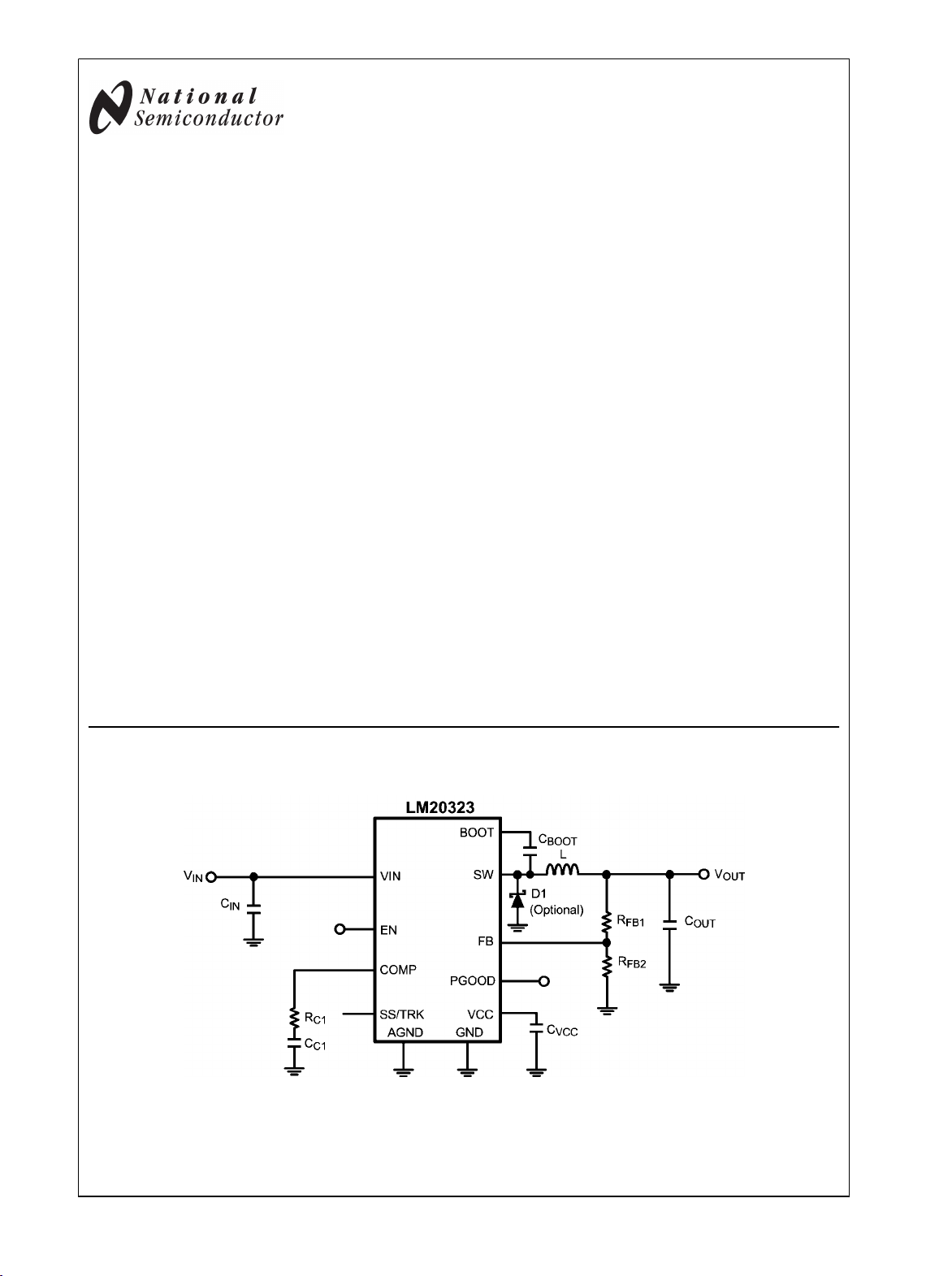
Simplified Application Circuit
30051501
PowerWise® is a registered trademark of National Semiconductor Corporation.
© 2008 National Semiconductor Corporation 300515 www.national.com
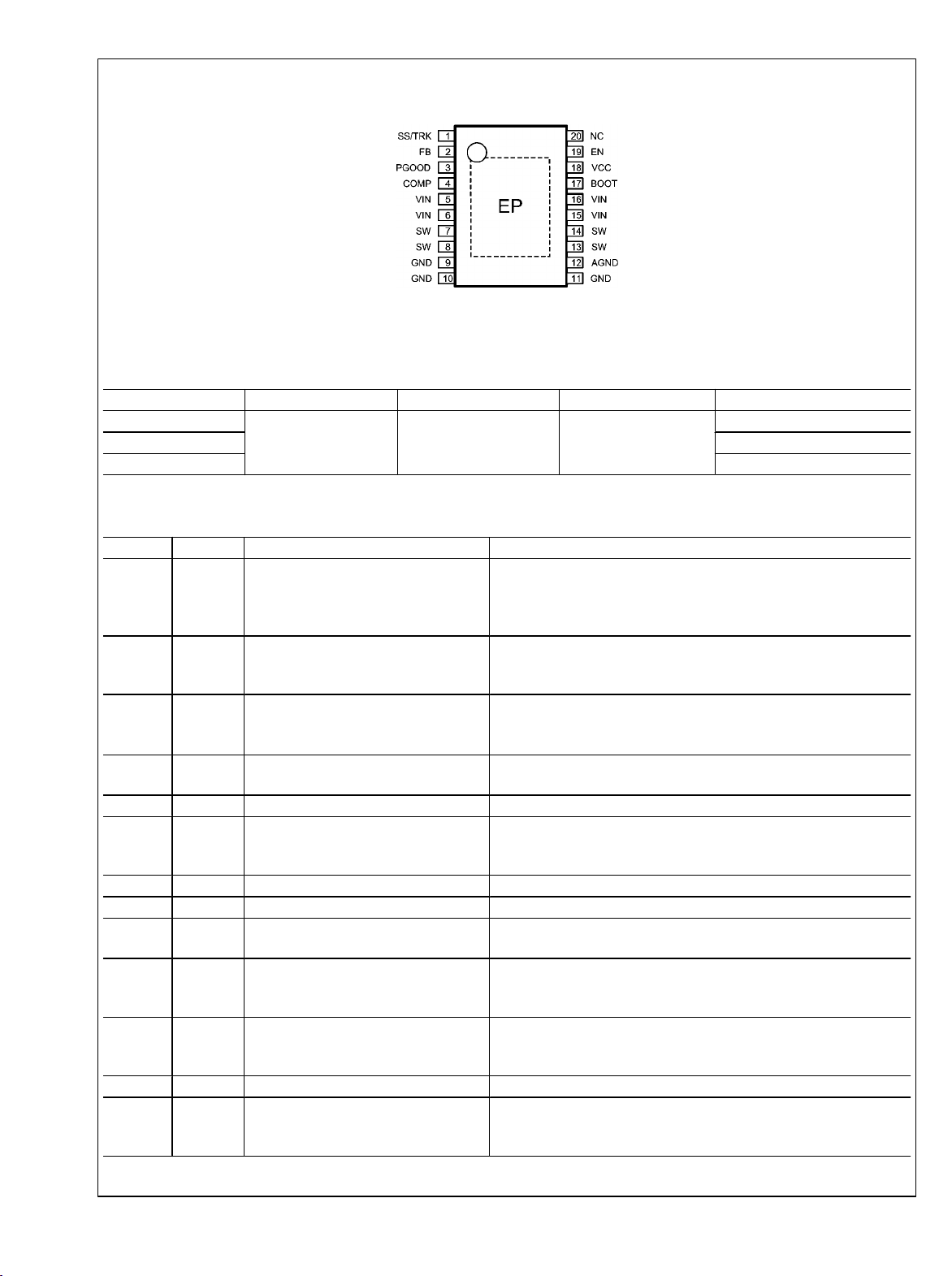
Connection Diagram
LM20323
Top View
eTSSOP-20 Package
30051502
Ordering Information
Order Number Package Type NSC Package Drawing Package Marking Supplied As
LM20323MH eTSSOP-20 MXA20A 20323MH 73 Units per Rail
LM20323MHE 250 Units per Tape and Reel
LM20323MHX 2500 Units per Tape and Reel
Pin Descriptions
Pin(s) Name Description Application Information
1 SS/TRK Soft-Start or Tracking control input An internal 4.5 µA current source charges an external capacitor to set
the soft-start rate. The PWM can track to an external voltage ramp with
a low impedance source. If left open, an internal 1 ms SS ramp is
activated.
2 FB Feedback input to the error amplifier
from the regulated output
3 PGOOD Power good output signal Open drain output indicating the output voltage is regulating within
4 COMP Output of the internal error amplifier and
input to the Pulse Width Modulator
5,6,15,16 VIN Input supply voltage Nominal operating range: 4.5V to 36V.
7,8,13,14 SW Switch pin The drain terminal of the internal Synchronous Rectifier power
9,10,11 GND Ground Internal reference for the power MOSFETs.
12 AGND Analog ground Internal reference for the regulator control functions.
17 BOOT Boost input for bootstrap capacitor An internal diode from VCC to BOOT charges an external capacitor
18 VCC Output of the high voltage linear
regulator. The VCC voltage is regulated
to approximately 5.5V.
19 EN Enable or UVLO input An external voltage divider can be used to set the line undervoltage
20 NC No Connection Recommend connecting this pin to GND.
EP Exposed
Pad
Exposed pad Exposed metal pad on the underside of the package with a weak
This pin is connected to the inverting input of the internal
transconductance error amplifier. An 800 mV reference is internally
connected to the non-inverting input of the error amplifier.
tolerance. A pull-up resistor of 10 kΩ to 100 kΩ is recommended if this
function is used.
The loop compensation network should be connected between the
COMP pin and the AGND pin.
NMOSFET and the source terminal of the internal Control power
NMOSFET.
required from SW to BOOT to power the Control MOSFET gate driver.
VCC tracks VIN up to about 7.2V. Above VIN = 7.2V, VCC is regulated
to approximately 5.5 Volts. A 0.1 µF to 1 µF ceramic decoupling
capacitor is required. The VCC pin is an output only.
lockout threshold. If the EN pin is left unconnected, a 2 µA pull-up
current source pulls the EN pin high to enable the regulator.
electrical connection to GND. Connect this pad to the PC board ground
plane in order to improve heat dissipation.
www.national.com 2
LM20323
Absolute Maximum Ratings (Note 1)
If Military/Aerospace specified devices are required,
please contact the National Semiconductor Sales Office/
Distributors for availability and specifications.
VIN to GND -0.3V to +38V
BOOT to GND -0.3V to +43V
BOOT to SW -0.3V to +7V
SW to GND -0.5V to +38V
VCC to GND -0.3V to +8V
Storage Temperature -65°C to 150°C
ESD Rating
Human Body Model (Note 2) 2kV
Operating Ratings
VIN to GND +4.5V to +36V
Junction Temperature −40°C to + 125°C
SW to GND (Transient) -1.5V (< 20 ns)
FB, EN, SS/TRK, COMP,
-0.3V to +6V
PGOOD to GND
Electrical Characteristics Unless otherwise stated, the following conditions apply: V
= 12V. Limits in standard
VIN
type are for TJ = 25°C only, limits in bold face type apply over the junction temperature (TJ) range of -40°C to +125°C. Minimum
and maximum limits are guaranteed through test, design, or statistical correlation. Typical values represent the most likely
parametric norm at TJ = 25°C, and are provided for reference purposes only.
Symbol Parameter Conditions Min Typ Max Units
V
FB
R
HSW-DS(ON)
R
LSW-DS(ON)
I
Q
I
SD
V
UVLO
V
UVLO(HYS)
V
VCC
I
SS
V
TRKACC
I
BOOT
V
F-BOOT
Feedback Pin Voltage V
= 4.5V to 36V 0.788 0.8 0.812 V
VIN
High-Side MOSFET On-Resistance ISW = 3A 130 225
Low-Side MOSFET On-Resistance ISW = 3A 110 190
Operating Quiescent Current V
= 4.5V to 36V 2.3 3 mA
VIN
Shutdown Quiescent Current VEN = 0V 150 180 µA
VIN Under Voltage Lockout Rising V
VIN
4 4.25 4.5 V
VIN Under Voltage Lockout Hysteresis 350 450 mV
VCC Voltage I
= -5 mA, VEN = 5V 5.5 V
VCC
Soft-Start Pin Source Current VSS = 0V 2 4.5 7 µA
Soft-Start/Track Pin Accuracy VSS = 0.4V -10 5 15 mV
BOOT Diode Leakage V
BOOT Diode Forward Voltage I
= 4V 10 nA
BOOT
= -100 mA 0.9 1.1 V
BOOT
Powergood
V
FB(OVP)
V
FB(OVP-HYS)
V
FB(PG)
V
FB(PG-HYS)
T
PGOOD
I
PGOOD(SNK)
I
PGOOD(SRC)
Over Voltage Protection Rising Threshold V
Over Voltage Protection Hysteresis
PGOOD Threshold, V
Rising V
OUT
PGOOD Hysteresis
Δ
ΔV
FB(OVP)
VFB(OVP)
/ V
FB(PG)
FB(PG)
/ V
/ V
/ V
FB
FB
FB
FB
107 110 112 %
2 3 %
93 95 97 %
2 3 %
PGOOD Delay 20 µs
PGOOD Low Sink Current V
PGOOD High Leakage Current V
= 0.5V 0.6 1 mA
PGOOD
= 5V 5 200 nA
PGOOD
Oscillator
F
SW1
D
MAX
Switching Frequency 470 520 570 kHz
Maximum Duty Cycle I
= 3A 70 %
OUT
Error Amplifier
I
FB
I
COMP(SRC)
I
COMP(SNK)
g
m
A
VOL
Feedback Pin Bias Current VFB = 1V 50 nA
COMP Output Source Current VFB = 0V
V
= 0V
COMP
COMP Output Sink Current VFB = 1.6V
V
= 1.6V
COMP
Error Amplifier DC Transconductance I
= -50 µA to +50 µA 450 515 600 µmho
COMP
200 400 µA
200 350 µA
Error Amplifier Voltage Gain COMP pin open 2000 V/V
GBW Error Amplifier Gain-Bandwidth Product COMP pin open 7 MHz
mΩ
mΩ
3 www.national.com
Symbol Parameter Conditions Min Typ Max Units
Current Limit
LM20323
I
LIM
I
LIMNEG
T
ILIM
Cycle By Cycle Positive Current Limit 4.3 5.2 6.0 A
Cycle By Cycle Negative Current Limit 2.8 A
Cycle By Cycle Current Limit Delay 150 ns
Enable
V
IH_EN
V
EN(HYS)
I
EN
EN Pin Rising Threshold 1.2 1.25 1.3 V
EN Pin Hysteresis 50 mV
EN Source Current VEN = 0V, V
= 12V 2 µA
VIN
Thermal Shutdown
T
T
SD(HYS)
SD
Thermal Shutdown 170 °C
Thermal Shutdown Hysteresis 20 °C
Thermal Resistance
θ
JC
θ
JA
Note 1: Absolute Maximum Ratings indicate limits beyond witch damage to the device may occur. Operating Ratings indicate conditions for which the device is
intended to be functional, but do not guarantee specific performance limits. For guaranteed specifications and test conditions, see the Electrical Characteristics.
Note 2: The human body model is a 100 pF capacitor discharged through a 1.5 kΩ resistor to each pin.
Note 3: Measured on a 4 layer 2" x 2" PCB with 1 oz. copper weight inner layers and 2 oz. outer layers.
Junction to Case 5.6 °C/W
Junction to Ambient (Note 3) 0 LFM airflow 27 °C/W
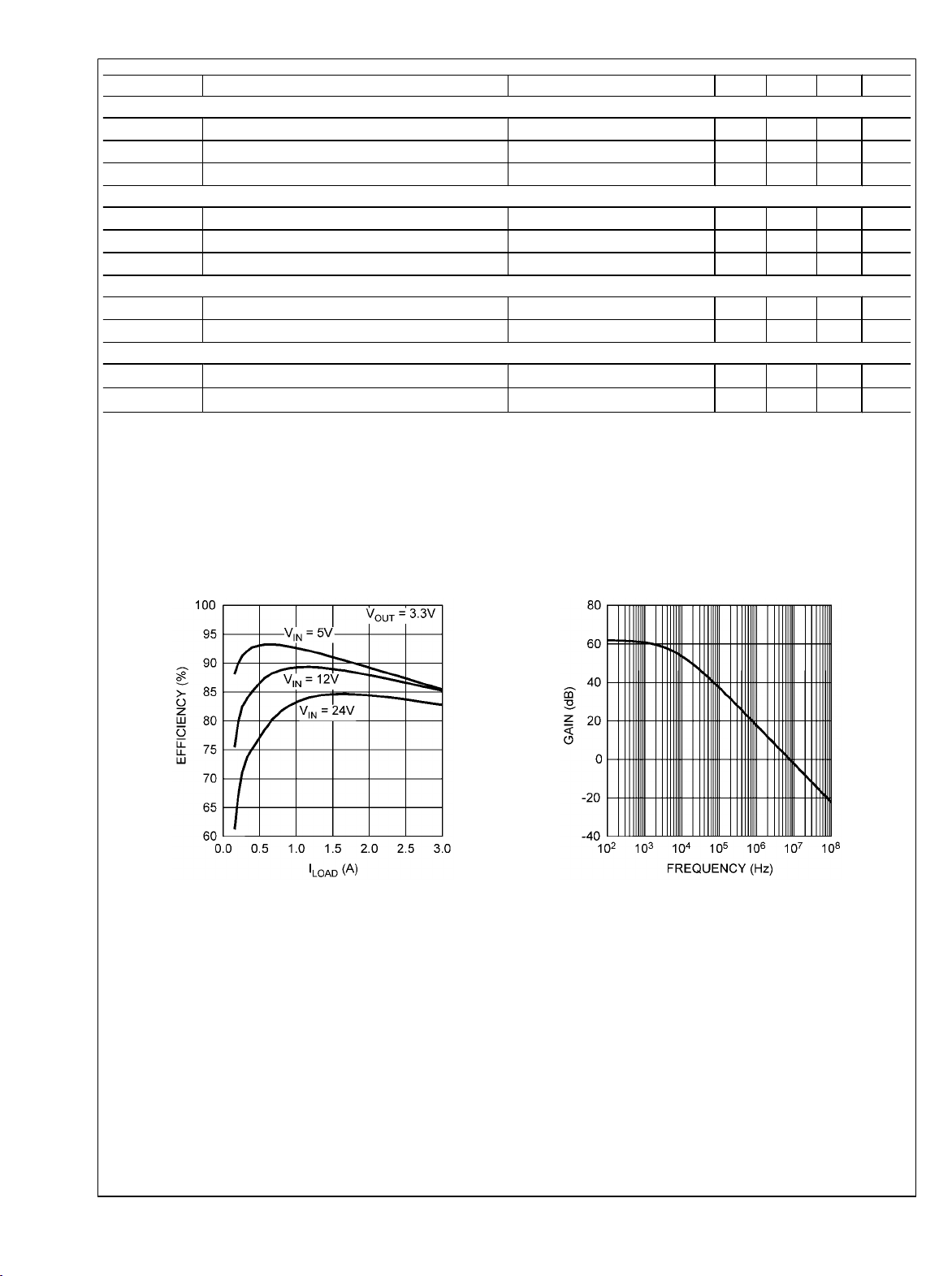
Typical Performance Characteristics Unless otherwise specified: V
= 12V, V
VIN
CSS = 100nF, TA = 25°C for efficiency curves, loop gain plots and waveforms, and TJ = 25°C for all others.
Efficiency vs. Load Current
30051504
Error Amplifier Gain
= 3.3V, L= 5.6 µH,
OUT
30051505
www.national.com 4
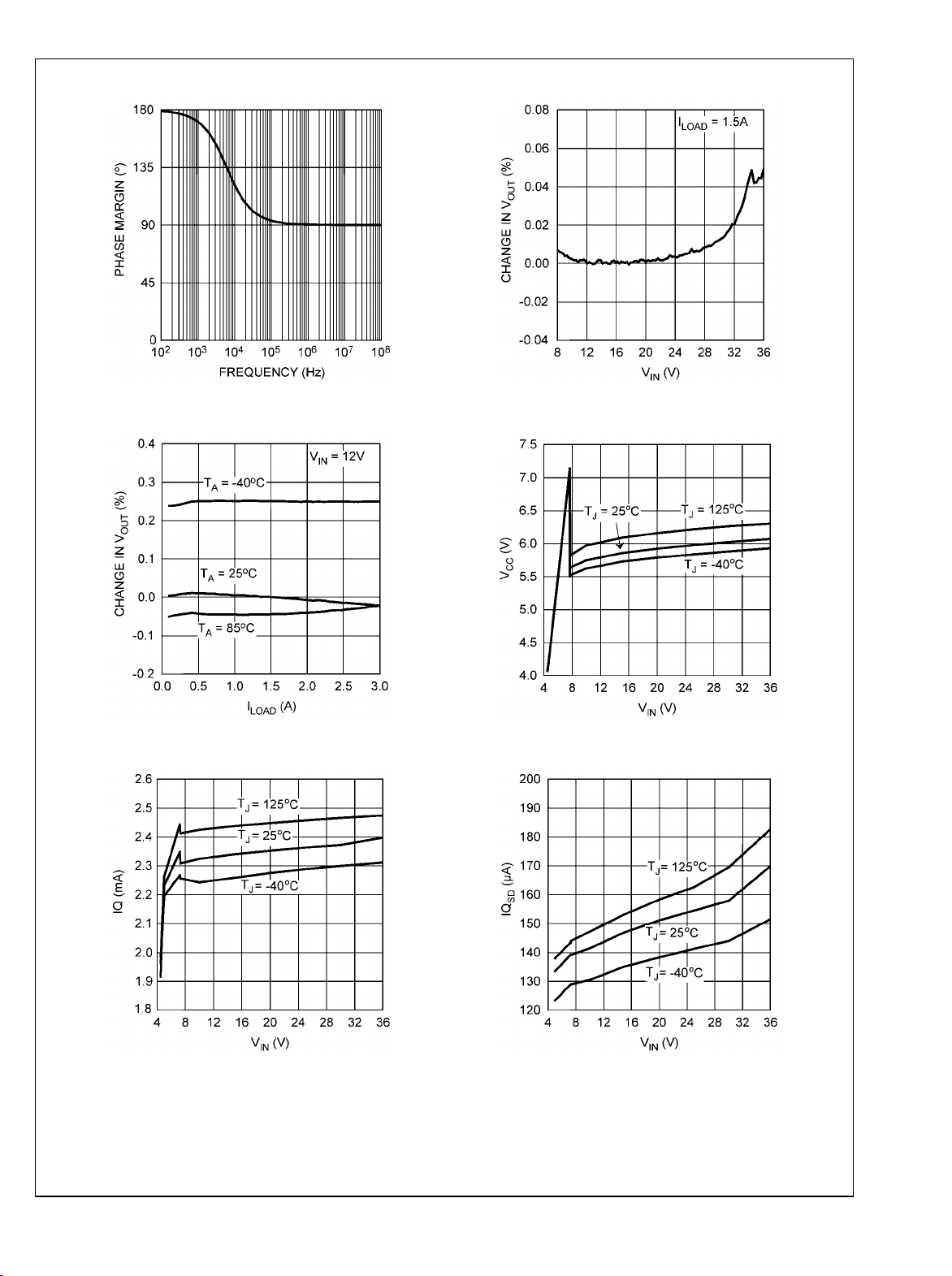
LM20323
Error Amplifier Phase
Load Regulation
30051506
Line Regulation
VCC vs. V
IN
30051507
Non-Switching IQ vs. V
30051586
IN
30051509
Shutdown IQ vs. V
IN
30051508
30051510
5 www.national.com
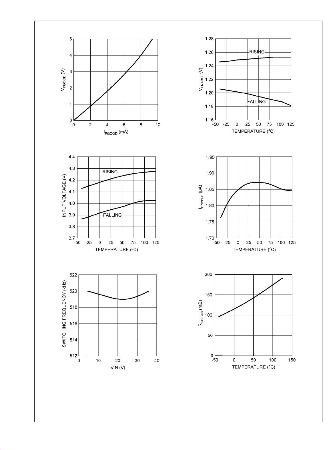
LM20323
PGOOD Output Low Level Voltage vs. I
PGOOD
Enable Threshold and Hysteresis vs. Temperature
30051519
UVLO Threshold and Hysteresis vs. Temperature
30051595
Oscillator Frequency vs. V
IN
30051521
Enable Current vs. Temperature
30051522
High-Side FET Resistance vs. Temperature
30051554
www.national.com 6
30051555

LM20323
Load Transient Response
Peak Current Limit vs. Temperature
Low-Side FET Resistance vs. Temperature
30051556
30051557
Startup with Prebiased Output
Startup with CSS = 0
30051558
30051559
30051579
Startup with CSS = 100 nF
30051560
7 www.national.com

LM20323
Startup with Applied Track Signal
30051581
www.national.com 8

Block Diagram
LM20323
30051523
9 www.national.com

Operation Description
GENERAL
LM20323
The LM20323 switching regulator features all of the functions
necessary to implement an efficient buck regulator using a
minimum number of external components. This easy to use
regulator features two integrated switches and is capable of
supplying up to 3A of continuous output current. The regulator
utilizes peak current mode control with nonlinear slope compensation to optimize stability and transient response over the
entire output voltage range. Peak current mode control also
provides inherent line feed-forward, cycle-by-cycle current
limiting and easy loop compensation. The 500kHz switching
frequency minimizes the inductor size while keeping switching losses low allowing use of a small inductor while still
achieving efficiencies as high as 93%. The precision internal
voltage reference allows the output to be set as low as 0.8V.
Fault protection features include: current limiting, thermal
shutdown, over voltage protection, and shutdown capability.
The device is available in the eTSSOP-20 package featuring
an exposed pad to aid thermal dissipation. The typical application circuit for the LM20323 is shown in Figure 1 in the
design guide.
PRECISION ENABLE
The enable (EN) pin allows the output of the device to be enabled or disabled with an external control signal. This pin is a
precision analog input that enables the device when the voltage exceeds 1.25V (typical). The EN pin has 50 mV of hysteresis and will disable the output when the enable voltage
falls below 1.2V (typical). If the EN pin is not used, it should
be disconnected so the internal 2 µA pull-up will default this
function to the enabled condition. Since the enable pin has a
precise turn-on threshold it can be used along with an external
resistor divider network from VIN to configure the device to
turn-on at a precise input voltage. The precision enable circuitry will remain active even when the device is disabled.
PEAK CURRENT MODE CONTROL
In most cases, the peak current mode control architecture
used in the LM20323 only requires two external components
to achieve a stable design. The compensation can be selected to accommodate any capacitor type or value. The external
compensation also allows the user to set the crossover frequency and optimize the transient performance of the device.
For duty cycles above 50% all peak current mode control buck
converters require the addition of an artificial ramp to avoid
sub-harmonic oscillation. This artificial linear ramp is commonly referred to as slope compensation. What makes the
LM20323 unique is the amount of slope compensation will
change depending on the output voltage. When operating at
high output voltages the device will have more slope compensation than when operating at lower output voltages. This
is accomplished in the LM20323 by using a non-linear
parabolic ramp for the slope compensation. The parabolic
slope compensation of the LM20323 is an improvement over
the traditional linear slope compensation because it optimizes
the stability of the device over the entire output voltage range.
CURRENT LIMIT
The precise current limit enables the device to operate with
smaller inductors that have lower saturation currents. When
the peak inductor current reaches the current limit threshold,
an over current event is triggered and the internal high-side
FET turns off and the low-side FET turns on, allowing the inductor current to ramp down until the next switching cycle. For
each sequential over-current event, the reference voltage is
decremented and PWM pulses are skipped resulting in a current limit that does not aggressively fold back for brief overcurrent events, while at the same time providing frequency
and voltage foldback protection during hard short circuit conditions.
SOFT-START AND VOLTAGE TRACKING
The SS/TRK pin is a dual function pin that can be used to set
the startup time or track an external voltage source. The startup or soft-start time can be adjusted by connecting a capacitor
from the SS/TRK pin to ground. The soft-start feature allows
the regulator output to gradually reach the steady state operating point, thus reducing stresses on the input supply and
controlling startup current. If no soft-start capacitor is used the
device defaults to the internal soft-start circuitry resulting in a
startup time of approximately 1 ms. For applications that require a monotonic startup or utilize the PGOOD pin, an external soft-start capacitor is recommended. The SS/TRK pin
can also be set to track an external voltage source. The tracking behavior can be adjusted by two external resistors connected to the SS/TRK pin as shown in Figure 6 in the design
guide.
PRE-BIAS STARTUP CAPABILITY
The LM20323 is in a pre-biased state when it starts up with
an output voltage greater than zero. This often occurs in many
multi-rail applications such as when powering an FPGA,
ASIC, or DSP. In these applications the output can be prebiased through parasitic conduction paths from one supply
rail to another. Even though the LM20323 is a synchronous
converter, it will not pull the output low when a pre-bias condition exists. During start up the LM20323 will not sink current
until the soft-start voltage exceeds the voltage on the FB pin.
Since the device cannot sink current, it protects the load from
damage that might otherwise occur if current is conducted
through the parasitic paths of the load.
POWER GOOD AND OVER VOLTAGE FAULT HANDLING
The LM20323 has built in under and over voltage comparators that control the power switches. Whenever there is an
excursion in output voltage above the set OVP threshold, the
part will terminate the present on-pulse, turn-on the low-side
FET, and pull the PGOOD pin low. The low-side FET will remain on until either the FB voltage falls back into regulation
or the negative current limit is triggered which in turn tri-states
the FETs. If the output reaches the UVP threshold the part will
continue switching and the PGOOD pin will be deasserted
and go low. Typical values for the PGOOD resistor are on the
order of 100 kΩ or less. To avoid false tripping during transient
glitches the PGOOD pin has 20 µs of built in deglitch time to
both rising and falling edges.
UVLO
The LM20323 has an internal under-voltage lockout protection circuit that keeps the device from switching until the input
voltage reaches 4.25V (typical). The UVLO threshold has 350
mV of hysteresis that keeps the device from responding to
power-on glitches during start up. If desired the turn-on point
of the supply can be changed by using the precision enable
pin and a resistor divider network connected to VIN as shown
in Figure 5 in the design guide.
THERMAL PROTECTION
Internal thermal shutdown circuitry is provided to protect the
integrated circuit in the event that the maximum junction temperature is exceeded. When activated, typically at 170°C, the
LM20323 tri-states the power FETs and resets soft-start. After
www.national.com 10

the junction cools to approximately 150°C, the part starts up
using the normal start up routine. This feature is provided to
prevent catastrophic failures from accidental device overheating.
Design Guide
This section walks the designer through the steps necessary
to select the external components to build a fully functional
power supply. As with any DC-DC converter numerous tradeoffs are possible to optimize the design for efficiency, size, or
performance. These will be taken into account and highlighted throughout this discussion. To facilitate component selection discussions the circuit shown in Figure 1 below may be
used as a reference. Unless otherwise indicated, all formulas
assume units of amps (A) for current, farads (F) for capacitance, henries (H) for inductance and volts (V) for voltages.
30051567
FIGURE 2. Switch and Inductor Current Waveforms
If needed, slightly smaller value inductors can be used, however, the peak inductor current, I
below the peak current limit of the device. In general, the in-
+ ΔiL/2, should be kept
OUT
ductor ripple current, ΔiL, should be more than 10% of the
rated output current to provide adequate current sense information for the current mode control loop. If the ripple current
in the inductor is too low, the control loop will not have sufficient current sense information and can be prone to instability.
LM20323
30051529
FIGURE 1. Typical Application Circuit
The first equation to calculate for any buck converter is dutycycle. Ignoring conduction losses associated with the FETs
and parasitic resistances it can be approximated by:
INDUCTOR SELECTION (L)
The inductor value is determined based on the operating frequency, load current, ripple current and duty cycle.
The inductor selected should have a saturation current rating
greater than the peak current limit of the device. Keep in mind
the specified current limit does not account for delay of the
current limit comparator, therefore the current limit in the application may be higher than the specified value. To optimize
the performance and prevent the device from entering current
limit at maximum load, the inductance is typically selected
such that the ripple current, ΔiL, is not greater than 30% of the
rated output current. Figure 2 illustrates the switch and inductor ripple current waveforms. Once the input voltage, output voltage, operating frequency and desired ripple current
are known, the minimum value for the inductor can be calculated by the formula shown below:
OUTPUT CAPACITOR SELECTION (C
The output capacitor, C
and provides a source of charge for transient load conditions.
, filters the inductor ripple current
OUT
OUT
)
A wide range of output capacitors may be used with the
LM20323 that provide excellent performance. The best performance is typically obtained using ceramic, SP or OSCON
type chemistries. Typical trade-offs are that the ceramic capacitor provides extremely low ESR to reduce the output
ripple voltage and noise spikes, while the SP and OSCON
capacitors provide a large bulk capacitance in a small volume
for transient loading conditions.
When selecting the value for the output capacitor, the two
performance characteristics to consider are the output voltage ripple and transient response. The output voltage ripple
can be approximated by using the following formula:
where, ΔV
at the power supply output, R
of the output capacitor, fSW(Hz) is the switching frequency,
and C
The amount of output ripple that can be tolerated is applica-
(V) is the amount of peak to peak voltage ripple
OUT
(F) is the output capacitance used in the design.
OUT
(Ω) is the series resistance
ESR
tion specific; however a general recommendation is to keep
the output ripple less than 1% of the rated output voltage.
Keep in mind ceramic capacitors are sometimes preferred
because they have very low ESR; however, depending on
package and voltage rating of the capacitor the value of the
capacitance can drop significantly with applied voltage. The
output capacitor selection will also affect the output voltage
droop during a load transient. The peak droop on the output
voltage during a load transient is dependent on many factors;
however, an approximation of the transient droop ignoring
loop bandwidth can be obtained using the following equation:
11 www.national.com

where, C
L (H) is the value of the inductor, V
voltage drop ignoring loop bandwidth considerations, ΔI
LM20323
STEP
capacitor ESR, VIN (V) is the input voltage, and V
(F) is the minimum required output capacitance,
OUT
DROOP
(A) is the load step change, R
(Ω) is the output
ESR
(V) is the output
the set regulator output voltage. Both the tolerance and voltage coefficient of the capacitor should be examined when
designing for a specific output ripple or transient droop target.
INPUT CAPACITOR SELECTION
Good quality input capacitors are necessary to limit the ripple
voltage at the VIN pin while supplying most of the switch current during the on-time. In general it is recommended to use
a ceramic capacitor for the input as they provide both a low
impedance and small footprint. One important note is to use
a good dielectric for the ceramic capacitor such as X5R or
X7R. These provide better over temperature performance
and also minimize the DC voltage derating that occurs on Y5V
capacitors. The input capacitors C
placed as close as possible to the VIN and GND pins on both
and C
IN1
IN2
sides of the device.
Non-ceramic input capacitors should be selected for RMS
current rating and minimum ripple voltage. A good approximation for the required ripple current rating is given by the
relationship:
As indicated by the RMS ripple current equation, highest requirement for RMS current rating occurs at 50% duty cycle.
For this case, the RMS ripple current rating of the input capacitor should be greater than half the output current. For best
performance, low ESR ceramic capacitors should be placed
in parallel with higher capacitance capacitors to provide the
best input filtering for the device.
OUT-
(V) is
OUT
should be
capacitor, inductor, load and the device itself. Table 2 below
gives values for the compensation network that will result in
a stable system when using a 150 µF, 6.3V POSCAP (6TPB150MAZB) output capacitor.
TABLE 2. Recommended Compensation for
C
= 150 µF, I
OUT
V
V
IN
OUT
L (µH)
= 3A
OUT
RC (kΩ)
CC1 (nF)
12 5 6.8 45.3 4.7
12 3.3 5.6 32.4 4.7
12 2.5 4.7 30.9 3.3
12 1.5 3.3 19.1 3.3
12 1.2 2.2 21.5 2.2
12 0.8 1.5 15 2.2
5 3.3 2.2 29.4 2.2
5 2.5 3.3 37.4 2.2
5 1.5 2.2 26.7 2.2
5 1.2 2 22.1 2.2
5 0.8 1.5 15 2.2
If the desired solution differs from the table above the loop
transfer function should be analyzed to optimize the loop
compensation. The overall loop transfer function is the product of the power stage and the feedback network transfer
functions. For stability purposes, the objective is to have a
loop gain slope that is -20dB/decade from a very low frequency to beyond the crossover frequency. Figure 3 shows the
transfer functions for power stage, feedback/compensation
network, and the resulting compensated loop for the
LM20323.
SETTING THE OUTPUT VOLTAGE (R
The resistors R
voltage for the device. provides suggestions for R
R
for common output voltages.
FB2
FB1
and R
are selected to set the output
FB2
TABLE 1. Suggested Values for R
R
(kΩ) R
FB1
FB2
(kΩ)
FB1
V
FB1
OUT
, R
FB2
and R
)
and
FB1
FB2
short open 0.8
4.99 10 1.2
8.87 10.2 1.5
12.7 10.2 1.8
21.5 10.2 2.5
31.6 10.2 3.3
52.3 10 5.0
If different output voltages are required, R
lected to be between 4.99 kΩ to 49.9 kΩ and R
calculated using the equation below.
should be se-
FB2
FB1
can be
LOOP COMPENSATION (RC1, CC1)
The purpose of loop compensation is to meet static and dynamic performance requirements while maintaining adequate
stability. Optimal loop compensation depends on the output
30051572
FIGURE 3. LM20323 Loop Compensation
www.national.com 12

LM20323
The power stage transfer function is dictated by the modulator, output LC filter, and load; while the feedback transfer
function is set by the feedback resistor ratio, error amp gain
and external compensation network.
To achieve a -20dB/decade slope, the error amplifier zero,
located at f
ter pole (f
, should be positioned to cancel the output fil-
Z(EA)
).
P(FIL)
Compensation of the LM20323 is achieved by adding an RC
network as shown in Figure 4 below.
30051545
FIGURE 4. Compensation Network for LM20323
A good starting value for CC1 for most applications is 2.2 nF.
Once the value of CC1 is chosen the value of RC1 should be
approximated using the equation below to cancel the output
filter pole (f
) as shown in Figure 3.
P(FIL)
A higher crossover frequency can be obtained, usually at the
expense of phase margin, by lowering the value of CC1 and
recalculating the value of RC1. Likewise, increasing CC1 and
recalculating RC1 will provide additional phase margin at a
lower crossover frequency. As with any attempt to compensate the LM20323 the stability of the system should be verified
for desired transient droop and settling time.
For low duty cycle operation, when the on-time of the switch
node is less than 200ns, an additional capacitor (CC2) should
be added from the COMP pin to AGND. The recommended
value of this capacitor is 20pF. If low duty cycle jitter on the
switch node is observed, the value of this capacitor can be
increased to improve noise immunity; however, values much
larger than 100pF will cause the pole f
frequency degrading the loop stability.
BOOT CAPACITOR (C
BOOT
)
to move to a lower
P2(EA)
The LM20323 integrates an N-channel buck switch and associated floating high voltage level shift / gate driver. This gate
driver circuit works in conjunction with an internal diode and
an external bootstrap capacitor. A 0.1 µF ceramic capacitor,
connected with short traces between the BOOT pin and SW
pin, is recommended. During the off-time of the buck switch,
the SW pin voltage is approximately 0V and the bootstrap capacitor is charged from VCC through the internal bootstrap
diode.
mended for most applications. The VCC regulator should not
be used for other functions since it isn't protected against
short circuit.
SETTING THE START UP TIME (CSS)
The addition of a capacitor connected from the SS pin to
ground sets the time at which the output voltage will reach the
final regulated value. Larger values for CSS will result in longer
start up times. Table 3, shown below provides a list of soft
start capacitors and the corresponding typical start up times.
TABLE 3. Start Up Times for Different Soft-Start
Capacitors
Start Up Time (ms) CSS (nF)
1 none
5 33
10 68
15 100
20 120
If different start up times are needed the equation shown below can be used to calculate the start up time.
As shown above, the start up time is influenced by the value
of the soft-start capacitor CSS and the 4.5 µA soft-start pin
current ISS.
While the soft-start capacitor can be sized to meet many start
up requirements, there are limitations to its size. The soft-start
time can never be faster than 1 ms due to the internal default
1 ms start up time. When the device is enabled there is an
approximate time interval of 50 µs when the soft-start capacitor will be discharged just prior to the soft-start ramp. If the
enable pin is rapidly pulsed or the soft-start capacitor is large
there may not be enough time for CSS to completely discharge
resulting in start up times less than predicted. To aid in discharging of soft-start capacitor during long disable periods an
external 1MΩ resistor from SS/TRK to ground can be used
without greatly affecting the start up time.
USING PRECISION ENABLE AND POWER GOOD
The precision enable (EN) and power good (PGOOD) pins of
the LM20323 can be used to address many sequencing requirements. The turn-on of the LM20323 can be controlled
with the precision enable pin by using two external resistors
as shown in Figure 5 .
SUB-REGULATOR BYPASS CAPACITOR (C
VCC
)
The capacitor at the VCC pin provides noise filtering for the
internal sub-regulator. The recommended value of C
should be no smaller than 0.1 µF and no greater than 1 µF.
VCC
The capacitor should be a good quality ceramic X5R or X7R
capacitor. In general, a 1 µF ceramic capacitor is recom-
30051562
FIGURE 5. Sequencing LM20323 with Precision Enable
13 www.national.com

The value for resistor RB can be selected by the user to control
the current through the divider. Typically this resistor will be
selected to be between 1 kΩ and 49.9 kΩ. Once the value for
LM20323
RB is chosen the resistor RA can be solved using the equation
below to set the desired turn-on voltage.
When designing for a specific turn-on threshold (VTO) the tolerance on the input supply, enable threshold (V
external resistors need to be considered to ensure proper
turn-on of the device.
The LM20323 features an open drain power good (PGOOD)
pin to sequence external supplies or loads and to provide fault
detection. This pin requires an external resistor (RPG) to pull
PGOOD high when the output is within the PGOOD tolerance
window. Typical values for this resistor range from 10 kΩ to
100 kΩ.
TRACKING AN EXTERNAL SUPPLY
By using a properly chosen resistor divider network connected to the SS/TRK pin, as shown in Figure 6, the output of the
LM20323 can be configured to track an external voltage
source to obtain a simultaneous or ratiometric start up.
IH_EN
), and
30051578
30051561
FIGURE 6. Tracking an External Supply
Since the soft-start charging current ISS is always present on
the SS/TRK pin, the size of R2 should be less than 10 kΩ to
minimize the errors in the tracking output. Once a value for
R2 is selected the value for R1 can be calculated using appropriate equation in Figure 7, to give the desired start up.
Figure 6 shows two common start up sequences; the top
waveform shows a simultaneous start up while the waveform
at the bottom illustrates a ratiometric start up.
FIGURE 7. Common Start Up Sequences
A simultaneous start up is preferred when powering most FPGAs, DSPs, or other microprocessors. In these systems the
higher voltage, V
voltage, V
vides a more robust power up for these applications since it
OUT2
, usually powers the I/O, and the lower
OUT1
, powers the core. A simultaneous start up pro-
avoids turning on any parasitic conduction paths that may exist between the core and the I/O pins of the processor.
The second most common power on behavior is known as a
ratiometric start up. This start up is preferred in applications
where both supplies need to be at the final value at the same
time.
Similar to the soft-start function, the fastest start up possible
is 1ms regardless of the rise time of the tracking voltage.
When using the track feature the final voltage seen by the SS/
TRACK pin should exceed 1V to provide sufficient overdrive
and transient immunity.
BENEFIT OF AN EXTERNAL SCHOTTKY
The LM20323 employs a 40ns dead time between conduction
of the control and synchronous FETs in order to avoid the
situation where both FETs simultaneously conduct, causing
shoot-through current. During the dead time, the body diode
of the synchronous FET acts as a free-wheeling diode and
conducts the inductor current. The structure of the high voltage DMOS is optimized for high breakdown voltage, but this
typically leads to inefficient body diode conduction due to the
reverse recovery charge. The loss associated with the reverse recovery of the body diode of the synchronous FET
manifests itself as a loss proportional to load current and
switching frequency. The additional efficiency loss becomes
apparent at higher input voltages and switching frequencies.
One simple solution is to use a small 1A external Schottky
diode between SW and GND as shown in Figure 12. The external Schottky diode effectively conducts all inductor current
during the dead time, minimizing the current passing through
www.national.com 14

the synchronous MOSFET body diode and eliminating reverse recovery losses.
The external Schottky conducts currents for a very small portion of the switching cycle, therefore the average current is
low. An external Schottky rated for 1A will improve efficiency
by several percent in some applications. A Schottky rated at
a higher current will not significantly improve efficiency and
may be worse due to the increased reverse capacitance. The
forward voltage of the synchronous MOSFET body diode is
approximately 700 mV, therefore an external Schottky with a
forward voltage less than or equal to 700 mV should be selected to ensure the majority of the dead time current is carried
by the Schottky.
THERMAL CONSIDERATIONS
The thermal characteristics of the LM20323 are specified using the parameter θJA, which relates the junction temperature
to the ambient temperature. Although the value of θJA is dependant on many variables, it still can be used to approximate
the operating junction temperature of the device.
To obtain an estimate of the device junction temperature, one
may use the following relationship:
TJ = PD x θJA + T
A
and
PD = PIN x (1 - Efficiency) - 1.1 x (I
OUT
)2 x DCR
Where:
TJ is the junction temperature in °C.
PIN is the input power in Watts (PIN = VIN x IIN).
θJA is the junction to ambient thermal resistance for the
LM20323.
TA is the ambient temperature in °C.
I
is the output load current.
OUT
DCR is the inductor series resistance.
It is important to always keep the operating junction temper-
ature (TJ) below 125°C for reliable operation. If the junction
temperature exceeds 170°C the device will cycle in and out
of thermal shutdown. If thermal shutdown occurs it is a sign
of inadequate heatsinking or excessive power dissipation in
the device.
Figure 8 and Figure 9 can be used as a guide to avoid exceeding the maximum junction temperature of 125°C provided an external 1A Schottky diode, such as Central
Semiconductor's CMMSH1-40-NST, is used to improve reverse recovery losses.
30051588
FIGURE 8. Safe Thermal Operating Areas (I
FIGURE 9. Safe Thermal Operating Areas (I
OUT
30051590
OUT
= 3A)
= 2.5A)
The dashed lines in the figures above show an approximation
of the minimum and maximum duty cycle limitations; while,
the solid lines define areas of operation for a given ambient
temperature. This data for the figure was derived assuming
the device is operating at 3A continuous output current on a
4 layer PCB with an copper area greater than 4 square inches
exhibiting a thermal characteristic less than 27 °C/W. Since
the internal losses are dominated by the FETs a slight reduction in current by 500mA allows for much larger regions of
operation, as shown in Figure 9.
Figure 10, shown below, provides a better approximation of
the θJA for a given PCB copper area. The PCB used in this
test consisted of 4 layers: 1oz. copper was used for the internal layers while the external layers were plated to 2oz. copper
weight. To provide an optimal thermal connection, a 5 x 4 array of 12 mil thermal vias located under the thermal pad was
used to connect the 4 layers.
LM20323
15 www.national.com

LM20323
FIGURE 10. Thermal Resistance vs PCB Area (4 Layer
Board)
PCB LAYOUT CONSIDERATIONS
PC board layout is an important part of DC-DC converter design. Poor board layout can disrupt the performance of a DCDC converter and surrounding circuitry by contributing to EMI,
ground bounce, and resistive voltage loss in the traces. These
can send erroneous signals to the DC-DC converter resulting
in poor regulation or instability.
Good layout can be implemented by following a few simple
design rules.
1. Minimize area of switched current loops. In a buck regulator
there are two loops where currents are switched at high slew
rates. The first loop starts from the input capacitor, to the regulator VIN pin, to the regulator SW pin, to the inductor then
out to the output capacitor and load. The second loop starts
from the output capacitor ground, to the regulator GND pins,
to the inductor and then out to the load (see Figure 11). To
minimize both loop areas the input capacitor should be placed
as close as possible to the VIN pin. Grounding for both the
30051587
input and output capacitor should consist of a small localized
top side plane that connects to GND and the exposed pad
(EP). The inductor should be placed as close as possible to
the SW pin and output capacitor.
2. Minimize the copper area of the switch node. Since the
LM20323 has the SW pins on opposite sides of the package
it is recommended that the SW pins should be connected with
a trace that runs around the package. The inductor should be
placed at an equal distance from the SW pins using 100 mil
wide traces to minimize capacitive and conductive losses.
3. Have a single point ground for all device grounds located
under the EP. The ground connections for the compensation,
feedback, and soft-start components should be connected
together then routed to the EP pin of the device. The AGND
pin should connect to GND under the EP. If not properly handled poor grounding can result in degraded load regulation or
erratic switching behavior.
4. Minimize trace length to the FB pin. Since the feedback
node can be high impedance the trace from the output resistor
divider to FB pin should be as short as possible. This is most
important when high value resistors are used to set the output
voltage. The feedback trace should be routed away from the
SW pin and inductor to avoid contaminating the feedback signal with switch noise.
5. Make input and output bus connections as wide as possible. This reduces any voltage drops on the input or output of
the converter and can improve efficiency. Voltage accuracy
at the load is important so make sure feedback voltage sense
is made at the load. Doing so will correct for voltage drops at
the load and provide the best output accuracy.
6. Provide adequate device heatsinking. For most 3A designs
a four layer board is recommended. Use as many vias as is
possible to connect the EP to the power plane heatsink. For
best results use a 5x4 via array with a minimum via diameter
of 12 mils. "Via tenting" with the solder mask may be necessary to prevent wicking of the solder paste applied to the EP.
See the Thermal Considerations section to ensure enough
copper heatsinking area is used to keep the junction temperature below 125°C.
FIGURE 11. Schematic of LM20323 Highlighting Layout Sensitive Nodes
www.national.com 16
30051546

LM20323
FIGURE 12. Typical Application Schematic
Bill of Materials (VIN = 12V, V
ID Qty Part Number Size Description Vendor
U1 1 LM20323MH eTSSOP-20 IC, Switching Regulator NSC
C1 1 C3225X5R1E226M 1210 22µF, X5R, 25V, 20% TDK
C2, C3 2 GRM21BR61E475KA12L 0805 4.7µF, X5R, 25V, 10% MuRata
C5, C6 1 C1608X7R1H104K 0603 100nF, X7R, 50V, 10% TDK
C4 1 C1608X5R1A105K 0603 1µF, X7R, 10V, 10% TDK
C7 1 C1608C0G1H100J 0603 10pF, C0G, 50V, 5% TDK
C8 1 C1608C0G1H102J 0603 1nF, C0G, 50V, 5% TDK
C9 1 6TPB150MAZB B 150µF,POSCAP, 6.3V, 20% Sanyo
D1 1 CMMSH1-40-NST SOD123 Vr = 40V, Io = 1A, Vf = 0.55V Central
L1 1 IHLP4040DZER5R6M01 IHLP4040 5.6µH, 0.018 Ohms, 16A Vishay
R1, R4 2 CRCW06031002F 0603
R2 1 CRCW06034992F 0603
R3 1 CRCW06033092F 0603
= 3.3V, I
OUT
OUT
= 3A)
10kΩ, 1%
49.9kΩ, 1%
30.9kΩ, 1%
Semiconductor
Vishay
Vishay
Vishay
30051544
17 www.national.com

Physical Dimensions inches (millimeters) unless otherwise noted
LM20323
20-Lead eTSSOP Package
NS Package Number MXA20A
www.national.com 18

Notes
LM20323
19 www.national.com

Notes
For more National Semiconductor product information and proven design tools, visit the following Web sites at:
Products Design Support
Amplifiers www.national.com/amplifiers WEBENCH www.national.com/webench
Audio www.national.com/audio Analog University www.national.com/AU
Clock Conditioners www.national.com/timing App Notes www.national.com/appnotes
Data Converters www.national.com/adc Distributors www.national.com/contacts
Displays www.national.com/displays Green Compliance www.national.com/quality/green
Ethernet www.national.com/ethernet Packaging www.national.com/packaging
Interface www.national.com/interface Quality and Reliability www.national.com/quality
LVDS www.national.com/lvds Reference Designs www.national.com/refdesigns
Power Management www.national.com/power Feedback www.national.com/feedback
Switching Regulators www.national.com/switchers
LDOs www.national.com/ldo
LED Lighting www.national.com/led
500 kHz Synchronous Buck Regulator
PowerWise www.national.com/powerwise
®
Serial Digital Interface (SDI) www.national.com/sdi
Temperature Sensors www.national.com/tempsensors
Wireless (PLL/VCO) www.national.com/wireless
THE CONTENTS OF THIS DOCUMENT ARE PROVIDED IN CONNECTION WITH NATIONAL SEMICONDUCTOR CORPORATION
(“NATIONAL”) PRODUCTS. NATIONAL MAKES NO REPRESENTATIONS OR WARRANTIES WITH RESPECT TO THE ACCURACY
OR COMPLETENESS OF THE CONTENTS OF THIS PUBLICATION AND RESERVES THE RIGHT TO MAKE CHANGES TO
SPECIFICATIONS AND PRODUCT DESCRIPTIONS AT ANY TIME WITHOUT NOTICE. NO LICENSE, WHETHER EXPRESS,
IMPLIED, ARISING BY ESTOPPEL OR OTHERWISE, TO ANY INTELLECTUAL PROPERTY RIGHTS IS GRANTED BY THIS
DOCUMENT.
TESTING AND OTHER QUALITY CONTROLS ARE USED TO THE EXTENT NATIONAL DEEMS NECESSARY TO SUPPORT
NATIONAL’S PRODUCT WARRANTY. EXCEPT WHERE MANDATED BY GOVERNMENT REQUIREMENTS, TESTING OF ALL
PARAMETERS OF EACH PRODUCT IS NOT NECESSARILY PERFORMED. NATIONAL ASSUMES NO LIABILITY FOR
APPLICATIONS ASSISTANCE OR BUYER PRODUCT DESIGN. BUYERS ARE RESPONSIBLE FOR THEIR PRODUCTS AND
APPLICATIONS USING NATIONAL COMPONENTS. PRIOR TO USING OR DISTRIBUTING ANY PRODUCTS THAT INCLUDE
NATIONAL COMPONENTS, BUYERS SHOULD PROVIDE ADEQUATE DESIGN, TESTING AND OPERATING SAFEGUARDS.
EXCEPT AS PROVIDED IN NATIONAL’S TERMS AND CONDITIONS OF SALE FOR SUCH PRODUCTS, NATIONAL ASSUMES NO
LIABILITY WHATSOEVER, AND NATIONAL DISCLAIMS ANY EXPRESS OR IMPLIED WARRANTY RELATING TO THE SALE
AND/OR USE OF NATIONAL PRODUCTS INCLUDING LIABILITY OR WARRANTIES RELATING TO FITNESS FOR A PARTICULAR
PURPOSE, MERCHANTABILITY, OR INFRINGEMENT OF ANY PATENT, COPYRIGHT OR OTHER INTELLECTUAL PROPERTY
RIGHT.
LM20323 36V, 3A PowerWise
LIFE SUPPORT POLICY
NATIONAL’S PRODUCTS ARE NOT AUTHORIZED FOR USE AS CRITICAL COMPONENTS IN LIFE SUPPORT DEVICES OR
SYSTEMS WITHOUT THE EXPRESS PRIOR WRITTEN APPROVAL OF THE CHIEF EXECUTIVE OFFICER AND GENERAL
COUNSEL OF NATIONAL SEMICONDUCTOR CORPORATION. As used herein:
Life support devices or systems are devices which (a) are intended for surgical implant into the body, or (b) support or sustain life and
whose failure to perform when properly used in accordance with instructions for use provided in the labeling can be reasonably expected
to result in a significant injury to the user. A critical component is any component in a life support device or system whose failure to perform
can be reasonably expected to cause the failure of the life support device or system or to affect its safety or effectiveness.
National Semiconductor and the National Semiconductor logo are registered trademarks of National Semiconductor Corporation. All other
brand or product names may be trademarks or registered trademarks of their respective holders.
Copyright© 2008 National Semiconductor Corporation
For the most current product information visit us at www.national.com
www.national.com
National Semiconductor
Americas Technical
Support Center
Email: support@nsc.com
Tel: 1-800-272-9959
National Semiconductor Europe
Technical Support Center
Email: europe.support@nsc.com
German Tel: +49 (0) 180 5010 771
English Tel: +44 (0) 870 850 4288
National Semiconductor Asia
Pacific Technical Support Center
Email: ap.support@nsc.com
National Semiconductor Japan
Technical Support Center
Email: jpn.feedback@nsc.com
 Loading...