

LM1949
Injector Drive Controller
LM1949 Injector Drive Controller
February 1995
General Description
The LM1949 linear integrated circuit serves as an excellent
control of fuel injector drive circuitry in modern automotive
systems. The IC is designed to control an external power
NPN Darlington transistor that drives the high current injector solenoid. The current required to open a solenoid is
several times greater than the current necessary to merely
hold it open; therefore, the LM1949, by directly sensing the
actual solenoid current, initially saturates the driver until the
“peak” injector current is four times that of the idle or “holding” current (
the injector. The current is then automatically reduced to the
sufficient holding level for the duration of the input pulse. In
this way, the total power consumedbythesystemisdramatically reduced. Also, a higher degree of correlation of fuel to
the input voltage pulse (or duty cycle) is achieved, since
opening and closing delays of the solenoid will be reduced.
Normally powered from a 5V
cally operable over the entire temperature range (−55˚C to
+125˚C ambient) with supplies as low as 3 volts. This is
particularly useful under “cold crank” conditions when the
battery voltage may drop low enough to deregulate the 5-volt
power supply.
The LM1949 is available in the plastic miniDIP, (contact
factory for other package options).
Figure 3–Figure 7
). This guarantees opening of
±
10% supply, the IC is typi-
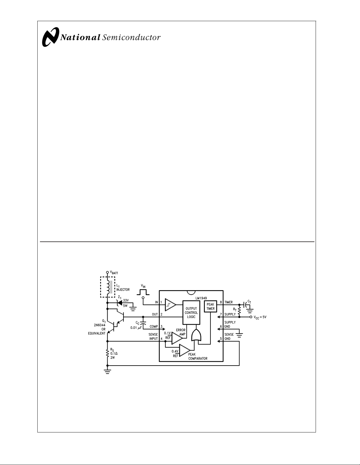
Typical Application Circuit
Features
n Low voltage supply (3V–5.5V)
n 22 mA output drive current
n No RFI radiation
n Adaptable to all injector current levels
n Highly accurate operation
n TTL/CMOS compatible input logic levels
n Short circuit protection
n High impedance input
n Externally set holding current, I
n Internally set peak current (4 x IH)
n Externally set time-out
n Can be modified for full switching operation
n Available in plastic 8-pin minDIP
H
Applications
n Fuel injection
n Throttle body injection
n Solenoid controls
n Air and fluid valves
n DC motor drives
Order Number LM1949M or LM1949N
See NS Package Number M08A or N08E
FIGURE 1. Typical Application and Test Circuit
© 2001 National Semiconductor Corporation DS005062 www.national.com
00506201
Absolute Maximum Ratings (Note 1)
If Military/Aerospace specified devices are required,
LM1949
please contact the National Semiconductor Sales Office/
Distributors for availability and specifications.
Supply Voltage 8V
Input Voltage Range −0.3V to V
Operating Temperature Range −40˚C to +125˚C
Storage Temperature Range −65˚C to +150˚C
Junction Temperature 150˚C
Lead Temp. (Soldering 10 sec.) 260˚C
Power Dissipation (Note 2) 1235 mW
Electrical Characteristics
(VCC= 5.5V, VIN= 2.4V, TJ= 25˚C,
Symbol Parameter Conditions Min Typ Max Units
I
CC
Supply Current
Off V
Peak Pin 8 = 0V 28 54 mA
Hold Pin 8 Open 16 26 mA
V
OH
V
OL
I
B
I
OP
Input On Level VCC= 5.5V 1.4 2.4 V
Input Off Level VCC= 5.5V 1.0 1.35 V
Input Current −25 3 +25 µA
Output Current
Peak Pin 8 = 0V −10 −22 mA
Hold Pin 8 Open −1.5 −5 mA
V
S
Output Saturation Voltage 10 mA, VIN= 0V 0.2 0.4 V
Sense Input
V
P
V
H
Peak Threshold VCC= 4.75V 350 386 415 mV
Hold Reference 88 94 102 mV
t Time-out, t t ÷ R
Note 1: Absolute Maximum Ratings indicate limits beyond which damage to the device may occur.
Note 2: For operation in ambient temperatures above 25˚C, the device must be derated based on a 150˚C maximum junction temperature and a thermal resistance
of 100˚C/W junction to ambient.
Figure 1
, unless otherwise specified.)
=0V 11 23 mA
IN
V
= 3.0V 1.2 1.6 V
CC
V
= 3.0V 0.7 1.15 V
CC
TCT
90 100 110 %
CC
www.national.com 2
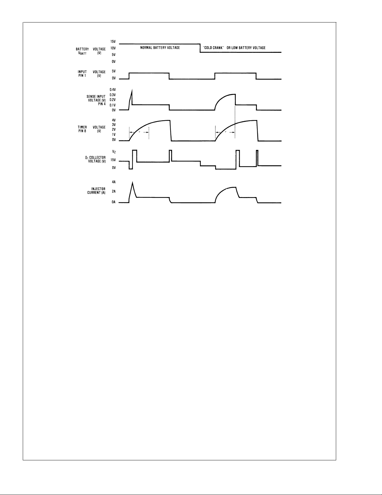
Typical Circuit Waveforms
LM1949
00506202
www.national.com3
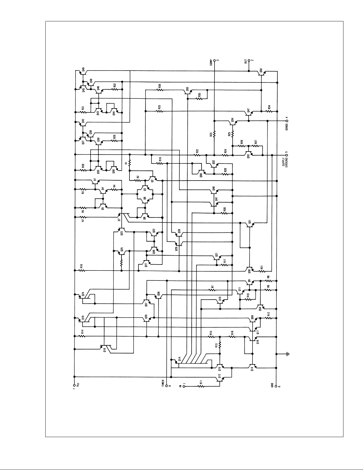
LM1949
00506203
FIGURE 2. LM1949 Circuit
Schematic Diagram
www.national.com 4

Typical Performance Characteristics
Quiescent Current vs
Supply Voltage
LM1949
Supply Current vs
Supply Voltage
Output Current vs
Supply Voltage
Sense Input Peak Voltage
vs Supply Voltage
00506225
00506211
Input Voltage Thresholds
vs Supply Voltage
00506212 00506213
Sense Input Hold Voltage
vs Supply Voltage
00506214
00506215
www.national.com5

Typical Performance Characteristics (Continued)
LM1949
Normalized Timer Function
vs Supply Voltage
Quiescent Supply Current
vs Junction Temperature
00506216
Quiescent Supply Current
vs Junction Temperature
00506217
Output Current vs
Junction Temperature
Input Voltage Thresholds
vs Junction Temperature
00506218
00506220
00506219
Sense Input Peak Voltage
vs Junction Temperature
00506204
www.national.com 6

Typical Performance Characteristics (Continued)
LM1949
Sense Input Hold Voltage
vs Junction Temperature
LM1949N Junction
Temperature Rise Above
Ambient vs Supply Voltage
00506221
Normalized Timer Function
vs Junction Temperature
00506222
00506205
Application Hints
The injector driver integrated circuits were designed to be
used in conjunction with an external controller. The LM1949
derives its input signal from either a control oriented processor (COPS
input signal, in the form of a square wave with a variable duty
cycle and/or variable frequency, is applied to Pin 1. In a
typical system, input frequency is proportional to engine
RPM. Duty cycle is proportional to the engine load. The
circuits discussed are suitable for use in either open or
closed loop systems. In closed loop systems, the engine
exhaust is monitored and the air-to-fuel mixture is varied (via
the duty cycle) to maintain a perfect, or stochiometric, ratio.
INJECTORS
Injectors and solenoids are available in a vast array of sizes
and characteristics. Therefore, it is necessary to be able to
design a drive system to suit each type of solenoid. The
purpose of this section is to enable any system designer to
use and modify the LM1949 and associated circuitry to meet
the system specifications.
Fuel injectors can usually be modeled by a simple RL circuit.
Figure 3
actual operation, the value of L
™
), microprocessor, or some other system. This
shows such a model for a typical fuel injector. In
will depend upon the status
1
of the solenoid. In other words, L
will change depending
1
upon whether the solenoid is open or closed. This effect, if
pronounced enough, can be a valuable aid in determining
the current necessary to open a particular type of injector.
The change in inductance manifests itself as a breakpoint in
the initial rise of solenoid current. The waveforms on Page 2
at the sense input show this occurring at approximately 130
mV. Thus, the current necessary to overcome the constrictive forces of that particular injector is 1.3 amperes.
00506206
FIGURE 3. Model of a Typical Fuel Injector
PEAK AND HOLD CURRENTS
The peak and hold currents are determined by the value of
the sense resistor R
1 signal at Pin 1, initially drives Darlington transistor Q
. The driver IC, when initiated by a logic
S
1
into
saturation. The injector current will rise exponentially from
zero at a rate dependent upon L
and the saturation voltage of Q
1
, the battery voltage
1,R1
. The drop across the sense
www.national.com7

Application Hints (Continued)
resistor is created by the solenoid current, and when this
LM1949
drop reaches the peak threshold level, typically 385 mV, the
IC is tripped from the peak state into the hold state. The IC
now behaves more as an op amp and drives Q
closed loop system to maintain the hold reference voltage,
typically 94 mV, across R
from the peak level to the hold level, it remains there for the
duration of the input signal at Pin 1. This mode of operation
is preferable when working with solenoids, since the current
required to overcome kinetic and constriction forces is often
a factor of four or more times the current necessary to hold
the injector open. By holding the injector current at one
fourth of the peak current, power dissipation in the solenoids
and Q
In the circuit of
is reduced by at least the same factor.
1
Figure 1
shown opens when the current exceeds 1.3 amps and
closes when the current then falls below 0.3 amps. In order
to guarantee injector operation over the life and temperature
range of the system, a peak current of approximately 4 amps
was chosen. This led to a value of R
peak and hold thresholds by this factor gives peak and hold
currents through the solenoid of 3.85 amps and 0.94 amps
respectively.
Different types of solenoids may require different values of
current. The sense resistor R
An 8-amp peak injector would use R
Note that for large currents above one amp, IR drops within
the component leads or printed circuit board may create
substantial errors unless appropriate care is taken. The
sense input and sense ground leads (Pins 4 and 5 respectively), should be Kelvin connected to R
should not be allowed to flow through any part of these
traces or connections. An easy solution to this problem on
double-sided PC boards (without plated-through holes) is to
have the high current trace and sense trace attach to the R
lead from opposite sides of the board.
TIMER FUNCTION
The purpose of the timer function is to limit the power dissipated by the injector or solenoid under certain conditions.
Specifically, when the battery voltage is low due to engine
cranking, or just undercharged, there may not be sufficient
voltage available for the injector to achieve the peak current.
In the
Figure 2
waveforms under the low battery condition,
the injector current can be seen to be leveling out at 3 amps,
or 1 amp below the normal threshold. Since continuous
operation at 3 amps may overheat the injectors, the timer
function on the IC will force the transition into the hold state
after one time constant (the time constant is equal to R
The timer is reset at the end of each input pulse. For systems
where the timer function is not needed, it can be disabled by
grounding Pin 8. For systems where the initial peak state is
not required, (i.e., where the solenoid current rises immediately to the hold level), the timer can be used to disable the
peak function. This is done by setting the time constant
equal to zero, (i.e., C
mended. The timer will then complete its time-out and disable the peak condition before the solenoid current has had
a chance to rise above the hold level.
The actual range of the timer in injection systems will probably never vary much from the 3.9 milliseconds shown in
Figure 1
. However, the actual useful range of the timer
extends from microseconds to seconds, depending on the
component values chosen. The useful range of R
. Once the injector current drops
S
, it was known that the type of injector
of 0.1Ω. Dividing the
S
may be changed accordingly.
S
= 0). Leaving RTin place is recom-
T
equal to .05Ω, etc.
S
. High current
S
within a
1
T
TCT
is ap-
proximately 1k to 240k. The capacitor C
is limited only by
T
stray capacitances for low values and by leakages for large
values.
The capacitor reset time at the end of each controller pulse
is determined by the supply voltage and the capacitor value.
The IC resets the capacitor to an initial voltage (V
BE
)by
discharging it with a current of approximately 15 mA. Thus, a
0.1 µF cap is reset in approximately 25 µs.
COMPENSATION
Compensation of the error amplifier provides stability for the
circuit during the hold state. External compensation (from
Pin 2 to Pin 3) allows each design to be tailored for the
characteristics of the system and/or type of Darlington power
device used. In the vast majority of designs, the value or type
of the compensation capacitor is not critical. Values of 100
pF to 0.1 µF work well with the circuit of
Figure 1
. The value
shown of 0.1 µF (disc) provides a close optimum in choice
between economy, speed, and noise immunity. In some
systems, increased phase and gain margin may be acquired
by bypassing the collector of Q
to ground with an appropri-
1
ately rated 0.1 µF capacitor. This is, however, rarely necessary.
FLYBACK ZENER
The purpose of zener Z
tive, a voltage spike is produced at the collector of Q
is twofold. Since the load is induc-
1
1
anytime the injector is reduced. This occurs at the
peak-to-hold transition, (when the current is reduced to one
fourth of its peak value), and also at the end of each input
pulse, (when the current is reduced to zero). The zener
provides a current path for the inductive kickback, limiting
the voltage spike to the zener value and preventing Q
1
from
damaging voltage levels. Thus, the rated zener voltage at
the system peak current must be less than the guaranteed
minimum breakdown of Q
S
ing the majority of the injector current during the
peak-to-hold transition (see
. Also, even while Z1is conduct-
1
Figure 4
), Q1is operating at the
hold current level. This fact is easily overlooked and, as
described in the following text, can be corrected if necessary.
Since the error amplifier in the IC demands 94 mV across
R
will be biased to provide exactly that. Thus, the safe
S,Q1
operating area (SOA) of Q
with a V
of Z1volts. For systems where this is not desired,
CE
the zener anode may be reconnected to the top of R
shown in
Figure 5
. Since the voltage across the sense
must include the hold current
1
as
S
resistor now accurately portrays the injector current at all
times, the error amplifier keeps Q
off until the injector
1
current has decayed to the proper value. The disadvantage
of this particular configuration is that the ungrounded zener
).
is more difficult to heat sink if that becomes necessary.
The second purpose of Z
is to provide system transient
1
protection. Automotive systems are susceptible to a vast
array of voltage transients on the battery line. Though their
duration is usually only milliseconds long, Q
permanent damage unless buffered by the injector and Z
could suffer
1
.
1
There is one reason why a zener is preferred over a clamp
diode back to the battery line, the other reason being long
decay times.
www.national.com 8

Application Hints (Continued)
discontinuities and breakpoints in the power waveforms of
the various components, most notably at the peak-to-hold
transition. Some generalizations can be made for normal
operation. For example, in a typical cycle of operation, the
majority of dissipation occurs during the hold state. The hold
state is usually much longer than the peak state, and in the
peak state nearly all power is stored as energy in the magnetic field of the injector, later to be dumped mostly through
the zener. While this assumption is less accurate in the case
of low battery voltage, it nevertheless gives an unexpectedly
accurate set of approximations for general operation.
Figure 1
The following nomenclature refers to
. Typical values
are given in parentheses:
R
= Sense Resistor (0, 1Ω)
S
V
= Sense Input Hold Voltage (.094V)
H
V
= Sense Input Peak Voltage (.385V)
P
V
=Z1Zener Breakdown Voltage (33V)
Z
V
= Battery Voltage (14V)
BATT
L
= Injector Inductance (.002H)
1
R
= Injector Resistance (1Ω)
1
n = Duty Cycle of Input Voltage of Pin 1 (0 to 1)
f = Frequency of Input (10 Hz to 200 Hz)
Power Dissipation:
Q
1
LM1949
00506207
FIGURE 4. Circuit Waveforms
00506208
FIGURE 5. Alternate Configuration for Zener Z
1
POWER DISSIPATION
The power dissipation of the system shown in
Figure 1
dependent upon several external factors, including the frequency and duty cycle of the input waveform to Pin 1.
Calculations are made more difficult since there are many
SWITCHING INJECTOR DRIVER CIRCUIT
The power dissipation of the system, and especially of Q
,
1
can be reduced by employing a switching injector driver
circuit. Since the injector load is mainly inductive, transistor
Q
can be rapidly switched on and off in a manner similar to
1
switching regulators. The solenoid inductance will naturally
integrate the voltage to produce the required injector current,
while the power consumed by Q
will be reduced. A note of
1
caution: The large amplitude switching voltages that are
present on the injector can and do generate a tremendous
amount of radio frequency interference (RFI). Because of
this, switching circuits are not recommended. The extra cost
of shielding can easily exceed the savings of reduced power.
In systems where switching circuits are mandatory, extensive field testing is required to guarantee that RFI cannot
create problems with engine control or entertainment equipment within the vicinity.
is
The LM1949 can be easily modified to function as a switcher.
Accomplished with the circuit of
components required are two external resistors, R
Figure 7
, the only additional
and RB.
A
Additionally, the zener needs to be reconnected, as shown,
www.national.com9

Application Hints (Continued)
to R
LM1949
. The amount of ripple on the hold current is easily
S
controlled by the resistor ratio of R
to RB.RBis kept small
A
so that sense input bias current (typically 0.3 mA) has negligible effect on V
. Duty cycle and frequency of oscillation
H
during the hold state are dependent on the injector characteristics, R
, and the zener voltage as shown in the
A,RB
following equations.
As shown, the power dissipation by Q1in this manner is
substantially reduced. Measurements made with a thermocouple on the bench indicated better than a fourfold reduction in power in Q
. However, the power dissipation of the
1
zener (which is independent of the zener voltage chosen) is
increased over the circuit of
Figure 1
.
00506209
FIGURE 6. Switching Waveforms
FIGURE 7. Switching Application Circuit
www.national.com 10
00506210

Physical Dimensions inches (millimeters) unless otherwise noted
LM1949
14-Lead (0.150" Wide) Molded Small Outline Package, JEDEC
Order Number LM1949M
NS Package Number M08A
www.national.com11

Physical Dimensions inches (millimeters) unless otherwise noted (Continued)
LM1949 Injector Drive Controller
Molded Dual-In-Line Package (N)
Order Number LM1949N
NS Package Number N08E
LIFE SUPPORT POLICY
NATIONAL’S PRODUCTS ARE NOT AUTHORIZED FOR USE AS CRITICAL COMPONENTS IN LIFE SUPPORT
DEVICES OR SYSTEMS WITHOUT THE EXPRESS WRITTEN APPROVAL OF THE PRESIDENT AND GENERAL
COUNSEL OF NATIONAL SEMICONDUCTOR CORPORATION. As used herein:
1. Life support devices or systems are devices or
systems which, (a) are intended for surgical implant
into the body, or (b) support or sustain life, and
whose failure to perform when properly used in
accordance with instructions for use provided in the
2. A critical component is any component of a life
support device or system whose failure to perform
can be reasonably expected to cause the failure of
the life support device or system, or to affect its
safety or effectiveness.
labeling, can be reasonably expected to result in a
significant injury to the user.
National Semiconductor
Corporation
Americas
Email: support@nsc.com
www.national.com
National does not assume any responsibility for use of any circuitry described, no circuit patent licenses are implied and National reserves the right at any time without notice to change said circuitry and specifications.
National Semiconductor
Europe
Fax: +49 (0) 180-530 85 86
Email: europe.support@nsc.com
Deutsch Tel: +49 (0) 69 9508 6208
English Tel: +44 (0) 870 24 0 2171
Français Tel: +33 (0) 1 41 91 8790
National Semiconductor
Asia Pacific Customer
Response Group
Tel: 65-2544466
Fax: 65-2504466
Email: ap.support@nsc.com
National Semiconductor
Japan Ltd.
Tel: 81-3-5639-7560
Fax: 81-3-5639-7507
 Loading...