


查询LM12434CIWM供应商
July 1995
LM12434/LM12
with Serial I/O and Self-Calibration
LM12434/LM12ÀLÓ438 12-Bit
a
Sign Data Acquisition
System with Serial I/O and Self-Calibration
General Description
The LM12434 and LM12ÀLÓ438 are highly integrated Data
Acquisition Systems. Operating on 3V to 5V, they combine a
fully-differential self-calibrating (correcting linearity and zero
errors) 13-bit (12-bit
(ADC) and sample-and-hold (S/H) with extensive analog
and digital functionality. Up to 32 consecutive conversions,
using two’s complement format, can be stored in an internal
32-word (16-bit wide) FIFO data buffer. An internal 8-word
instruction RAM can store the conversion sequence for up
to eight acquisitions through the LM12
multiplexer. The LM12434 has a four-channel multiplexer, a
differential multiplexer output, and a differential S/H input.
The LM12434 and LM12
a
sign resolution and in a supervisory ‘‘watchdog’’ mode
that compares an input signal against two programmable
limits.
Acquisition times and conversion rates are programmable
through the use of internal clock-driven timers. The differential reference voltage inputs can be externally driven for absolute or ratiometric operation.
All registers, RAM, and FIFO are directly accessible through
the high speed and flexible serial I/O interface bus. The
serial interface bus is user selectable to interface with the
following protocols with zero glue logic: MICROWIRE/
TM
PLUS
, Motorola’s SPI/QSPI, Hitachi’s SCI, 8051 Family’s
Serial Port (Mode 0), I
Port.
An evaluation kit for demonstrating the LM12434 and
ÀLÓ
LM12
438 is available.
TRI-STATEÉis a registered trademark of National Semiconductor Corporation.
MICROWIRE/PLUS
Windows
TM
is a registered trademark of Microsoft Corporation.
É
a
sign) analog-to-digital converter
ÀLÓ
438’s eight-input
ÀLÓ
438 can also operate with 8-bit
2
C and the TMS320 Family’s Serial
is a trademark of National Semiconductor Corporation.
Key Specifications
e
f
8 MHzÀL, f
CLK
Y
Resolution 12-bitasign or 8-bitasign
Y
13-bit conversion time 5.5 msÀ7.3 msÓ(max)
Y
9-bit conversion time 2.6 msÀ3.5 msÓ(max)
Y
13-bit Through-put rate
Y
Comparison time (‘‘watchdog’’ mode)
Y
Serial Clock 10 MHzÀ6 MHzÓ(max)
Y
Integral Linearity Error
Y
VINrange GND to V
Y
Power dissipation 45 mWÀ20 mWÓ(max)
Y
Stand-by mode
power dissipation 25 mW
Y
Supply voltage LM12L438 3.3Vg10%
Features
Y
Three operating modes: 12-bitasign, 8-bitasign,
and ‘‘watchdog’’ comparison mode
Y
Single-ended or differential inputs
Y
Built-in Sample-and-Hold
Y
Instruction RAM and event sequencer
Y
8-channel (LM12ÀLÓ438) or 4-channel (LM12434)
multiplexer
Y
32-word conversion FIFO
Y
Programmable acquisition times and conversion rates
Y
Self-calibration and diagnostic mode
Y
Power down output for system power management
Y
Read while convert capability for maximum through-put
e
CLK
140k samples/s
LM12434/8 5V
rate
Applications
Y
Data Logging
Y
Portable Instrumentation
Y
Process Control
Y
Energy Management
Y
Robotics
6 MHz
Ó
À
105k sample/sÓ(min)
À
1.4 ms
1.8 msÓ(max)
g
1 LSB (max)
À
16.5 mWÓ(typ)
g
A
10%
À
L
Ó
438 12-Bit
a
a
Sign Data Acquisition System
Connection Diagrams
28-Pin PLCC Package
*Pin names in ( ) apply to the LM12434
TL/H/11879– 1
Order Number LM12434CIWM, LM12438CIWM, or
Order Number LM12434CIV, LM12438CIV, or
LM12L438CIV
See NS Package Number V28A
C
1995 National Semiconductor Corporation RRD-B30M85/Printed in U. S. A.
TL/H/11879
28-Pin Wide Body SO Package
TL/H/11879– 2
LM12L438CIWM
See NS Package Number M28B

Table of Contents
1.0 FUNCTIONAL DIAGRAMS АААААААААААААААААААААААА3
2.0 ELECTRICAL SPECIFICATIONS АААААААААААААААААА5
2.1 Ratings ААААААААААААААААААААААААААААААААААААААА5
2.1.1 Absolute Maximum Ratings ААААААААААААААААА5
2.1.2 Operating Ratings ААААААААААААААААААААААААА5
2.2 Performance Characteristics ААААААААААААААААААААА5
2.2.1 Converter Static Characteristics ААААААААААААА5
2.2.2 Converter Dynamic Characteristics АААААААААА6
2.2.3 DC CharacteristicsААААААААААААААААААААААААА8
2.2.4 Digital DC CharacteristicsААААААААААААААААААА9
2.3 Digital Switching Characteristics ААААААААААААААААА10
2.3.1 Standard Interface Mode АААААААААААААААААА10
2.3.2 8051 Interface ModeАААААААААААААААААААААА11
2.3.3 TMS320 Interface ModeААААААААААААААААААА12
2
2.3.4 I
C Bus Interface ААААААААААААААААААААААААА13
2.4 Notes on Specifications АААААААААААААААААААААААА14
3.0 ELECTRICAL CHARACTERISTICS ААААААААААААААА15
4.0 TYPICAL PERFORMANCE CHARACTERISTICS ÀÀÀ19
5.0 PIN DESCRIPTIONS АААААААААААААААААААААААААААА23
6.0 OPERATIONAL INFORMATION АААААААААААААААААА27
6.1 Functional Description ААААААААААААААААААААААААА27
6.2 Internal User-Accessible Registers АААААААААААААА31
6.2.1 Instruction RAM АААААААААААААААААААААААААА31
6.2.2 Configuration Register АААААААААААААААААААА38
6.2.3 InterruptsАААААААААААААААААААААААААААААААА38
6.2.4 Interrupt Enable Register АААААААААААААААААА39
6.2.5 Interrupt Status Register АААААААААААААААААА39
6.2.6 Limit Status Register АААААААААААААААААААААА40
6.2.7 Timer ААААААААААААААААААААААААААААААААААА40
6.2.8 FIFOАААААААААААААААААААААААААААААААААААА40
6.3 Instruction SequencerАААААААААААААААААААААААААА41
7.0 DIGITAL INTERFACE ААААААААААААААААААААААААААА43
7.1 Standard Interface Mode ААААААААААААААААААААААА43
7.1.1 Examples of Interfacing to the HPC 46XXX’s
MICROWIRE/PLUS
TM
and 68HC11’s SPI ÀÀÀ50
7.2 8051 Interface ModeААААААААААААААААААААААААААА59
7.2.1 Example of Interfacing to the 8051АААААААААА62
7.3 TMS320 Interface ModeАААААААААААААААААААААААА66
7.3.1 Example of Interfacing to the TMS320C3x ÀÀÀ69
2
7.4 I
C Bus Interface АААААААААААААААААААААААААААААА74
7.4.1 Example of Interfacing to an I
2
C ControllerÀÀÀ76
8.0 ANALOG CONSIDERATIONS АААААААААААААААААААА77
8.1 Reference Voltage АААААААААААААААААААААААААААА77
8.2 Input Range АААААААААААААААААААААААААААААААААА77
8.3 Input Current ААААААААААААААААААААААААААААААААА77
8.4 Input Source Resistance ААААААААААААААААААААААА77
8.5 Input Bypass Capacitance АААААААААААААААААААААА77
8.6 Input Noise ААААААААААААААААААААААААААААААААААА77
8.7 Power Supply Consideration АААААААААААААААААААА77
8.8 PC Board Layout and Grounding ConsiderationÀÀÀÀ78
2

1.0 Functional Diagrams
LM12434
INTERFACE MODESEL1 MODESEL2 P1 P2 P3 P4 P5
Standard 0 1 R
8051 0 0 1* 1* CS RXD TXD
I2C 1 0 SAD0 SAD1 SAD2 SDA SCL
TMS320 1 1 FSR FSX DX DR SCLK
*Internal pull-up
/F CS
DI DO SCLK
Ordering Information (LM12434)
Part Number Package Type NSC Package Number Temperature Range
LM12434CIV 28-Pin PLCC V28A
LM12434CIWM 28-Pin Wide Body SO M28B
3
b
40§Ctoa85§C
b
40§Ctoa85§C
TL/H/11879– 3
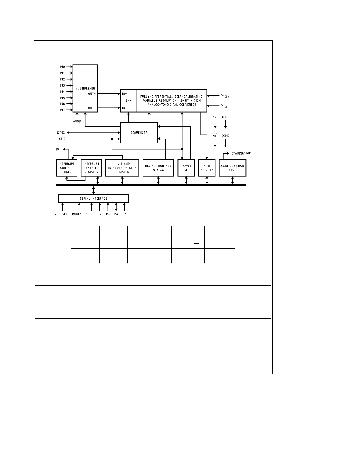
1.0 Functional Diagrams (Continued)
LM12
ÀLÓ
438
INTERFACE MODESEL1 MODESEL2 P1 P2 P3 P4 P5
Standard 0 1 R/F CS DI DO SCLK
8051 0 0 1* 1* CS RXD TXD
I2C 1 0 SAD0 SAD1 SAD2 SDA SCL
TMS320 1 1 FSR FSX DX DR SCLK
*Internal pull-up
Ordering Information (LM12ÀLÓ438)
Part Number Package Type NSC Package Number Temperature Range
LM12438CIV 28-Pin PLCC V28A
LM12L438CIV
LM12438CIWM 28-Pin Wide Body SO M28B
LM12L438CIWM
LM12438 Eval Evaluation Board and WindowsÉbased software
4
b
40§Ctoa85§C
b
40§Ctoa85§C
TL/H/11879– 4

2.0 Electrical Specifications
2.1 RATINGS
2.1.1 Absolute Maximum Ratings (Notes1&2)
If Military/Aerospace specified devices are required,
please contact the National Semiconductor Sales
Office/Distributors for availability and specifications.
Supply Voltage (V
a
A
Voltage at Input and Output Pins
except IN0–IN3 (LM12434)
and IN0 – IN7 (LM12
Voltage at Analog Inputs IN0– IN3 (LM12434)
and IN0–IN7 (LM12
a
a
b
V
V
l
A
AGNDbDGND
l
l
D
l
Input Current at Any Pin (Note 3)
Package Input Current (Note 3)
Power Dissipation (T
V Package
a
and V
) 6.0V
D
ÀLÓ
438)
ÀLÓ
438) GNDb5V to V
e
25§C) (Note 4)
A
b
0.3V to V
a
a
a
300 mV
300 mV
g
g
0.3V
a
5V
5mA
20 mA
WM Package
Storage Temperature
b
65§Ctoa150§C
Soldering Information, Lead Temperature (Note 19)
V Package, Vapor Phase (60 seconds)
Infrared (15 seconds)
WM Package, Vapor Phase (60 seconds)
Infrared (15 seconds)
ESD Susceptibility (Note 5) 1.5 kV
2.2 PERFORMANCE CHARACTERISTICS All specifications apply to the LM12434, LM12438, and LM12L438 unless otherwise
noted. Specifications in braces
2.2.1 Converter Static Characteristics The following specifications apply to the LM12434 and LM12
a
e5VÀ
V
D
8.0 MHzÀ6 MHzÓ,R
À
1.25VÓcommon-mode voltage, and minimum acquisition time unless otherwise specified. Boldface limits apply for T
T
J
3.3VÓ, AGNDeDGNDe0V, V
e
T
to T
MIN
MAX
ÀÓ
apply only to the LM12L438.
e
25X, source impedance for V
S
; all other limits T
e
T
A
e
4.096VÀ2.5VÓ,V
a
REF
e
25§C. (Notes 6, 7, 8 and 9)
J
Symbol Parameter Conditions
ILE Positive and Negative Integral After Auto-Cal (Notes 12, 17)
Linearity Error
TUE Total Unadjusted Error After Auto-Cal (Note 12)
Resolution with No Missing Codes After Auto-Cal (Note 12) 13 Bits
DNL Differential Non-Linearity After Auto-Cal
Zero Error After Auto-Cal (Notes 13, 17)
Positive Full-Scale Error After Auto-Cal (Notes 12, 17)
Negative Full-Scale Error After Auto-Cal (Notes 12, 17)
DC Common Mode Error (Note 14)
ILE 8-BitaSign and ‘‘Watchdog’’ (Note 12)
Mode Positive and Negative
Integral Linearity Error
TUE 8-BitaSign and ‘‘Watchdog’’ Mode After Auto-Zero
Total Unadjusted Error
8-BitaSign and ‘‘Watchdog’’ Mode
Resolution with No Missing Codes
2.1.2 Operating Ratings (Notes1&2)
Temperature Range (T
LM12434CIV/LM12
ÀLÓ
LM12434CIWM, LM12
Supply Voltage
a
a
V
,V
A
D
a
a
b
V
V
l
A
AGDNDbDGND
l
l
D
l
Analog Inputs Range GND
V
Input Voltage 1VsV
a
REF
V
Input Voltage 0VsV
b
REF
b
REF
a
V
V
and V
V
a
REF
Common Mode
REF
Range (Note 16) 0.1 V
REF
REF
b
REF
e
0V, 12-bitasign conversion mode, f
b
s
25X, fully-differential input with fixed 2.048V
b
Typical Limits Units
(Note 10) (Note 11) (Limit)
g
g
g
s
T
min
438CIV
ÀLÓ
438CIWMb40§CsT
b
40§CsT
3.0V to 5.5V
s
V
IN
REF
s
V
b
REF
a
s
A
0.35
g
1 LSB
g
0.2
g
0.2
g
0.2
g
0.2
g
2
0.15
1/2
g
g
g
g
g
g
À
g
g
g
REF
1VsV
REF
s
V
REFCM
ÀLÓ
438 for V
1 LSB (max)
1 LSB (max)
1 LSB (max)
2 LSB (max)
2 LSB (max)
3.5 LSB (max)
Ó
4.0
1/2 LSB (max)
1/2 LSB (max)
9 Bits (max)
A
s
s
a
a
s
A
A
a
0.6 V
T
max
s
85§C
s
85§C
100 mV
100 mV
s
V
s
V
b
s
V
a
A
CLK
A
)
a
A
a
A
1V
a
A
a
A
e
e
e
5

2.0 Electrical Specifications (Continued)
2.2.1 Converter Static Characteristics The following specifications apply to the LM12434 and LM12
a
e5VÀ
V
D
8.0 MHzÀ6 MHzÓ,R
À
1.25VÓcommon-mode voltage, and minimum acquisition time unless otherwise specified. Boldface limits apply for T
e
T
J
3.3VÓ, AGNDeDGNDe0V, V
T
to T
MIN
e
25X, source impedance for V
S
; all other limits T
MAX
e
A
Symbol Parameter Conditions
DNL 8-BitaSign and ‘‘Watchdog’’ Mode
Differential Non-Linearity
8-BitaSign and ‘‘Watchdog’’ Mode After Auto-Zero
Zero Error
e
4.096VÀ2.5VÓ,V
a
REF
e
T
25§C. (Notes 6, 7, 8 and 9) (Continued)
J
REF
a
and V
REF
REF
b
e
0V, 12-bitasign conversion mode, f
b
s
25X, fully-differential input with fixed 2.048V
Typical Limits Units
(Note 10) (Note 11) (Limit)
g
g
8-BitaSign and ‘‘Watchdog’’ Positive
and Negative Full-Scale Error
8-BitaSign and ‘‘Watchdog’’ Mode
DC Common Mode Error
Multiplexer Channel-to-Channel
Matching
V
a
IN
V
b
IN
b
V
a
IN
b
V
a
IN
Non-Inverting GND V (min)
Input Range
Inverting GND V (min)
Input Range
V
Differential Input Voltage Range
b
IN
V
Common Mode Input Voltage Range GND V (min)
b
IN
g
g
2
a
a
e
PSS Power Supply Zero Error V
Sensitivity Full-Scale Error V
(Note 15) Linearity Error
C
REF
C
IN
2.2.2 Converter Dynamic Characteristics The following specifications apply only to the LM12434 and LM12438 for V
a
V
D
throughput rate
2.048V
for T
V
/V
REF
a
Input Capacitance 85 pF
b
REF
Selected Multiplexer Channel Input
Capacitance
e
5V, AGNDeDGNDe0V, V
e
T
J
133.3 kHz, R
e
T
MIN
to T
À
1.25VÓcommon-mode voltage, and minimum acquisition time unless otherwise specified. Boldface limits apply
e
A
e
S
; all other limits T
MAX
e
a
REF
25X, source impedance for V
4.096V, V
e
T
A
J
A
REF
REF
e
25§C. (Notes 6, 7, 8 and 9)
Symbol Parameter Conditions
e
V
5Vg10%,
D
e
4.096V, V
a
e
0V, 12-bitasign conversion mode, f
b
REF
a
and V
REF
REF
e
b
b
Typical Limits Units
(Note 10) (Note 11) (Limit)
g
GNDg0.25
s
25X, fully-differential input with fixed
CLK Duty Cycle 50 %
40 % (min)
60 % (max)
t
C
t
A
Conversion Time 13-Bit Resolution,
Sequencer State S5
9-Bit Resolution,
Sequencer State S5
Acquisition Time Sequencer State S7
(Figure 10)
(Figure 10)
(Figure 10)
44 (t
21 (t
(Programmable) Minimum for 13-Bits 9 (t
Maximum for 13-Bits (D
Minimum for 9-Bits
e
15) 39 (t
(Figure 10)
2(t
Maximum for 9-Bits (De15) 2 (t
) 44 (t
CLK
) 21 (t
CLK
) 9(t
CLK
) 39 (t
CLK
) 2(t
CLK
) 32 (t
CLK
)a50 ns (max)
CLK
)a50 ns (max)
CLK
)a50 ns (max)
CLK
)a50 ns (max)
CLK
)a50 ns (max)
CLK
)a50 ns (max)
CLK
ÀLÓ
438 for V
0.1
g
1/2 LSB (max)
g
1/2 LSB (max)
g
1/2 LSB (max)
0.15
0.05
g
1/8 LSB
0.05 LSB
a
V
A
a
V
A
a
b
V
A
a
V
A
a
V
A
0.05
g
g
1.0 LSB (max)
g
1.5 LSB (max)
0.2 LSB
75 pF
CLK
e
t
CLK
A
CLK
V (max)
V (max)
V (min)
V (max)
V (max)
A
e
8.0 MHz,
CLK Period
a
e
e
e
A
a
e
6

2.0 Electrical Specifications (Continued)
2.2.2 Converter Dynamic Characteristics The following specifications apply only to the LM12434 and LM12438 for V
a
e
V
5V, AGNDeDGNDe0V, V
D
throughput rate
2.048V common-mode voltage, and minimum acquisition time unless otherwise specified. Boldface limits apply for T
e
T
T
J
MIN
to T
e
MAX
133.3 kHz, R
; all other limits T
e
25X, source impedance for V
S
Symbol Parameter Conditions
t
t
Auto-Zero Time Sequencer State S2
Z
Full Calibration Time Sequencer State S2
CAL
Throughput Rate (Note 18)
t
‘‘Watchdog’’ Mode Comparison Time Sequencer States S6, S4,
WD
SNR Signal-to-Noise Ratio, V
Differential Input f
SNR Signal-to-Noise Ratio, V
Single-Ended Input f
SINAD Signal-to-NoiseaDistortion Ratio, V
Differential Input f
SINAD Signal-to-NoiseaDistortion Ratio, V
Single-Ended Input f
THD Total Harmonic Distortion, V
Differential Input f
THD Total Harmonic Distortion, V
Distortion, Single-Ended Input f
ENOB Effective Number of Bits, V
Differential Input f
ENOB Effective Number of Bits, V
Single-Ended Input f
SFDR Spurious Free Dynamic Range, V
Differential Input f
SFDR Spurious Free Dynamic Range, V
Single-Ended Input f
A
REF
e
4.096V, V
a
e
e
T
25§C. (Notes 6, 7, 8 and 9) (Continued)
J
REF
e
b
REF
(Figure 10)
(Figure 10)
(Figure 10)
and S5
e
g
4.096V (Note 20)
IN
e
1 kHz 79 dB
IN
e
f
10 kHz 79 dB
IN
e
f
62 kHz 70 dB
IN
e
4.096 V
IN
e
IN
e
f
IN
e
f
IN
e
IN
e
IN
e
f
IN
e
f
IN
e
IN
e
IN
e
f
IN
e
f
IN
e
IN
e
IN
e
f
IN
e
f
IN
e
IN
e
IN
e
f
IN
e
f
IN
e
IN
e
IN
e
f
IN
e
f
IN
e
IN
e
IN
e
f
IN
e
f
IN
e
IN
e
IN
e
f
IN
e
f
IN
e
IN
e
IN
e
f
IN
e
f
IN
p-p
1 kHz 71 dB
10 kHz 71 dB
62 kHz 67 dB
g
4.096V (Note 20)
1 kHz 79 dB
10 kHz 78 dB
62 kHz 67 dB
4.096 V
p-p
1 kHz 71 dB
10 kHz 70 dB
62 kHz 64 dB
g
4.096V (Note 20)
1 kHz
10 kHz
62 kHz
4.096 V
p-p
1 kHz
10 kHz
62 kHz
g
4.096V (Note 20)
1 kHz 12.6 Bits
10 kHz 12.2 Bits
62 kHz 12.1 Bits
4.096 V
p-p
1 kHz 11.3 Bits
10 kHz 11.2 Bits
62 kHz 10.8 Bits
g
4.096V (Note 20)
1 kHz 90 dBc
10 kHz 86 dBc
62 kHz 76 dBc
4.096V V
1 kHz 90 dBc
p-p
10 kHz 85 dBc
62 kHz 72 dBc
0V, 12-bitasign conversion mode, f
and V
a
s
25X, fully-differential input with fixed
b
REF
Typical Limits Units
(Note 10) (Note 11) (Limit)
76 (t
4944 (t
) 76 (t
CLK
) 4944 (t
CLK
)a50 ns (max)
CLK
CLK
142 140
11 (t
) 11 (t
CLK
b
90 dBc
b
85 dBc
b
71 dBc
b
88 dBc
b
82 dBc
b
67 dBc
)a50 ns (max)
CLK
e
CLK
)a50 ns (max)
a
A
8.0 MHz,
A
kHz
(min)
e
e
7

2.0 Electrical Specifications (Continued)
2.2.2 Converter Dynamic Characteristics The following specifications apply only to the LM12434 and LM12438 for V
a
e
V
5V, AGNDeDGNDe0V, V
D
throughput rate
2.048V common-mode voltage, and minimum acquisition time unless otherwise specified. Boldface limits apply for T
e
T
T
J
MIN
to T
e
MAX
133.3 kHz, R
; all other limits T
e
S
Symbol Parameter Conditions
IMD Two Tone Intermodulation Distortion V
Differential Input f
IMD Two Tone Intermodulation Distortion V
Single Ended Input f
Multiplexer Channel-to-Channel Crosstalk V
t
PU
t
WU
2.2.3 DC Characteristics The following specifications apply to the LM12434 and LM12ÀLÓ438 for V
AGND
otherwise specified. Boldface limits apply for T
Power-Up Time 10 ms
Wake-Up Time (Note 22) 2 ms
e
DGNDe0V, V
REF
a
e
4.096VÀ2.5VÓ,V
and 8)
Symbol Parameter Conditions
a
I
D
a
I
A
I
ST
a
V
Supply Current f
D
a
V
Supply Current f
A
Stand-By Supply Current (I
D
Multiplexer ON-Channel Leakage Current V
Multiplexer OFF-Channel Leakage Current V
e
4.096V, V
a
REF
25X, source impedance for V
e
e
T
A
25§C. (Notes 6, 7, 8 and 9) (Continued)
J
b
REF
e
IN
e
19.190 kHz
1
e
f
19.482 kHz
2
e
IN
e
19.190 kHz
1
e
f
19.482 kHz
2
e
IN
e
f
IN
f
CROSSTALK
LM12434 MUXOUT Only
and LM12438 MUX
plus Converter (Note 21)
e
0V, f
b
REF
e
e
T
A
a
a
a
I
) Stand-By Mode Selected
A
T
J
e
8 MHzÀ6 MHz
CLK
e
f
SCLK
e
f
SCLK
e
8 MHzÀ6 MHz
CLK
e
f
SCLK
e
f
Stopped 5À5
CLK
e
f
8 MHzÀ6 MHz
CLK
e
f
SCLK
e
f
Stopped 1.4À0.8
CLK
e
f
8 MHzÀ6 MHz
CLK
a
e
5.5V
A
ON-Channel
OFF-Channel
ON-Channel
OFF-Channel
a
e
5.5VÀ3.3V
A
ON-Channele5.5VÀ3.3V
OFF-Channele0V 0.1 1.0À3.0ÓmA (max)
ON-Channel
OFF-Channel
e
0V, 12-bitasign conversion mode, f
and V
a
REF
s
25X, fully-differential input with fixed
b
REF
CLK
Typical Limits Units
(Note 10) (Note 11) (Limit)
g
4.096V (Note 20)
4.096 V
pp
4.096 V
PP
5 kHz
e
40 kHz
e
8.0 MHzÀ6 MHzÓand minimum acquisition time unless
CLK
to T
MIN
; all other limits T
MAX
b
82 dBc
b
80 dBc
b
90 dBc
a
e
V
A
D
e
e
T
A
25§C. (Notes 6, 7
J
Typical Limits Units
(Note 10) (Note 11) (Limit)
Ó
Stopped 2.0À1.4
10 MHzÀ8 MHz
Ó
Ó
4.0À2.0
2.8À2.2
Ó
Ó
5.0À2.5ÓmA (max)
Ó
4.0À3.5ÓmA (max)
Stopped
Ó
10 MHzÀ8 MHz
e
e
e
e
e
e
Ó
Ó
5.5V
0V 0.1 1.0À3.0ÓmA (max)
0V
5.5V 1.0À3.0ÓmA (max)
Ó
Ó
0V
5.5VÀ3.3V
Ó
120À50
1.4À0.8
Ó
Ó
Ó
Ó
1.0À3.0ÓmA (max)
a
e
e5VÀ
a
A
8.0 MHz,
A
3.3V],
mA (max)
mA (max)
mA (max)
mA (max)
mA (max)
e
e
8

2.0 Electrical Specifications (Continued)
2.2.3 DC Characteristics The following specifications apply to the LM12434 and LM12
e
AGND
DGNDe0V, V
otherwise specified. Boldface limits apply for T
and 8) (Continued)
REF
a
e
4.096VÀ2.5VÓ,V
REF
A
e
b
e
T
J
0V, f
e
e
8.0 MHzÀ6 MHzÓand minimum acquisition time unless
CLK
T
to T
MIN
MAX
Symbol Parameter Conditions
R
ON
Multiplexer ON-Resistance LM12434
e
V
5V 650 1000 X(max)
IN
e
V
2.5V 700 1000 X(max)
IN
e
V
0V 630 1000 X(max)
IN
ÀLÓ
438 for V
; all other limits T
Typical Limits Units
(Note 10) (Note 11) (Limit)
Multiplexer Channel-to-Channel LM12434
R
matching V
ON
2.2.4 Digital DC Characteristics The following specifications apply to the LM12434 and LM12ÀLÓ438 for V
À
3.3VÓ, AGNDeDGNDe0V, unless otherwise specified. Boldface limits apply for T
e
limits T
e
T
A
25§C. (Notes 6, 7 and 8)
J
e
5V
IN
e
V
2.5V
IN
e
V
0V
IN
Symbol Parameter Conditions
a
a
e
V
IN(1)
V
IN(0)
I
IN(1)
I
IN(0)
C
IN
V
OUT(1)
V
OUT(0)
I
OUT
Logical ‘‘1’’ Input Voltage V
Logical ‘‘0’’ Input Voltage V
Logical ‘‘1’’ Input Current V
Logical ‘‘0’’ Input Current V
A
a
A
IN
IN
All Digital Inputs 6 pF
Logical ‘‘1’’ Output Voltage V
Logical ‘‘0’’ Output Voltage V
TRI-STATEÉOutput Leakage Current V
I
OUT
I
OUT
I
OUT
V
a
A
a
A
OUT
OUT
e
V
5.5VÀ3.6V
D
a
e
e
V
4.5VÀ3.0V
D
e5VÀ
e
e
eb
eb
e
e
e
e5VÀ
Ó
3.3V
0V
a
e
V
4.5VÀ3.0V
D
360 mA 2.4 V (min)
10 mA 4.25À2.9
a
e
V
4.5VÀ3.0V
D
1.6 mA
0V
Ó
3.3V
g
1.0%
g
1.0%
g
1.0%
A
Typical Limits Units
(Note 10) (Note 11) (Limit)
Ó
Ó
0.005 1.0 mA (max)
b
0.005
Ó
Ó
b
0.05
0.05 3.0 mA (max)
a
A
e
T
A
g
g
g
e
e
T
T
J
MIN
a
e
e5VÀ
V
D
e
25§C. (Notes 6, 7
J
3.3V],
3.0% (max)
3.0% (max)
3.0% (max)
a
a
e
e
V
A
D
to T
; all other
MAX
2.0 V (min)
0.8 V (max)
b
1.0 mA (max)
Ó
V (min)
0.4 V (max)
b
3.0 mA (max)
5V
9

2.0 Electrical Specifications (Continued)
2.3 DIGITAL SWITCHING CHARACTERISTICS The following specifications apply to the LM12434 and LM12
ae5VÀ
e
V
D
Boldface limits apply for T
2.3.1 Standard Mode Interface (MICROWIRE/PLUS
Symbol
(See
Figure
t
1
t
2
t
3
t
4
t
5
t
6
t
7
t
8
*CLK is the main clock input to the device, pin number 24 in PLCC package or pin number 2 in SO package.
3.3VÓ, AGNDeDGNDe0V, CL(load capacitance) on output linese80 pF unless otherwise specified.
Below) (Note 10) (Note 11) (Limit)
e
e
T
T
A
J
MIN
to T
, all other limits for T
MAX
TM
, SCI and SPI/QSPI)
Parameter Conditions
e
e
T
A
25§C. (Notes 6, 7, and 9)
J
Typical Limits Units
SCLK (Serial Clock) Period 100À125
CS Set-Up Time to First
Clock Transition
DI Valid Set-Up Time to Data
Capture Transition of SCLK
DI Valid Hold Time to Data
Capture Transition of SCLK
DO Hold Time from Data Shift
Transition of SCLK
À30Ó
25
0 ns (min)
40 ns (min)
À
70
120
CS Hold Time from Last SCLK
Transition in a Read or Write Cycle 25 ns (min)
(Excluding Burst Read Cycle)
CS Inactive to CS Active Again
3
SCLK Idle Time between the
End of the Command Byte
Transfer and the Start of the (min)*
3
Data Transfer in Read Cycles
ÀLÓ
Ó
Ó
438 for V
ns (min)
ns (min)
ns (max)
CLK Cycle
(min)*
CLK Cycle
a
A
TL/H/11879– 18
10

2.0 Electrical Specifications (Continued)
2.3 DIGITAL SWITCHING CHARACTERISTICS The following specifications apply to the LM12434 and LM12
ae5VÀ
e
V
D
Boldface limits apply for T
2.3.2 8051 Interface Mode
Symbol
(See
Figure
t
9
t
10
t
11
t
12
t
13
t
14
t
15
t
16
*CLK is the main clock input to the device, pin number 24 in PLCC package or pin number 2 in SO package.
3.3VÓ, AGNDeDGNDe0V, CL(load capacitance) on output linese80 pF unless otherwise specified.
Below) (Note 10) (Note 11) (Limit)
e
e
T
T
to T
A
J
MIN
, all other limits for T
MAX
Parameter Conditions
e
e
T
A
25§C. (Notes 6, 7, and 9) (Continued)
J
Typical Limits Units
TXD (Serial Clock Period) 125À250
CS Set-Up Time to First
Clock Transition
Data in Valid Set-Up Time to
TXD Clock High
Data in Valid Hold Time
from TXD Clock High
Data Out Hold Time
from TXD Clock High
À40Ó
25
40 ns (min)
À90Ó
40
À
70
120
CS Hold Time from Last TXD
High in a Read or Write Cycle 25À50
Ó
(Excluding Burst Read Cycle)
CS Inactive to CS Active Again
3
SCLK Idle Time between the
End of the Command Byte
Transfer and the Start of the (min)*
3
Data Transfer in Read Cycles
Ó
Ó
ÀLÓ
438 for V
ns (min)
ns (min)
ns (min)
ns (max)
ns (min)
CLK Cycle
(min)*
CLK Cycle
a
A
TL/H/11879– 21
11

2.0 Electrical Specifications (Continued)
2.3 DIGITAL SWITCHING CHARACTERISTICS The following specifications apply to the LM12434 and LM12
ae5VÀ
e
V
D
Boldface limits apply for T
2.3.3 TMS320 Interface Mode
Symbol
(See
Figure
t
22
t
23
t
24
t
25
t
26
t
27
t
28
t
29
3.3VÓ, AGNDeDGNDe0V, CL(load capacitance) on output linese80 pF unless otherwise specified.
Below) (Note 10) (Note 11) (Limit)
e
e
T
T
to T
A
J
MIN
, all other limits for T
MAX
Parameter Conditions
e
e
T
A
25§C. (Notes 6, 7, and 9) (Continued)
J
Typical Limits Units
SCLK (Serial Clock) Period 125À167
FSX Set-Up Time to SCLK High 30À50
FSX Hold Time from SCLK High 10 ns (min)
Data in (DX) Set-Up
Time to SCLK Low
Data in DX Hold Time from
SCLK Low
0 ns (min)
À
30
120
FSR High from SCLK High 80À100
FSR Low from SCLK Low 120 ns (max)
SCLK High to Data
Out (DR) Change
90 ns (max)
ÀLÓ
Ó
Ó
Ó
Ó
438 for V
ns (min)
ns (min)
ns (min)
ns (max)
a
A
TL/H/11879– 23
12

2.0 Electrical Specifications (Continued)
2.3 DIGITAL SWITCHING CHARACTERISTICS The following specifications apply to the LM12434 and LM12
ae5VÀ
e
V
D
Boldface limits apply for T
2
2.3.4 I
C Bus Interface
The switching characteristics of the LM12434/8 for I2C bus interface fully meets or exceeds the published specifications of the
2
I
C bus. The following parameters given here are the timing relationships between SCL and SDA signals related to the
LM12434/8. They are not the I
Symbol
(See
Figure
t
17
t
18
t
19
t
20
t
21
3.3VÓ, AGNDeDGNDe0V, CL(load capacitance) on output linese80 pF unless otherwise specified.
Below) (Note 10) (Note 11) (Limit)
e
e
T
T
to T
A
J
MIN
2
C bus specifications.
, all other limits for T
MAX
Parameter Conditions
e
e
T
A
25§C. (Notes 6, 7, and 9) (Continued)
J
Typical Limits Units
SCL (Clock) Period 2500À10000
Data in Set-Up Time to SCL High 30 ns (min)
Data Out Stable after SCL Low 900À1400
SDA Low Set-Up Time to SCL
Low (Start Condition)
SDA High Hold Time after SCL
High (Stop Condition)
ÀLÓ
438 for V
Ó
ns (min)
Ó
ns (max)
40 ns (min)
40 ns (min)
a
A
TL/H/11879– 22
13

2.0 Electrical Specifications (Continued)
2.4 NOTES ON SPECIFICATIONS
Note 1: Absolute Maximum Ratings indicate limits beyond which damage to the device may occur. Operating Ratings indicate conditions for which the device is
functional, but do not guarantee specific performance limits. For guaranteed specifications and test conditions, see the Electrical Characteristics. The guaranteed
specifications apply only for the test conditions listed. Some performance characteristics may degrade when the device is not operated under the listed test
conditions.
Note 2: All voltages are measured with respect to GND, unless otherwise specified. GND specifies either AGND and/or DGND and V
a
.
or V
D
Note 3: When the input voltage (V
5 mA. The 20 mA maximum package input current rating allows the voltage at any four pins, with an input current of 5 mA, to simultaneously exceed the power
supply voltages.
Note 4: The maximum power dissipation must be derated at elevated temperatures and is dictated by T
junction to ambient thermal resistance), and T
or the number given in the Absolute Maximum Ratings, whichever is lower. For this device, T
H
JA
package, when board mounted, is 70
) at any pin exceeds the power supply rails (V
IN
(ambient temperature). The maximum allowable power dissipation at any temperature is PD
A
C/W and in the WM package, when board mounted, is 60§C/W.
§
IN
k
GND or V
a
IN
Jmax
l
e
a
(V
or V
)), the current at that pin should be limited to
A
D
(maximum junction temperature), HJA(package
Jmax
150§C, and the typical thermal resistance (HJA) of the V
Note 5: Human body model, 100 pF discharged through a 1.5 kX resistor.
Note 6: Two on-chip diodes are tied to each analog input through a series resistor, as shown below. Input voltage magnitude up to 5V above V
GND will not damage the part. However, errors in the A/D conversion can occur if these diodes are forward biased by more than 100 mV. As an example, if V
, the full-scale input voltage must bes4.6 VDCto ensure accurate conversions.
4.5 V
DC
a
specifies either V
e
max
(T
Jmax
a
or 5V below
A
a
and/
A
b
TA)/
a
A
is
a
Note 7: V
conversion/comparison accuracy. Refer to Section 8.0 for a detailed discussion on grounding the DAS.
Note 8: Accuracy is guaranteed when operating the LM12434/LM12
Note 9: With the test condition for V
Note 10: Typicals are at T
Note 11: Limits are guaranteed to National’s AOQL (Average Output Quality Level).
Note 12: Positive integral linearity error is defined as the deviation of the analog value, expressed in LSBs, from the straight line that passes through positive full-
scale and zero. For negative integral linearity error the straight line passes through negative full-scale and zero. (See
Note 13: Zero error is a measure of the deviation from the mid-scale voltage (a code of zero), expressed in LSB. It is the average value of the code transitions
b
between
Note 14: The DC common-mode error is measured with both the inverted and non-inverted inputs shorted together and driven from 0V to 5V
measured value is referred to the resulting output value when the inputs are driven with a 2.5V
a
and V
A
must be connected together to the same power supply voltage and bypassed with separate capacitors at each Vapin to assure
D
e
A
1to0and0toa1 (see
ÀLÓ
b
V
a
REF(VREF
25§C and represent most likely parametric norm.
Figure 6
).
) given asa4.096V, the 12-bit LSB is 1 mV and the 8-bit/‘‘Watchdog’’ LSB is 19 mV.
b
REF
438 at f
CLK
e
8 MHzÀ6 MHzÓ.
À
1.65VÓsignal.
Note 15: Power Supply Sensitivity is measured after Auto-Zero and/or Auto-Calibration cycle has been completed with V
Note 16: V
Note 17: The device self-calibration technique ensures linearity and offset errors as specified, but noise inherent in the self-calibration process will result in a
repeatability uncertainty of
Note 18: The Throughput Rate is for a single instruction repeated continuously while reading data during conversions with a serial clock frequency f
À
8 MHzÓ. Sequencer states 0 (1 clock cycle), 1 (1 clock cycle), 7 (9 clock cycles) and 5 (44 clock cycles) are used (see
conversion. The Throughput Rate is f
Note 19: See AN-450 ‘‘Surface Mounting Methods and their Effect on Product Reliability’’ for other methods of soldering surface mount devices.
Note 20: Each input referenced to the other input sees a
done by applying two sine waves with 180
Note 21: Multiplexer channel-to-channel crosstalk is measured by placing a sinewave with a frequency of f
frequency of f
generated by doing a FFT on these samples. The crosstalk is then calculated by subtracting the amplitude of the frequency component at 40 kHz from the
amplitude of the fundamental frequency at 5 kHz.
Note 22: Interrupt 7 is set to return an out-of-standby flag 10 ms (typ) after the device is requested to come out of standby mode. However, characterization has
shown the devices will perform to their rated specifications in 2 ms.
(Reference Voltage Common Mode Range) is defined as (V
REFCM
g
0.10 LSB.
(MHz)/N, where N is the number of clock cycles/conversion.
CLK
g
4.096V (8.192 V
CROSSTALK
phase shift and 4.096 V
§
e
40 kHz on the remaining channels. 8192 conversions are performed on the channel with the 5 kHz signal. A special response is
(between GND and V
p-p
a
V
REF
b
A
)/2. See
a
) to the inputs.
a
REF
) sine wave. However the voltage at each input stays within the supply rails. This is
p-p
TL/H/11879– 5
Figures 5b
and5c).
a
a
and V
and4.
A
Figures 3
Figure 10
e
5 kHz on one channel and another sinewave with a
IN
at the specified extremes.
D
) for a total of 56 clock cycles per
SCLK
À
3.3VÓ. The
e
10 MHz
14
3.0 Electrical Characteristics
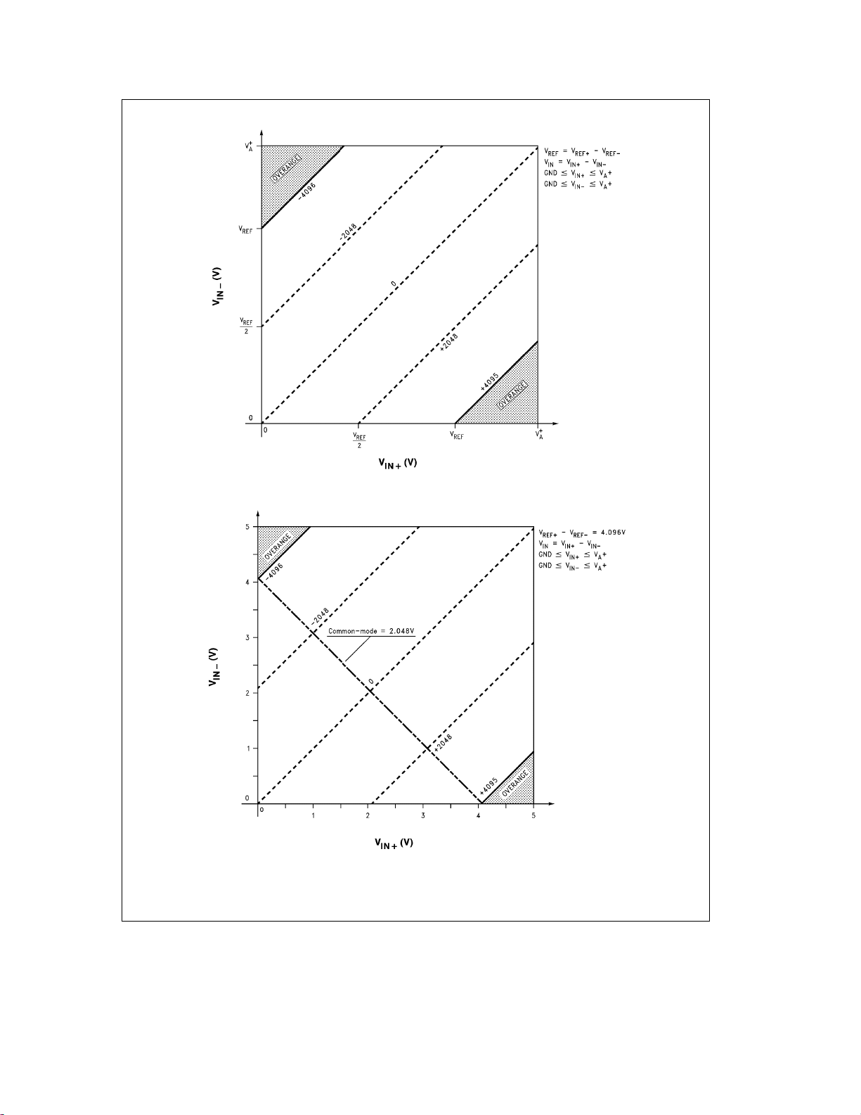
FIGURE 1. Output Digital Code vs the Operating Input Voltage Range (General Case)
FIGURE 2. Output Digital Code vs the Operating Input Voltage Range for V
REF
e
TL/H/11879– 6
TL/H/11879– 7
4.096V
15

3.0 Electrical Characteristics (Continued)
FIGURE 3. V
FIGURE 4. V
Operating Range (General Case)
REF
Operating Range for V
REF
TL/H/11879– 8
a
e
5V
A
TL/H/11879– 9
16

3.0 Electrical Characteristics (Continued)
FIGURE 5a. Transfer Characteristic
FIGURE 5b. Simplified Error Curve vs Output Code without Auto-Calibration or Auto-Zero Cycles
TL/H/11879– 10
TL/H/11879– 11
17

3.0 Electrical Characteristics (Continued)
FIGURE 5c. Simplified Error Curve vs Output Code after Auto-Calibration Cycle
TL/H/11879– 13
FIGURE 6. Offset or Zero Error Voltage
TL/H/11879– 12
18

4.0 Typical Performance Characteristics
The following curves apply for 12-bitasign mode after auto-calibration unless otherwise specified. The performance for 8-bit
sign and ‘‘watchdog’’ modes is equal to or better than shown. (Note 9)
Linearity Error Change
vs CLK Frequency
Linearity Error Change
vs Temperature
Linearity Error Change
vs Reference Voltage
a
Linearity Error Change
vs Supply Voltage
Full-Scale Error Change
vs Reference Voltage
Zero Error Change
vs Temperature
Full-Scale Error Change
vs CLK Frequency
Full-Scale Error
vs Supply Voltage
Zero Error Change
vs Reference Voltage
Full-Scale Error Change
vs Temperature
Zero Error Change
vs CLK Frequency
Zero Error Change
vs Supply Voltage
TL/H/11879– 14
19

4.0 Typical Performance Characteristics (Continued)
a
The following curves apply for 12-bit
sign and ‘‘watchdog’’ modes is equal to or better than shown. (Note 9)
sign mode after auto-calibration unless otherwise specified. The performance for 8-bit
a
Analog Supply Current
vs Temperature
The following curves apply to the LM12L438 in 12-bitasign mode after auto-calibration unless otherwise specified. R
e
T
A
100 kHz.
25§C, V
a
a
e
e
V
A
3.3V, V
D
REF
e
Unipolar Spectral Response with
10 kHz Sine Wave at 0 dB
*Digital Supply Current
vs Clock Frequency
*Free-running conversion and SPI mode data
read at 200 ns SCLK period.
2.5V, f
CLK
e
6 MHz, f
SCLK
e
8 MHz, V
Unipolar Spectral Response with
20 kHz Sine Wave at 0 dB
*Digital Supply Current
vs Temperature
e
2.5Vx0 dB, Sampling Rate
IN
TL/H/11879– 15
e
50X,
S
e
The following curves apply for 12-bitasign mode after auto-calibration unless otherwise specified. R
a
a
e
V
A
e
V
5V, V
D
e
4.096V, f
REF
CLK
Unipolar Special Response
with 41.2 kHz Sine Wave
at 0 dB Reading Data
during Conversion f
e
8 MHz, f
SCLK
SCLK
e
e
10 MHz, V
10 MHz
e
4.096Vx0 dB, Sampling Ratee100 kHz.
IN
Unipolar Special Response
with 41.2 kHz Sine Wave
at 0 dB Reading Data
between Conversions
20
TL/H/11879– 84
e
50X,T
S
TL/H/11879– 55
e
25§C,
A

4.0 Typical Performance Characteristics (Continued)
a
The following curves apply for 12-bit
e
R
S
Sampling Rate
50X,T
e
A
e
133.3 kHz.
25§C, V
a
A
Unipolar Signal-to-Noise Ratio
vs Input Frequency
sign mode after auto-calibration unless otherwise specified.
a
e
e
V
5V, V
D
e
4.096V, f
REF
Unipolar Signal-to-Noise
a
CLK
Distortion
e
8 MHz, f
vs Input Frequency
SCLK
e
10 MHz, V
Unipolar Total
Harmonic Distortion
vs Input Frequency
e
4.096Vx0 dB,
IN
Unipolar Spurious Free
Dynamic Range
vs Input Frequency
Unipolar Spectral Response
with 40.283 kHz
Sine Wave at 0 dB
Unipolar Spectral Response
with 62.256 kHz
Sine Wave at 0 dB
Unipolar Spectral Response
with 1.025 kHz
Sine Wave at 0 dB
Unipolar Spectral Response
with 40.283 kHz
Sine Wave at
Unipolar Two Tone Spectral
Response with f1
e
f2
b
0.5 dB
e
19.190 kHz and
19.482 kHz Sine Wave
Unipolar Spectral Response
with 10.010 kHz
Sine Wave at 0 dB
Unipolar Spectral Response
with 40.283 kHz
Sine Wave at
b
1.0 dB
TL/H/11879– 17
TL/H/11879– 24
21

4.0 Typical Performance Characteristics (Continued)
a
The following curves apply for 12-bit
e
R
S
Sampling Rate
50X,T
e
A
e
133.3 kHz.
25§C, V
a
A
Bipolar Signal-to-Noise Ratio
vs Input Frequency
sign mode after auto-calibration unless otherwise specified.
a
e
e
V
5V, V
D
e
4.096V, f
REF
Bipolar Signal-to-Noise
a
Distortion vs
CLK
e
8 MHz, f
Input Frequency
SCLK
e
10 MHz, V
e
g
IN
Bipolar Total Harmonic
Distortion vs Input Frequency
4.096Vx0 dB,
Bipolar Spurious Free
Dynamic Range
vs Input Frequency
Bipolar Spectral Response
with 40.283 kHz
Sine Wave at 0 dB
Bipolar Spectral Response
with 62.25 kHz
Sine Wave at 0 dB
Bipolar Spectral Response
with 1.025 kHz
Sine Wave at 0 dB
Bipolar Spectral Response
with 40.283 kHz
Sine Wave at
Bipolar Two Tone Spectral
Response with f1
e
f2
b
0.5 dB
e
19.190 kHz and
19.482 kHz Sine Waves
Bipolar Spectral Response
with 10.010 kHz
Sine Wave at 0 dB
Bipolar Spectral Response
with 40.283 kHz
Sine Wave at
b
1.0 dB
TL/H/11879– 25
TL/H/11879– 26
22

5.0 Pin Descriptions
TABLE I. LM12ÀLÓ438 Pin Description
Pin Number
PLCC SO
Pkg. Pkg.
1 7 DGND Digital ground. This is the device’s digital supply ground connection. It should be connected
2 8 IN0 These are the eight analog inputs to the multiplexer. For each conversion to be performed, the
3 9 IN1 active channels are selected according to the instruction RAM programming. Any individual
4 10 IN2 channel can be selected for a single-ended conversion referenced to AGND, or any pair of
5 11 IN3 channels, whether adjacent or non adjacent, can be selected as a fully differential input pairs.
6 12 IN4
7 13 IN5
8 14 IN6
9 15 IN7
10 16 V
11 17 V
12 18 AGND Analog ground. This is the device’s analog supply ground connection. It should be connected
13 19 V
14 20 DGND Digital ground. See above definition.
15 21 V
16 22 voltage range is
17 23 P5 P1 –P5 are the multi-function serial interface input or output pins that have different assignments
18 24 P4 Serial interface input/output: Standard: DO
19 25 P3 Serial interface input: Standard: DI
Pin Name Description
through a low resistance and low inductance ground return to the system power supply.
a
REF
Positive reference input. The operating voltage range for this input is 1VsV
Figures 3
and4). In order to achieve 12-bit performance this pin should be by passed to AGND
at least with a parallel combination of a 10 mF and a 0.1 mF (ceramic) capacitor. The capacitors
should be placed as close to the part as possible.
b
REF
Negative reference input. The operating voltage range for this input is 0 VsV
b
1V (See
Figures 3
and4). In order to achieve 12-bit performance, this pin should be bypassed
to AGND at least with a parallel combination of a 10 mF and a 0.1 mF (ceramic) capacitor. The
capacitors should be placed as close to the part as possible.
through a low resistance and low inductance ground return to the system power supply.
a
A
Analog supply. This is the supply connection for the analog circuitry. The device operating supply
voltage range is
a
3.0V toa5.5V. Accuracy is guaranteed only if the V
connected to the same potential. In order to achieve 12-bit performance, this pin should be
bypassed to AGND at least with a parallel combination of a 10 mF and a 0.1 mF (ceramic)
capacitor. The capacitors should be placed as close to the part as possible.
a
D
Digital supply. This is the supply connection for the analog circuitry. The device operating supply
a
3.0V toa5.5V. The device accuracy is guaranteed only if the V
are connected to the same potential. In order to achieve 12-bit performance this pin should be
by passed to DGND at least with a parallel combination of a 10 mF and a 0.1 mF (ceramic)
capacitor. The capacitors should be placed as close to the part as possible.
depending on the selected mode.
Serial interface input: Standard: SCLK
8051: TXD
2
I
C: SCL
TMS320: DR
8051: RXD
I2C: SDA
TMS320: DR
8051: CS
2
I
C: SAD2
TMS320: DX
a
a
s
V
REF
a
and V
A
REF
A
b
s
V
REF
a
are
D
a
and V
A
(See
a
D
a
23

5.0 Pin Descriptions (Continued)
TABLE I. LM12
Pin Number
PLCC SO
Pin Name Description
Pkg. Pkg.
20 26 P2 Serial interface input: Standard: CS
21 27 P1 Serial interface input: Standard: R/F (Clock rise/fall)
22 28 MODESEL2 Serial mode selection inputs. The logic states of these inputs determine the operation of
23 1 MODESEL1 the serial mode as shown below. The standard mode covers the National’s MICROWIRE,
Motorola’s SPI and Hitachi’s SCl protocols.
MODESEL1, MODESEL2: 01 Standard mode
24 2 CLK The device main clock input. The operating range of clock frequency is 0.05 MHz to
10.0 MHz. The device accuracy is guaranteed only for the clock frequencies indicated in
the specification tables.
25 3 INT Interrupt output. This is an active low output. An interrupt is generated any time a non-
masked interrupt condition takes place. There are seven different conditions that can
generate an interrupt. (Refer to Section 6.2.4). The interrupt is set high (inactive) by reading
the interrupt status register. This output can drive up to 100 pF of capacitive loads. An
external buffer should be used for driving higher capacitive loads.
26 4 SYNC Synchronization input/output. SYNC is an input if the Configuration Register’s SYNC I/O bit
is ‘‘0’’ and output when the bit is ‘‘1’’. When sync is an input, a rising edge on this pin
causes the internal S/H to hold the input signal and a conversion cycle or a comparison
cycle (depending on the programmed instruction) to be started. (The conversion or
comparison actually begins on the rising edge of the CLK immediately following the rising
edge of sync.) When output, it goes high at the start of a conversion or a comparison cycle
and returns low when the cycle is completed. At power up the SYNC pin is set as an input.
When used as an output it can drive up to 100 pF of capacitive loads. An external buffer
should be used for driving higher capacitive loads.
27 5 STANDBYOUT Stand-by output. This is an active low output. STANDBYOUT will be activated when the
LM12ÀLÓ438 is put into stand-by mode through the Configuration Register’s stand-by bit. It
is used to force any other devices in the system (signal conditioning circuitry, for example)
to go into power-down mode. This is done by connecting the ‘‘shutdown’’, ‘‘powerdown’’,
‘‘standby’’, etc. pins of the other ICs to STANDBYOUT
ICs do not have the power-down inputs, STANDBYOUT
through an electronic switch. Note that the logic polarity of the STANDBYOUT
opposite to that of the stand-by bit in the Configuration Register.
28 6 V
a
D
Digital supply. See above definition.
LM12434 Pin Description. (Same as LM12
LM12434 Pin Description (Same As LM12
6 12 MUXOUT
7 13 MUXOUT
8 14 S/H IN
9 15 S/H IN
b
b
a
Multiplexer outputs. These are the LM12434’s externally available analog MUX output pins.
a
Analog inputs are directed to these outputs based on the Instruction RAM programming.
Sample-and-hold inputs. These are the inverting and non-inverting inputs of the sampleand-hold. LM12434 allows external analog signal conditioning circuits to be placed
between MUX outputs and S/H inputs.
ÀLÓ
438 Pin Description (Continued)
8051: 1
2
I
C: SAD1
TMS320: FSX
8051: 1
2
I
C: SAD0
TMS320: FSR
00 8051
10 I
2
11 TMS320
ÀLÓ
438 with the exceptions of the following pins.)
ÀLÓ
438 with the exception of the following pins.)
C
. In those cases where the peripheral
can be used to turn off their power
is the
24

6.0 Operational Information
6.1 FUNCTIONAL DESCRIPTION
ÀLÓ
The LM12434 and LM12
Acquisition Systems that include a fully differential 12-bitplus-sign self-calibrating analog-to-digital converter (ADC)
with a two’s-complement output format, an 8-channel
ÀLÓ
(LM12
438) or a 4-channel (LM12434) analog multiplexer, a first-in-first-out (FIFO) register that can store 32 conversion results, and an Instruction RAM that can store as
many as eight instructions to be sequentially executed. The
LM12434 also has a differential multiplexer output and a
differential S/H input. All of this circuitry operates on only a
a
single
5V power supply. For simplicity, the DAS (Data Acquisition System) abbreviation is used as a generic name for
the members of the LM12434 and LM12
thoughout this discussion.
Figure 7
illustrates the functional block diagram or user programming model of the DAS. Note that this diagram is not
meant to reflect the actual implementation of the internal
building blocks. The model consists of the following blocks:
Ð A flexible analog multiplexer with differential output at
the front end of the device.
Ð A fully-differential, self-calibrating 12-bit
converter with sample and hold.
Ð A 32-word FIFO register as the output data buffer.
Ð An 8-word instruction RAM that can be programmed to
repeatedly perform a series of conversions and comparisons on selected input channels.
Ð A series of registers for overall control and configuration
of DAS operation and indication of internal operational
status.
Ð Interrupt generation logic to request service from the
processor under specified conditions.
Ð Serial interface logic for input/output operations be-
tween the DAS and the processor. All the registers
shown in the diagram can be read and most of them can
also be written to by the user through the input/output
block.
Ð A controller unit that manages the interactions of the
different blocks inside the DAS and controls the conversion, comparison and calibration sequences.
The DAS has 3 different modes of operation:
Ð 12-bit
a
sign conversion
Ð 8-bitasign conversion
Ð 8-bitasign comparison (also called ‘‘watchdog’’ mode)
The fully differential 12-bit-plus-sign ADC uses a charge redistribution topology that includes calibration capabilities.
Charge re-distribution ADCs use a capacitor ladder in place
of a resistor ladder to form an internal DAC. The DAC is
used by a successive approximation register to generate
intermediate voltages between the voltages applied to
b
V
and V
REF
pared against the sampled analog input voltage as each bit
a
. These intermediate voltages are com-
REF
is charged.
Conversion accuracy is ensured by an internal auto-calibration system. Two different calibration modes are available;
one compensates for offset voltage, or zero error, while the
other corrects the ADC’s linearity and offset errors.
When correcting offset only, the offset error is measured
once and a correction coefficient is created. During the full
calibration, the offset error is measured eight times, aver-
438 are multi-functional Data
ÀLÓ
438 family
a
sign ADC
aged, and a correction coefficient is created. After completion of either calibration mode, the offset correction coefficient is stored in an internal offset correction register.
The LM12434 and LM12
ÀLÓ
438’s overall linearity correction
is achieved by correcting the internal DAC’s capacitor mismatch. Each capacitor is compared eight times against all
remaining smaller value capacitors and any errors are averaged. A correction coefficient is then created and stored in
one of the thirteen linearity correction registers. A state machine, using patterns stored in 16-bit x 8-bit ROM, executes
each calibration algorithm.
Once the converter has been calibrated, an arithmetic logic
unit (ALU) uses the offset correction coefficient and the 13
linearity correction coefficients to reduce the conversion’s
offset error and linearity error, in the background, during the
a
12-bit
‘‘watchdog’’ comparisons use only the offset coefficient. An
8-bit
needed for a 12-bit
sign conversion. 8-bitasign conversions and
a
sign conversion requires less than half the time
a
sign conversion.
Diagnostic Mode
A diagnostic mode is available that allows verification of the
ÀLÓ
LM12
438’s operation. The diagnostic mode is disabled
in the LM12434. This mode internally connects the voltages
present at the V
b
and V
IN
Diagnostic bit (Bit 11) in the Configuration register to a ‘‘1’’.
a
and V
REF
S/H inputs. This mode is activated by setting the
b
pins to the internal V
REF
IN
More information concerning this mode of operation can be
found in Section 6.2.2.
Watchdog Mode
In the watchdog mode no conversion is performed, but the
DAS samples an input and compares it with the values of
the two limits stored in the Instruction RAM. If the input
voltage is above or below the limits (as defined by the user)
an interrupt can be generated to indicate a fault condition.
The LM12434 and LM
ÀLÓ
438’s ‘‘watchdog’’ mode is used
to monitor a single-ended or differential signal’s amplitude
and generate an output if the signal’s amplitude falls outsidde of a programmable ’‘window’’. Each watchdog instruction includes two limits. An interrupt can be generated if the
input signal is above or below either of the two limits. This
allows interrupt to be generated when analog voltage inputs
are ‘‘outside the window’’. After a ‘‘watchdog’’ mode interrupt, the processor can then request a conversion on the
input signal and read the signal’s magnitude.
Analog Input Multiplexer
The analog input multiplexer can be configured for any combination of single-ended or fully differential operation. Each
input is referenced to AGND when a multiplexer channel
operates in the single-ended mode. Fully differential analog
input channels are formed by pairing any two channels together.
The LM12434’s multiplexer outputs and S/H inputs
(MUXOUT
a
, MUXOUTband S/H INa, S/H INb) provide
the option for additional analog signal processing after the
multiplexer. Fixed-gain amplifiers, programmable-gain amplifiers, filters, and other processing circuits can operate on
the multiplexer output signals before they are applied to the
ADC’s S/H inputs. If external processing is not used, connect MUXOUT
a
to S/H INaand MUXOUTbto S/H INb.
a
25

6.0 Operational Information (Continued)
FIGURE 7. The LM12
(a) The LM12ÀLÓ438
ÀLÓ
438 and LM12434 Functional Block Diagram (Programming Model)
(b) The LM12434
TL/H/11879– 27
TL/H/11879– 28
26

6.0 Operational Information (Continued)
Acquisition Time
The LM12434 and LM12
to operate at its minimum acquisition time (1.125[1.5
for a 12-bit
ance, R
MHz). When 60À80ÓXkR
nal S/H’s acquisition time can be increased to a maximum
of 4.88
a
, is less than or equal to 60À80ÓX (f
S
À
6.5Óms (12asign bits, f
provide sufficient time for the sampling capacitor to charge.
See Section 6.2.1 (Instruction RAM ‘‘00’’) Bits 12–15 for
more information.
Instruction Register
The INSTRUCTION RAM is divided into 8 separate words,
each with 48 (3 x 16) bit length. Each word is separated into
three 16-bit sections. Each word has a unique address and
different sections of the instruction word are selected by the
2-bit RAM pointer (RP) in the configuration register. As
shown in
Figure 7
Instructions, Limits
tion holds operational (12-bit
dog) information such as the input channels to be selected,
the mode of operation to be performed for each instruction,
and the duration of the acquisition period. The other two
sections are used in the watchdog mode and the userdefined limits are stored in them. Each watchdog instruction
has 2 limits associated with it (usually a low limit and a high
limit, but two low limits or two high limits may be programmed instead). The DAS starts executing from instruction 0 and moves through the next instructions up to any
user-specified instruction and then ‘‘loop back’’ to instruction 0. It is not necessary to execute all 8 instructions in the
instruction loop. The cycle may be repeatedly executed until
stopped by the user. The processor should access the Instruction RAM only when the instruction sequencer is
stopped.
FIFO Register
The FIFO Register stores the conversion results. This register is ‘‘Read only’’ and all the locations are accessed
through a single address. Each time a conversion is performed the result is stored in the FIFO and the FIFO’s internal write pointer points to the next location. The pointer rolls
back to location 1 after a Write to location 32. The same
flow occurs when reading from the FIFO. The internal FIFO
Writes and the external FIFO Reads do not affect each other’s pointer locations.
ÀLÓ
438’s internal S/H is designed
sign conversion) when the source imped-
s
4.17À5.56ÓkX, the inter-
S
e8À6Ó
CLK
CLK
Ó
s
8À6
MHz) to
ms
, the Instruction RAM sections are labeled
Ý
1 and LimitsÝ2. The Instruction sec-
a
sign, 8-bitasign or watch-
Microprocessor overhead is reduced through the use of the
internal conversion FIFO. Thirty-two consecutive conversions can be completed and stored in the FIFO without any
microprocessor intervention. The microprocessor can, at
any time, interrogate the FIFO and retrieve its contents. It
Ó
can also wait for the LM12434 and LM12
interrupt when the FIFO is full or after any number (
conversions have been stored.
Configuration Register
The CONFIGURATION Register is the main ‘‘control panel’’
of the DAS. Writing 1s and 0s to the different bits of the
Configuration Register commands the DAS start or stop the
sequencer, reset the pointers and flags, go into ‘‘standby’’
mode for low power consumption, calibrate offset and linearity, and select sections of the RAM.
Other Registers
The INTERRUPT ENABLE Register lets the user activate up
to 7 sources for interrupt generation (refer to Section 6.2.3).
It also holds two user-programmable values. One is the
number of conversions to be stored in the FIFO register
before the generation of the Data Ready interrupt. The other
value is the instruction number that generates an interrupt
when the sequencer reaches that instruction.
The INTERRUPT STATUS and LIMIT STATUS Registers
are ‘‘Read only’’ registers. They are used as vectors to indicate which conditions have generated the interrupt and
what watchdog limit boundaries have been passed. Note
that the bits are set in the status registers upon occurrence
of their corresponding interrupt conditions, regardless of
whether the condition is enabled for external interrupt generation.
The TIMER Register can be programmed to insert a delay
before execution of each instruction. A bit in the instruction
register enables or disables the insertion of the delay before
the execution of an instruction.
Serial I/O
A very flexible serial synchronous interface is provided to
facilitate reading from and writing to the LM12434 and
ÀLÓ
LM12
438’s registers. The communication between the
LM12434 and LM12
ÀLÓ
438 and microcontrollers, microprocessors and other circuitry is accomplished through this
serial interface. The serial interface is designed to directly
communicate with the synchronous serial interfaces of the
most popular microprocessors with no extra hardware requirement. The interface has been also designed to simplify
software development.
ÀLÓ
438 to issue an
s
32) of
27

6.0 Operational Information (Continued)
Instruction RAM (Read/Write)
e
RP
10 RPe01 RPe00
Ý
Limits
2 LimitsÝ1 Instructions
ADDe0000 ADDe0000 ADDe0000
ADDe0001 ADDe0001 ADDe0001
ADDe0010 ADDe0010 ADDe0010
ADDe0011 ADDe0011 ADDe0011
ADDe0100 ADDe0100 ADDe0100
ADDe0101 ADDe0101 ADDe0101
ADDe0110 ADDe0110 ADDe0110
ADDe0111 ADDe0111 ADDe0111
RPeRAM Pointer
ADDeA3, A2, A1, A0 CONFIGURATION REGISTER ADDe1000
INTERRUPT ENABLE REGISTER ADDe1001
INTERRUPT STATUS REGISTER ADDe1010
TIMER REGISTER ADDe1011
CONVERSION FIFO ADDe1100
(32 Locations, 1 address) ----------------------------
LIMIT STATUS REGISTER ADDe1101
FIGURE 8. LM12434 and LM12ÀLÓ438 User Accessible Registers
----------------------------
----------------------------
(Read/Write)
(Read/Write)
(Read Only)
(Read/Write)
(Read Only)
(Read Only)
28

6.0 Operational Information (Continued)
6.2 INTERNAL USER-ACCESSIBLE REGISTERS
Figure 8
shows the LM12434 and LM12ÀLÓ438 internal user
accessible registers.
each register. All the registers are accessible through the
serial interface bus. Following are the descriptions of the
registers and their bit assignments.
6.2.1 Instruction RAM
The instruction RAM holds up to eight sequentially executable instructions. Each 48-bit long instruction is divided into
three 16-bit sections. READ and WRITE operations can be
issued to each 16-bit section using the instruction’s address
and the 2-bit ‘‘RAM pointer’’ in the Configuration register.
The eight instructions are located at addresses 0000
through 0111. They can be accessed and programmed in
random order.
Read/Write Operations
Any Instruction RAM READ or WRITE can affect the sequencer’s operation.
Therefore, the Sequencer should be stopped by setting the
RESET bit to a ‘‘1’’ or by resetting the START bit in the
Configuration Register and waiting for the current instruction
to finish execution before any Instruction RAM READ or
WRITE is initiated.
A soft RESET should be issued by writing a ‘‘1’’ to the Configuration Register’s RESET bit after any READ or WRITE to
the Instruction RAM.
The three sections in the Instruction RAM are selected by
the Configuration Register’s 2-bit ‘‘RAM Pointer’’, bits D8
and D9. The first 16-bit Instruction RAM section is selected
with the RAM Pointer equal to ‘‘00’’. This section can be
programmed for multiplexer channel selection, conversion
resolution, watchdog mode operation, timer or external
SYNC use, pause in instruction and loop bit as described
later. The second 16-bit section holds ‘‘watchdog’’ limit
its sign, and a bit that determines whether an interrupt can
be generated when the input is greater than or less than
Ý
limit
1. The third 16-bit section holds ‘‘watchdog’’ limitÝ2,
its sign, and the ‘‘greater than/less than’’ selection bit.
Instruction RAM, Bank 1, RP
Bit 0 is the LOOP bit. After an instruction with Bit 0 set to a
‘’1’’ is executed, the sequencer will loop back to instruction
0. The next instruction to be executed will be instruction 0.
Bit 1 is the PAUSE bit. When the PAUSE bit is set (‘‘1’’), the
Sequencer will stop after reading the current instruction.
The instruction will not execute at this point, and the START
bit in the Configuration register will reset to ‘‘0’’. Setting the
PAUSE also causes an interrupt to be issued. The Sequencer is restarted by placing a ‘‘1’’ in the Configuration register’s Bit 0 (Start bit).
After the Instruction RAM has been programmed and the
RESET bit is set to ‘‘1’’, the Sequencer retrieves Instruction
0, decodes it, and waits for a ‘‘1’’ to be placed in the Configuration register’s START bit. The START bit value of ‘‘1’’
‘‘overrides’’ the action of Instruction 0’s PAUSE bit when
the Sequencer is started. Once started, the Sequencer executes Instruction 0 and retrieves, decodes, and executes
Figure 9
shows the bit assignment for
e
00
Ý
each of the remaining instructions. With the PAUSE bit set
to ‘‘1’’ in instruction 0, no PAUSE Interrupt (INT 5) is generated the first time the Sequencer executes Instruction 0.
When the Sequencer encounters a LOOP bit or completes
all eight instructions, Instruction 0 is retrieved and decoded.
A set PAUSE bit in Instruction 0 now halts the Sequencer
before the instruction is executed. If Pause
tion loop continues to execute.
Bits 2 –4 select which of the eight input channels (IN0 – IN7)
will be the non-inverting inputs to the LM12
(See Table III.) They select which of the four input channels
(for IN0– IN3) will be the non-inverting inputs to the
LM12434’s ADC. (See Table IV.)
Bits 5–7 select which of the seven input channels (IN1 to
IN7) will be the inverting inputs to the LM12
(See Table III.) They select which of the three input channels (IN1 –IN4) will be the inverting inputs to the LM12434’s
ADC. (See Table IV.) Fully differential operation is created
by selecting two multiplexer channels, one non-inverting
and the other inverting. A code of ‘‘000’’ selects ground as
the inverting input for single ended operation.
Bit 8 is the SYNC bit. Setting Bit 8 to ‘‘1’’ causes the Sequencer to hold operation at the internal S/H’s acquisition
cycle and to wait until a rising edge appears at the SYNC
pin. When a rising edge appears, the S/H goes into the
‘‘Hold’’ mode and the ADC begins to perform a conversion
on the next rising edge of CLK. To make the SYNC pin
serve as an input, the Configuration register’s ‘‘SYNC I/O’’
bit (Bit 7) must be set to a ‘‘0’’. With SYNC configured as an
input, it is possible to synchronize the start of a conversion
to external events. When SYNC pin is defined as an output
(SYNC I/O bit
e
1) the SYNC bit in the instruction registers
must not be set to 1.
When the LM12434 and LM12
‘‘watchdog’’ mode with external synchronization, two rising
1,
edges on the SYNC input are required to initiate the two
ÀLÓ
438 are used in the
comparisons that are performed during a watchdog instruction. The first rising edge initiates the comparison of the
selected analog input signal with Limit
tion RAM ‘‘01’’) and the second rising edge initiates the
comparison of the same analog input signal with Limit
(found in Instruction RAM ‘‘10’’).
Bit 9 is the TIMER bit. When Bit 9 is set to ‘‘1’’, the Sequencer will halt until the internal 16-bit Timer counts down
to zero. During this time interval, no ‘‘watchdog’’ comparisons or analog-to-digital conversions will be performed.
Bit 10 selects the ADC conversion resolution. Setting Bit 10
to ‘‘1’’ selects 8-bit
a
bit
sign.
a
sign and resetting to ‘‘0’’ selects 12-
Bit 11 is the ‘‘watchdog’’ comparison mode enable bit.
When operating in the ‘‘watchdog’’ comparison mode, the
selected analog input signal is compared with the programmable values stored in Limit
Ý
1 and LimitÝ2 (see Instruction RAM ‘‘01’’ and Instruction RAM ‘‘10’’). Setting Bit 11 to
‘‘1’’ causes two comparisons of the selected analog input
signal, one with each of the two stored limits. When Bit 11 is
reset to ‘‘0’’, an 8-bit
a
sign or 12-bitasign (depending on
the state of Bit 10 of Instruction RAM ‘‘00’’) conversion of
the input signal can take place.
e
0, the instruc-
ÀLÓ
438’s ADC.
ÀLÓ
438 ADC.
Ý
1 (found in Instruc-
Ý
2
29

6.0 Operational Information (Continued)
A4 A3 A2 A1 Purpose Type D15 D14 D13 D12 D11 D10 D9 D8 D7 D6 D5 D4 D3 D2 D1 D0
0000
0111
0000
0111
0000
0111
1000
1001
1010
1011
1100
1101
*LM12434 (Refer to Table IV).
²
LM12ÀLÓ438 only. Must be set to ‘‘0’’ for the LM12434.
X No interrupt is associated with this bit. When programming the interrupt Enable Register, bit-6 is a don’t care condition.
to
to
to
Instruction RAM
(RAM Pointer
Instruction RAM
(RAM Pointer
Instruction RAM
(RAM Pointer
Configuration R/W
Register
Interrupt Enable
Register
Interrupt Status
Register
Timer R/W
Register
Conversion
FIFO
Limit Status R
Register
R/W
e
00) Time dog
R/W
e
01)
R/W
e
10)
R/W
Acquisition Watch- S/H IN
Don’t Care
Don’t Care
Don’t Care DIAG
Number of Conversion
Results in FIFO to
Generate Interrupt (INT2)
R
Number of Unread
Conversion Results
in FIFO
Timer Preset High Byte Timer Preset Low Byte
Instruction
Number or
R
Extended
Sign
Sign
LimitÝ2: Status LimitÝ1: Status
8/12 Timer Sync
l/k
Sign LimitÝ1
l/k
Sign LimitÝ2
Test RAM SYNC A/Z Each
²
e
0 Pointer I/O Cycle by CAL Zero
Instruction INT7 X INT5 INT4 INT3 INT2 INT1 INT0
Number to
Generate
Interrupt (INT1)
Instruction INST7 X INST5 INST4 INST3 INST2 INST1 INST0
Number
being
Executed
Conversion
Data: MSBs
b
(MUXINb)* (MUXINa)*
Stand- Full Auto-
I/S
Conversion Data: LSBs
S/H IN
a
Pause Loop
Reset Start
FIGURE 9. Bit Assignments for LM12434 and LM12ÀLÓ438 Internal Registers
30

6.0 Operational Information (Continued)
CONFIGURATION REGISTER (Read/Write):
D15 D14 D13 D12 D11 D10 D9 D8 D7 D6 D5 D4 D3 D2 D1 D0
Don’t Care Diag. Test RAM Sync A/Z Each I/S Stand- Full Auto Reset Start
D0: Start: 0 stops the instruction execution. 1 starts the instruction execution.
D1: Reset: When set to 1, resets Start bit; also resets all the bits in status registers and resets the instruction pointer to
zero. D1 will then automatically reset itself to zero after 2 clock pulses.
D2: Auto-Zero: When set to 1 a long (8-cycle) auto-zero calibration cycle is performed.
D3: Full Calibration: When set to 1 a full calibration cycle (linearity and auto-zero) is performed.
D4: Standby: When set to 1 the chip goes to low-power standby mode. Resetting the bit will return the chip to active
mode after a short delay.
D5: I/S: Instruction
result belongs; 1
Ý
or extended sign. 0eBits 13–15 of the conversion result hold the instruction number to which the
e
Bits 13 – 15 of the result hold the extended sign bit.
D6: A/Z each Cycle: When set to 1 a short auto-zero cycle is performed before each conversion.
D7: Sync I/O: 0eSync pin is input: 1eSync pin is output.
D9–D8: RAM Pointer: Selects the sections of the instruction RAM, 00
D10: This bit is used for production testing and must be kept zero for normal operation.
D11: Diagnostic: When set to 1, the LM12ÀLÓ438 will perform a diagnostic conversion along with a properly selected
instruction. This mode is not available on the LM12434.
D15–D12: Don’t Care.
INSTRUCTION RAM (Read/Write):
Instruction:
D15 D14 D13 D12 D11 D10 D9 D8 D7 D6 D5 D4 D3 D2 D1 D0
Acquisition Time Watchdog 8/12 Timer Sync MUXIN
D0: Loop: 0eGo to next instruction; 1eLoop back to in instructionÝ0.
D1: Pause: 0eNo pause; 1ePause; don’t do the instruction. The start bit in the Configuration register resets to 0 when
a pause encountered; a 1 written to the Start bit restarts the instruction execution.
D4–D2: MUXIN
a
: For the LM12ÀLÓ438, these bits select which input channel is connected to the ADC’s non-inverting input.
For the LM12434, they select which input channel is connected to MUXOUT
D7–D5: MUXINb: For the LM12ÀLÓ438, these bits select which input channel is connected to the ADC’s inverting input. For
the LM12434, they select which input channel is connected to MUXOUT
D8: Sync: 0eNormal operation, internal timing, SYNC is an output. 1eSYNC is an input; S/H and conversion
(comparison) timing are controlled by an external signal applied to SYNC pin.
D9: Timer: 0
e
Timer is not used for this instruction; 1eInstruction execution does not begin until timer counts down to
zero.
D10: 8/12: 0
e
12-bitasign resolution. 1e8-bitasign resolution.
D11: Watchdog: 0eConventional conversion (no watchdog comparison); 1eInstruction performs watchdog compari-
sons.
D15–D12: Acquisition Time: Determines S/H acquisition time
For 12-bit
Where D
For 12-bit
For 8-bit
Where R
a
sign: (9a2D) clock cycles. For 8-bitasign: (2a2D) clock cycles.
e
Contents of D15 –D12.
a
sign: Choose D for Dt0.45 x R
a
sign: Choose D for Dt0.36 x R
e
Input source resistance.
S
FIGURE 9. Bit Assignments for LM12434 and LM12
Pointer I/O Cycle by Cal Zero
e
Instruction, 01eLimitsÝ1, 10eLimitsÝ2.
S
S
[kX]
[kX]
b
b
.
c
[
MHz].
f
CLK
c
[
MHz].
f
CLK
ÀLÓ
438 Internal Registers (Continued)
a
.
MUXIN
a
Pause Loop
31

6.0 Operational Information (Continued)
INSTRUCTION RAM (Read/Write): (Continued)
Ý
Limits
1&2
D15 D14 D13 D12 D11 D10 D9 D8 D7 D6 D5 D4 D3 D2 D1 D0
Don’t Care
l/k
Sign Limit
D7–D0: Limit: 8-bit limit value.
e
D8: Sign: Sign of limit value, 0
D9:
l/k
: High Limit/Low limit. 0eInputs lower than limit generate interrupt, 1eInputs higher than limit generate
Positive; 1eNegative.
interrupt.
D15–D10: Don’t Care.
INTERRUPT ENABLE REGISTER (Read/Write):
D15 D14 D13 D12 D11 D10 D9 D8 D7 D6 D5 D4 D3 D2 D1 D0
Number of Conversion Instruction Number INT7 X INT5 INT4 INT3 INT2 INT1 INT0
Results in FIFO to to Generate
Generate Interrupt (INT2) Interrupt (INT1)
BitsÝ0 to 7 enable interrupt generation for the following conditions when the bit is set to 1.
D0: INT0: Generates an interrupt when a limit is passed in watchdog mode.
D1: INT1: Generates an interrupt when the sequencer has loaded the instruction number contained in bits D10, D9, and
D8 of the Interrupt Enable register.
D2: INT2: Generates an interrupt when the number of conversion results in the FIFO is equal to the programmed value
(D15–D11).
D3: INT3: Generates an interrupt when an auto-zero cycle is completed.
D4: INT4: Generates an interrupt when a full calibration cycle is completed.
D5: INT5: Generates an interrupt when a pause condition is encountered.
D6: This bit is a don’t care condition. No interrupt is associated with this bit.
D7: INT7: Generates an interrupt when the chip is returned from standby and is ready for operation.
D10–D8: Programmable instruction number used to generate an interrupt when that instruction has been reached.
D15–D11: Programmable number of conversion results in the FIFO to generate an interrupt.
TIMER REGISTER (Read/Write):
D15 D14 D13 D12 D11 D10 D9 D8 D7 D6 D5 D4 D3 D2 D1 D0
NeTimer Preset Value
The Timer delays the execution of an instruction if the Timer bit is set in that instruction.
The time delay is:
Delaye(32cN)a2[Clock Cycles
FIGURE 9. Bit Assignments for LM12434 and LM12
]
ÀLÓ
438 Internal Registers (Continued)
32

6.0 Operational Information (Continued)
FIFO REGISTER (Read only):
D15 D14 D13 D12 D11 D10 D9 D8 D7 D6 D5 D4 D3 D2 D1 D0
Instruction Number Sign Conversion Result
or Extended Sign
D11–D0: Conversion Result:
For 12-bitasign: 12-bit result value
For 8-bitasign: D11 – D4eresult value, D3 –D0e1110
D12: Sign: Conversion result sign bit, 0ePositive, 1eNegative
D15–D13: Instruction number associated with the conversion result or the extended sign bit for 2’s complement arithmetic,
INTERRUPT STATUS REGISTER (Read only):
D15 D14 D13 D12 D11 D10 D9 D8 D7 D6 D5 D4 D3 D2 D1 D0
BitsÝ0 to 7 are interrupt flags (vectors) that will be set to 1 when the following conditions occur. The bits are set to 1 whether
the interrupt is enabled or disabled in the Interrupt Enable register. The bits are reset to 0 when the register is read, or by a
device reset through the Configuration register.
D0: INST0: Is set to 1 when a limit is passed in watchdog mode.
D1: INST1: Is set to 1 when the sequencer has loaded the instruction number contained in bits D10, D9, and D8 of the
D2: INST2: Is set to 1 when number of conversion results in FIFO is equal to the programmed value (D15 –D11) in the
D3: INST3: Is set to 1 when an auto-zero cycle is completed.
D4: INST4: Is set to 1 when a full calibraton cycle is completed.
D5: INST5: Is set to 1 when a pause condition is encountered.
D6: Don’t care.
D7: INST7: Is set to 1 when the chip is returned from standby and is ready.
D10–D8: Holds the instruction number presently being executed or will be executed following a Pause or Timer delay.
D15–D11: Holds the number of conversion results that have been put in the FIFO but that have not yet been read by the user.
selected by bit D5 (Channel Mask) of the Configuration register.
Number of Unread Results Instruction Number INST7 X INST5 INST4 INST3 INST2 INST1 INST0
in FIFO Being Executed
Interrupt Enable register.
Interrupt Enable Register.
LIMIT STATUS REGISTER (Read only):
D15 D14 D13 D12 D11 D10 D9 D8 D7 D6 D5 D4 D3 D2 D1 D0
LimitÝ2: Status LimitÝ1: Status
The bits in this register are limit flags (vectors) that will be set to 1 when a limit is passed. The bits are associated to individual
instruction limits as indicated below.
D0: LimitÝ1 of InstructionÝ0 is passed.
Ý
D1: Limit
1 of InstructionÝ1 is passed.
D2: LimitÝ1 of InstructionÝ2 is passed.
D3: LimitÝ1 of InstructionÝ3 is passed.
D4: LimitÝ1 of InstructionÝ4 is passed.
D5: LimitÝ1 of InstructionÝ5 is passed.
Ý
D6: Limit
1 of InstructionÝ6 is passed.
D7: LimitÝ1 of InstructionÝ7 is passed.
D8: LimitÝ2 of InstructionÝ0 is passed.
D9: LimitÝ2 of InstructionÝ1 is passed.
Ý
D10: Limit
2 of InstructionÝ2 is passed.
D11: LimitÝ2 of InstructionÝ3 is passed.
D12: LimitÝ2 of InstructionÝ4 is passed.
D13: LimitÝ2 of InstructionÝ5 is passed.
Ý
D14: Limit
2 of InstructionÝ6 is passed.
D15: LimitÝ2 of InstructionÝ7 is passed.
ÀLÓ
FIGURE 9. Bit Assignments for LM12434 and LM12
438 Internal Registers (Continued)
33

6.0 Operational Information (Continued)
Bits 12 –15 store the user-programmable acquisition time.
The Sequencer keeps the internal S/H in the acquisition
mode for a fixed number of clock cycles (nine clock cycles,
for 12-bit
a
a
sign conversions and two clock cycles for 8-bit
sign conversions or ‘‘watchdog’’ comparisons) plus a
variable number of clock cycles equal to twice the value
stored in Bits 12 –15. Thus, the S/H’s acquisition time is (9
a
2D) clock cycles for 12-bitasign conversions and (2
2D) clock cycles for 8-bitasign conversions or ‘‘watchdog’’ comparisons, where D is the value stored in Bits 12 –
15. The minimum acquisition time compensates for the typical internal multiplexer series resistance of 2 kX, and any
additional delay created by Bits 12 –15 compensates for
source resistances greater than 60X
acquisition time is determined by the source impedance at
the multiplexer input. If the source resistance R
and the clock frequency is 8 MHz, the value stored in bits
12–15 (D) can be 0000. If R
tions determine the value that should be stored in
bits 12 – 15.
for 12-bitsasign
e
D
e
D
0.45 x RSxf
0.36 x RSxf
for 8-bitsasign and ‘‘watchdog’’
RSis in kX and f
higher integer value. If the value of 0 obtained from the
is in MHz. Round the result to the next
CLK
À
80XÓ. The necessary
l
60X, the following equa-
S
CLK
CLK
k
60X
S
expressions above is greater than 15, it is advisable to lower
the source impedance by using an analog buffer between
the signal source and the LM12
ÀLÓ
438’s multiplexer inputs.
The value of D can also be used to compensate for the
settling or response time of external processing circuits connected between the LM12434’s MUXOUT and S/H IN pins.
a
Instruction RAM, Bank 2 RP
The second Instruction RAM section is selected by placing
‘‘01’’ in Bits 8 and 9 of the Configuration register.
Bits 0 –7 hold ‘‘watchdog’’ limit
tion RAM ‘‘00’’ is set to a ‘‘1’’, the LM12434 and
ÀLÓ
LM12
438 performs a ‘‘watchdog’’ comparison of the
sampled analog input signal with the limit
followed by a comparison of the same sampled analog input
signal with the value found in limit
‘‘10’’).
Bit 8 holds limit
Ý
1’s sign.
Bit 9’s state determines the limit condition that generates a
‘‘watchdog’’ interrupt. A ‘‘1’’ causes a voltage greater than
Ý
limit
1 to generate an interrupt, while a ‘‘0’’ causes a volt-
age less than limit
Ý
Bits 10 – 15 are not used.
Instruction RAM, Bank 3, RP
The third Instruction RAM section is selected by placing
‘‘10’’ in Bits 8 and 9 of the Configuration register.
Bits 0 –7 hold ‘‘watchdog’’ limit
tion RAM ‘‘00’’ is set to a ‘‘1’’, the LM12434 and
ÀLÓ
LM12
438 performs a ‘‘watchdog’’ comparison of the
sampled analog input signal with the limit
struction RAM ‘‘01’’), followed by a comparison of the same
sampled analog input signal with the value found in limit
Bit 8 holds limitÝ2’s sign.
Bit 9’s state determines the limit condition that generates a
‘‘watchdog’’ interrupt. A ‘‘1’’ causes a voltage greater than
Ý
limit
2 to generate an interrupt, while a ‘‘0’’ causes a volt-
age less than limit
Ý
Bits 10 – 15 are not used.
TABLE III. LM12
ÀLÓ
438 Operating Mode Input Channel Selection through Input Multiplexer
Normal Operating Mode
Non-Inverting Input Input Channel to Be Inverting Input Input Channel to Be
Channel Selection Bits Connected to A/D Channel Selection Bits Connected to A/D
in Instruction Register Non-Inverting Input in Instruction Register Inverting Input
D4, D3, D2 (IN
a
) D7, D6, D5 (INb)
000 IN0 000 GND
001 IN1 001 IN1
010 IN2 010 IN2
011 IN3 011 IN3
100 IN4 100 IN4
101 IN5 101 IN5
110 IN6 110 IN6
111 IN7 111 IN7
e
01
Ý
1. When Bit 11 of Instruc-
Ý
Ý
2 (Instruction RAM
1 to generate an interrupt.
e
10
Ý
2. When Bit 11 of Instruc-
Ý
1 value first (In-
2 to generate an interrupt.
1 value first,
Ý
2.
34

6.0 Operational Information (Continued)
TABLE IV. LM12434 Input Channel Selection through Input Multiplexer
Normal Operating Mode
Non-Inverting Input Input Channel to Be Inverting Input Input Channel to Be
Channel Selection Bits Connected to MUX Channel Selection Bits Connected to MUX
in Instruction Register Non-Inverting Output in Instruction Register Inverting Output
D4, D3, D2 (MUXOUT
000 IN0 000 GND
001 IN1 001 IN1
010 IN2 010 IN2
011 IN3 011 IN3
1XX None 1XX None
TABLE V. LM12ÀLÓ438 Diagnostic Mode Input Channel Selection through Input Multiplexer
Non-Inverting Input Input Channel to Be Inverting Input Input Channel to Be
Channel Selection Bits Connected to A/D Channel Selection Bits Connected to A/D
in Instruction Register Non-Inverting Input in Instruction Register Inverting Input
D4, D3, D2 (IN
000 None 000 None
001 V
010 IN2 010 IN2
011 IN3 011 IN3
100 IN4 100 IN4
101 IN5 101 IN5
110 IN6 110 IN6
111 IN7 111 IN7
a
) D7, D6, D5 (MUXOUTb)
Diagnostic Mode
a
) D7, D6, D5 (INb)
REF
a
001 V
REF
b
35

6.0 Operational Information (Continued)
6.2.2 Configuration Register
The Configuration register is a 16-bit control register with
read/write capability. It acts as the LM12434’s and
ÀLÓ
LM12
438’s ‘‘control panel’’ holding global information
as well as start/stop, reset, self-calibration, and stand-by
commands.
Bit 0 is the START/STOP bit. Reading Bit 0 returns an indication of the Sequencer’s status. A ‘‘0’’ indicates that the
Sequencer is stopped and waiting to execute the next instruction. A ‘‘1’’ shows that the Sequencer is running. Writing a ‘‘0’’ halts the Sequencer when the current instruction
has finished execution. The next instruction to be executed
is pointed to by the instruction pointer found in the status
register. Writing a ‘‘1’’ to Bit 0 restarts the Sequencer with
the instruction currently pointed to by the instruction pointer.
(See Bits 8 –10 in the Interrupt Status register.)
Bit 1 is the DAS’ system RESET bit. Writing a ‘‘1’’ to Bit 1
stops the Sequencer (resetting the Configuration register’s
START/STOP bit), resets the Instruction pointer to ‘‘000’’
(found in the Interrupt Status register), clears the Conversion FIFO, and resets all interrupt flags. The RESET bit will
return to ‘‘0’’ after two clock cycles unless it is forced high
by writing a ‘‘1’’ into the Configuration register’s Standby bit.
A reset signal is internally generated when power is first
applied to the part. No operation should be started until the
RESET bit is ‘‘0’’.
Bit 2 is the auto-zero bit. Writing a ‘‘1’’ to this bit initiates an
auto-zero offset voltage calibration. Unlike the eight-sample
auto-zero calibration performed during the full calibration
procedure, Bit 2 initiates a ‘‘short’’ auto-zero by sampling
the offset once and creating a correction coefficient (full
calibration averages eight samples of the converter offset
voltage when creating a correction coefficient). If the Sequencer is running when Bit 2 is set to ‘‘1’’, an auto-zero
starts immediately after the conclusion of the currently running instruction. Bit 2 is reset automatically to a ‘‘0’’ and an
interrupt flag (Bit 3, in the Interrupt Status register) is set at
the end of the auto-zero (76 clock cycles). After completion
of an auto-zero calibration, the Sequencer fetches the next
instruction as pointed to by the Instruction RAM’s pointer
and resumes execution. If the Sequencer is stopped, an
auto-zero is performed immediately at the time requested.
Bit 3 is the calibration bit. Writing a ‘‘1’’ to this bit initiates a
complete calibration process that includes a ‘‘long’’ autozero offset voltage correction (this calibration averages
eight samples of the comparator offset voltage when creating a correction coefficient) followed by an ADC linearity
calibration. This complete calibration is started after the currently running instruction is completed if the Sequencer is
running when Bit 3 is set to ‘‘1’’. Bit 3 is reset automatically
to a ‘‘0’’ and an interrupt flag (Bit 4, in the Interrupt Status
register) will be generated at the end of the calibration procedure (4944 clock cycles). After completion of a full autozero and linearity calibration, the Sequencer fetches the
next instruction as pointed to by the Instruction RAM’s
pointer and resumes execution. If the Sequencer is stopped,
a full calibration is performed immediately at the time requested.
Bit 4 is the Standby bit. Writing a ‘‘1’’ to Bit 4 immediately
places the DAS in Standby mode. Normal operation returns
when Bit 4 is reset to a ‘‘0’’. The Standby command (‘‘1’’)
disconnects the external clock from the internal circuitry,
decreases the LM12434 and LM12
ÀLÓ
438’s internal
analog circuitry power supply current, and preserves all internal RAM contents. After writing a ‘‘0’’ to the Standby bit,
the DAS returns to an operating state identical to that
caused by exercising the RESET bit. A Standby completion
interrupt is issued after a power-up delay to allow the analog
circuitry to settle. The Sequencer should be restarted only
after the Standby completion interrupt is issued (see Note
22). The Instruction RAM can still be accessed through read
and write operations while the LM12434 and LM12
are in Standby Mode.
Bit 5 is the Channel Address Mask. If Bit 5 is set to a ‘‘1’’,
Bits 13 – 15 in the conversion FIFO will be equal to the sign
bit (Bit 12) of the conversion data. Resetting Bit 5 to a ‘‘0’’
causes conversion data Bits 13 through 15 to hold the instruction pointer value of the instruction to which the conversion data belongs.
Bit 6 selects a ‘‘short’’ auto-zero correction for every conversion. The Sequencer automatically inserts an auto-zero
before every conversion or ‘‘watchdog’’ comparison if Bit 6
is set to ‘‘1’’. No automatic correction will be performed if Bit
6 is reset to ‘‘0’’.
The DAS’ offset voltage, after calibration, has a typical drift
of 0.1 LSB over a temperature range of
This small drift is less than the variability of the change in
offset that can occur when using the auto-zero correction
with each conversion. This variability is the result of using
only one sample of the offset voltage to create a correction
value. This variability decreases when using the full calibration mode because eight samples of the offset voltage are
taken, averaged, and used to create a correction value.
Therefore, it is recommended that this mode not be used.
Bit 7 programs the SYNC pin (29) to operate as either an
input or an output. The SYNC pin becomes an output when
Bit 7 is a ‘‘1’’ and an input when Bit 7 is a ‘‘0’’. With SYNC
programmed as an input, the rising edge of any logic signal
applied to pin 29 will start a conversion or ‘‘watchdog’’ comparison. Programmed as an output, the logic level at pin 29
will go high at the start of a conversion or ‘‘watchdog’’ comparison and remain high until either have finished. See Instruction RAM ‘‘00’’, Bit 8.
Bits 8 and 9 form the RAM Pointer that is used to select
each of a 48-bit instruction’s three 16-bit sections during
read or write actions. A ‘‘00’’ selects Instruction RAM section one, ‘‘01’’ selects section two, and ‘‘10’’ selects section
three.
Bit 10 activates the Test mode that is used only during production testing. Always write ‘‘0’’ in this bit when programming the Instruction Register.
Bit 11 is the Diagnostic bit and is available only in the
ÀLÓ
LM12
438. It can be activated by setting it to a ‘‘1’’. The
Diagnostic mode, along with a properly chosen instruction,
allows verification that the LM12
ing correctly. When activated, the inverting and non-inverting inputs are connected as shown in Table V. As an example, an instruction with ‘‘001’’ for both IN
using the Diagnostic mode typically results in a full-scale
output.
6.2.3 Interrupts
The LM12434 and LM12
rupts, all with the same priority. Any of these interrupts will
cause a hardware interrupt to appear on the INT
ÀLÓ
438 have seven possible inter-
b
ÀLÓ
438’s ADC is perform-
a
ÀLÓ
438
40§Ctoa85§C.
and INbwhile
pin (31) if
36

6.0 Operational Information (Continued)
they are not masked (by the Interrupt Enable register). The
Interrupt Status register is then read to determine which of
the seven interrupts has been issued.
The Interrupt Status register must be cleared by reading it
after writing to the Interrupt Enable register. This removes
any spurious interrupts on the INT
Interrupt Enable register access.
Interrupt 0 is generated whenever the analog input voltage
on a selected multiplexer channel crosses a limit while the
LM12434 and LM12
dog’’ comparison mode. Two sequential comparisons are
made when the LM12434 and LM12
‘‘watchdog’’ instruction. Depending on the logic state of Bit
9 in the Instruction RAM’s second and third sections, an
interrupt will be generated either when the input signal’s
magnitude is greater than or less than the programmable
limits. (See the Instruction RAM, Bit 9 description.) The Limit
Status register will indicate which preprogrammed limit (
Ý
or
2) was crossed, and which instruction was executing
when the limit was crossed.
Interrupt 1 is generated when the Sequencer reaches the
instruction counter value specified in the Interrupt Enable
register’s bits 8 – 10. This flag appears before the instruction’s execution. Instructions continue to execute as programmed.
Interrupt 2 is activated when the Conversion FIFO holds a
number of conversions equal to the programmable value
stored in the Interrupt Enable register’s Bits 11–15. This
value ranges from 00000 to 11111, with 00001 to 11111
representing 1 to 31 conversions stored in the FIFO, and
00000 generating an interrupt after 32 conversions. See
Section 6.2.8 for more FIFO information.
The completion of the short, single-sampled auto-zero calibration generates Interrupt 3.
The completion of a full auto-zero and linearity self-calibration generates Interrupt 4.
Interrupt 5 is generated when the Sequencer encounters
an instruction that has its Pause bit (Bit 1 in Instruction RAM
‘‘00’’) set to ‘‘1’’.
Interrupt 7 is issued after a short delay (10 ms typ) while
the DAS returns from Standby mode to active operation using the Configuration register’s Bit 4. This short delay allows
the internal analog circuitry to settle sufficiently, ensuring
accurate conversion results (see Note 22).
6.2.4 Interrupt Enable Register
The Interrupt Enable register at address location 1001
has READ/WRITE capability. An individual interrupt’s ability
to produce an external interrupt at pin 31 (INT
plished by placing a ‘‘1’’ in the appropriate bit location. Any
of the internal interrupt-producing operations will set their
corresponding bits to ‘‘1’’ in the Interrupt Status register regardless of the state of the associated bit in the Interrupt
Enable register. See Section 2.3 for more information about
each of the eight internal interrupts.
Bit 0 enables an external interrupt when an internal ‘‘watchdog’’ comparison limit interrupt has taken place.
Bit 1 enables an external interrupt when the Sequencer has
reached the address stored in Bits 8 –10 of the Interrupt
Enable register.
Bit 2 enables an external interrupt when the Conversion
FIFO’s limit, stored in Bits 11 – 15 of the Interrupt Enable
register, has been reached.
ÀLÓ
438 are operating in the ‘‘watch-
pin generated during an
ÀLÓ
438 are executing a
Ý
) is accom-
Bit 3 enables an external interrupt when the single-sampled
auto-zero calibration has been completed.
Bit 4 enables an external interrupt when a full auto-zero and
linearity self-calibration has been completed.
Bit 5 enables an external interrupt when an internal Pause
interrupt has been generated.
Bit 6 don’t care condition.
Bit 7 enables an external interrupt when the LM12434 and
ÀLÓ
LM12
438 returns from standby to active mode (see
Note 22).
Bits 8–10 form the storage location of the user-programmable value against which the Sequencer’s address is compared. When the Sequencer reaches an address that is
equal to the value stored in Bits 8 – 10, an internal interrupt
is generated and appears in Bit 1 of the Interrupt Status
register. If Bit 1 of the Interrupt Enable register is set to ‘‘1’’,
an external interrupt will appear at pin 31 (INT
1
The value stored in bits 8 –10 ranges from 000 to 111, representing 1 to 8 instructions stored in the Instruction RAM.
After the Instruction RAM has been programmed and the
RESET bit is set to ‘‘1’’, the Sequencer is started by placing
a ‘‘1’’ in the Configuration register’s START bit. Setting the
INT 1 trigger value to 000 does not generate an INT 1 the
first time the Sequencer retrieves and decodes Instruction
000. The Sequencer generates INT 1 (by placing a ‘‘1’’ in
the Interrupt Status register’s Bit 1) the second time and
every subsequent time that the Sequencer encounters Instruction 000. It is important to remember that the Sequencer continues to operate even if an Instruction interrupt (INT
1) is internally or externally generated. The only mechanisms that stop the Sequencer are an instruction with the
PAUSE bit set to ‘‘1’’ (halts before instruction execution),
placing a ‘‘0’’ in the Configuration register’s START bit, or
placing a ‘‘1’’ in the Configuration register’s RESET bit.
Bits 11 –15 hold the number of conversions that must be
stored in the Conversion FIFO in order to generate an internal interrupt. This internal interrupt appears in Bit 2 of the
Interrupt Status register. If Bit 2 of the Interrupt Enable register is set to ‘‘1’’, an external interrupt will appear at pin 31
(INT).
6.2.5 Interrupt Status Register
This read-only register is located at address 1010. The corresponding flag in the Interrupt Status register goes high
(‘‘1’’) any time that an interrupt condition takes place,
whether an interrupt is enabled or disabled in the Interrupt
Enable register. Any of the active (‘‘1’’) Interrupt Status register flags are reset to ‘‘0’’ whenever this register is read or
a device reset is issued (see Bit 1 in the Configuration Register).
Bit 0 is set to ‘‘1’’ when a ‘‘watchdog’’ comparison limit
interrupt has taken place.
Bit 1 is set to ‘‘1’’ when the Sequencer has reached the
address stored in Bits 8 –10 of the Interrupt Enable register.
Bit 2 is set to ‘‘1’’ when the Conversion FIFO’s limit, stored
in Bits 11 – 15 of the Interrupt Enable register, has been
reached.
Bit 3 is set to ‘‘1’’ when the single-sampled auto-zero has
been completed.
Bit 4 is set to ‘‘1’’ when an auto-zero and full linearity selfcalibration has been completed.
Bit 5 is set to ‘‘1’’ when a Pause interrupt has been generated.
37
).

6.0 Operational Information (Continued)
Bit 6 no interrupt is associated with this bit. Don’t care con-
dition.
Bit 7 is set to ‘‘1’’ when the DAS returns from standby to
active mode (see Note 22).
Bits 8 – 10 hold the Sequencer’s current instruction number
while it is running.
Bits 11 –15 hold the current number of conversion results
stored in FIFO but have not been read by the user. After
each conversion, the result will be stored in the FIFO and
the contents of these bits incremented by one. Each single
read from FIFO decrements the contents of these bits by
one. If more than 32 conversion results being stored in FIFO
the numbers on these bits roll over from ‘‘11111’’ to
‘‘00000’’ and continue incrementing. If reads are performed
from FIFO more than the number of conversions stored in it,
the contents of these bits roll back from ‘‘00000’’ to
‘‘11111’’ and continue decrementing.
6.2.6 Limit Status Register
This read-only register is located at address 1101. This register is used in tandem with the Limit
ters in the Instruction RAM. Whenever a given instruction’s
input voltage exceeds the limit set in its corresponding Limit
Ý
register (
1orÝ2) a bit corresponding to the instruction
number is set in the Limit Status register. Any of the active
(‘‘1’’) Limit Status flags are reset to ‘‘0’’ whenever this register is read or a device reset is issued (see Bit 1 in the Configuration register). This register holds the status of limits
Ý
1 andÝ2 for each of the eight instructions.
Bits 0 –7 show the LimitÝ1 status. Each bit will be set high
(‘‘1’’) when the corresponding instruction’s input voltage exceeds the threshold stored in the instruction’s Limit
ister. When, for example, instruction 3 is a ‘‘watchdog’’ operation (Bit 11 is set high) and the input for instruction 3
meets the magnitude and/or polarity data stored in instruction 3’s Limit
Ý
1 register, Bit 3 in the Limit Status register
will be set to a ‘‘1’’.
Bits 8 – 15 show the Limit
high (‘‘1’’) when the corresponding instruction’s input voltage exceeds the threshold stored in the instruction’s Limit
Ý
2 register. When, for example, the input to instruction 6
meets the value stored in instruction 6’s Limit
Bit 14 in the Limit Status register will be set to a ‘‘1’’.
6.2.7 Timer
The LM12434 and LM12
ÀLÓ
timer that includes a 5-bit pre-scaler. It uses the clock signal
applied to pin 23 as its input. It can generate time intervals
of 0 through 2
21
clock cycles in steps of 25. This time interval can be used to delay the execution of instructions. It can
also be used to slow the conversion rate when converting
slowly changing signals. This can reduce the amount of redundant data stored in the FIFO and retrieved by the controller.
The user-defined timing value used by the Timer is stored in
the 16-bit READ/WRITE Timer register at location 1011 and
is pre-loaded automatically. Bits 0 – 7 hold the preset value’s
low byte and Bits 8 – 15 hold the high byte. The Timer is
Ý
1 and LimitÝ2 regis-
Ý
Ý
2 status. Each bit will be set
Ý
2 register,
438 have an on-board 16-bit
1 reg-
activated by the Sequencer only if the current instruction’s
Bit 9 is set (‘‘1’’). If the equivalent decimal value ‘‘N’’
(0
sNs
16
b
2
1) is written inside the 16-bit Timer register
and the Timer is enabled by setting an instruction’s bit 9 to a
‘‘1’’, the Sequencer will delay that instruction’s execution by
halting at state 3 (S3), as shown in
Figure 11,
for 32cN
2 clock cycles.
6.2.8 FIFO
The result of each conversion is stored in an internal readonly FIFO (First-In, First-Out) register. It is located at address 1100. This register has 32 16-bit wide locations. Each
location holds 13 bits of conversion data. Bits 0 –3 hold the
four LSBs in the 12 bits
a
sign mode. Bits 4–11 hold the eight MSBs and Bit 12
a
sign mode or ‘‘1110’’ in the 8 bits
holds the sign bit. Bits 13 – 15 can hold either the sign bit,
extending the register’s two’s complement data format to a
full sixteen bits or the instruction address that generated the
conversion and the resulting data. These modes are selected according to the logic state of the Configuration register’s Bit 5.
The FIFO status should be read in the Interrupt Status register (Bits 11 –15) to determine the number of conversion results that are held in the FIFO before retrieving them. This
will help prevent conversion data corruption that may take
place if the number of reads are greater than the number of
conversion results contained in the FIFO. Trying to read the
FIFO when it is empty may corrupt new data being written
into the FIFO. Writing more than 32 conversion results into
the FIFO by the ADC results in loss of the first conversion
results. Therefore, to prevent data loss, it is recommended
that the LM12434 and LM12
ÀLÓ
438’s interrupt capability be
used to inform the system controller that the FIFO is full.
Bits 0 –12 hold 12-bit
a
sign conversion data. Bits 0 –3 will
be 1110 when using 8-bit plus sign resolution.
Bits 13 – 15 hold either the instruction responsible for the
associated conversion data or the sign bit. Either mode is
selected with Bit 5 in the Configuration register.
Using the FIFO’s full depth is achieved as follows. Set the
value of the Interrupt Enable registers’s Bits 11–15 to
00000 and the Interrupt Enable register’s Bit 2 to a ‘‘1’’. This
generates an external interrupt when the 31st conversion is
stored in the FIFO. This gives the host processor a chance
to send a ‘‘0’’ to the LM12434 and LM12
ÀLÓ
438’s Start bit
(Configuration register) and halt the ADC before it completes the 32nd conversion. The Sequencer halts after the
current (32) conversion is completed. The conversion data
is then transferred to the FIFO and occupies the 32nd location. FIFO overflow is avoided if the Sequencer is halted
before the start of the 32nd conversion by placing a ‘‘0’’ in
the Start bit (Configuration register). It is important to remember that the Sequencer continues to operate even if
a FIFO interrupt (INT 2) is internally or externally generated. The only mechanisms that stop the Sequencer are an
instruction with the PAUSE bit set to ‘‘1’’ (halts before instruction execution), placing a ‘‘0’’ in the Configuration register’s START bit, or placing a ‘‘1’’ in the Configuration register’s RESET bit.
a
38

6.0 Operational Information (Continued)
6.3 INSTRUCTION SEQUENCER
The Sequencer uses a 3-bit counter (Instruction Pointer, or
IP) to retrieve the programmable conversion instructions
stored in the Instruction RAM. The counter is reset to 000
during chip reset or if the current executed instruction has
its Loop bit (Bit 1 in any Instruction RAM ‘‘00’’) set high
(‘‘1’’). It increments at the end of the currently executed
instruction and points to the next instruction. It will continue
to increment up to 111 unless an instruction’s Loop bit is
set. If this bit is set, the counter resets to ‘‘000’’ and execution begins again with the first instruction. If all instructions
have their Loop bit reset to ‘‘0’’, the Sequencer will execute
all eight instructions continuously. Therefore, it is important
to realize that if less than eight instructions are programmed, the Loop bit on the last instruction must be set.
Leaving this bit reset to ‘‘0’’ allows the Sequencer to execute ‘‘unprogrammed’’ instructions, the results of which may
be unpredictable.
The Sequencer’s Instruction Pointer value is readable at
any time and is found in the Status register at Bits 8 –10.
Figure 10
formed by the sequencer. The Sequencer can go through
eight states during instruction execution:
from the Instruction RAM ‘‘00’’. This state is one clock cycle
long.
This is the ‘‘rest’’ state whenever the Sequencer is stopped
using the reset, a Pause command, or the Start bit is reset
low (‘‘0’’). When the Start bit is set to a ‘‘1’’, this state is one
clock cycle long.
illustrates the instruction execution flow as per-
State 0: The current instruction’s first 16 bits are read
State 1: Checks the state of the Calibration and Start bits.
State 2: Perform calibration. If bit 2 or bit 6 of the Configu-
ration register is set to a ‘‘1’’, state 2 is 76 clock cycles long.
If the Configuration register’s bit 3 is set to a ‘‘1’’, state 2 is
4944 clock cycles long.
State 3: Run the internal 16-bit Timer. The number of
clock cycles for this state varies according to the value
stored in the Timer register. The number of clock cycles is
found by using the expression below
a
32T
2
where 0sTs2
16
b
1.
State 7: Sample the input signal and read LimitÝ1’s val-
ue if needed. The number of clock cycles for acquiring the
input signal in the 12-bit
a
sign mode varies according to
9a2D
where D is the user-programmable 4-bit value stored in bits
12–15 of Instruction RAM ‘‘00’’ and is limited to 0
sDs
15.
The number of clock cycles for acquiring the input signal in
a
the 8-bit
sign or ‘‘watchdog’’ mode varies according to
2a2D
State 6: Perform first watchdog comparison. This state is
5 clock cycles long.
State 4: Read Limit
State 5: Perform a conversion or second watchdog com-
parison. This state takes 44 clock cycles for a 12-bit
conversions or 21 clock cycles for a 8-bit
Ý
2. This state is 1 clock cycle long.
a
sign conver-
a
sign
sions. The ‘‘watchdog’’ comparison mode takes 5 clock cycles.
39

6.0 Operational Information (Continued)
FIGURE 10. Sequencer Logic Flow Chart (IPeInstruction Pointer)
40
TL/H/11879– 19

7.0 Digital Interface
2
In order to read from or write to the registers of the
LM12434 and LM12
nous interface is provided. Communication between the
LM12434 and LM12
ÀLÓ
438 a very flexible serial synchro-
ÀLÓ
438 and microcontrollers, microprocessors and other circuitry is accomplished through this
serial interface. The serial interface is designed to directly
communicate with synchronous serial interface of the most
popular microprocessors and I
2
C serial protocol with no additional hardware required. The interface has been also designed to accommodate easy and straightforward software
programming.
The LM12434 and LM12
ÀLÓ
438 supports four selectable
protocols as shown in Table VI. The MODESEL1 and
MODESEL2 inputs select the desired protocol. These pins
are normally hardwired for a selected protocol, but they can
also be controlled by the system in case a protocol change
within the system is required. P1–P5 are multi-function serial interface input or output pins that have different assignments depending on the selected interface mode.
The ‘‘Standard’’ interface mode uses a simple shift register
type of serial data transfer. It supports several microcontrollers’ serial synchronous protocols, including: National Semiconductor’s MICROWIRE/PLUS, Motorola’s SPl, QSPl, and
Hitachi’s synchronous SCl. Section 7.1.1 shows general
block diagrams of how the serial DAS, configured in the
Standard Interface Mode, can be connected to the HPC and
68HC11. Also, detailed assembly routines are included for
single writes, single reads and burst read operations.
The ‘‘8051’’ mode supports the synchronous serial interface
of the 8051 family of microcontrollers (8051 serial interface
Mode 0). It is also compatible with the serial interface in the
MCS-96 family of 16-bit microcontrollers. Section 7.2.1
shows a general block diagram of how the serial DAS, configured in the 8051 Interface Modes can be connected to
the 8051 family of mCs. Also, detailed assembly routines for
a single write, single read and burst read operations are
included.
The ‘‘TMS320’’ mode is designed to directly interact with
the serial interface of the TMS320C3x and TMS320C5x
families of digital signal processors. This interface is also
compatible with the similar serial interfaces on the
DSP56000 and the ADSP2100 families of DSP processors.
Section 7.3.1 shows a general block diagram of how the
serial DAS, configured in the TMS320 interface mode, can
be connected to the TMS320C3x family of DSP processors.
Also, detailed assembly routines for a single write, single
read and burst read operations are included.
ÀLÓ
Interface
Mode
TABLE VI. LM12434 and LM12
M0DESEL1 MODESEL2 P1 P2 P3 P4 P5
Standard 0 1 R/F CS DI DO SCLK
8051 0 0 1* 1* CS RXD TXD
TMS320 1 1 FSR FSX DX DR CLK
I2C 1 0 Slave AD0 Slave AD1 Slave AD2 SDA SCL
*Internally pulled-up
The ‘‘I
C’’ mode supports the Philips’ I2C bus specification
for both the standard (100 kHz maximum data rate) and the
fast (400 kHz maximum data rate) modes of operation. The
DAS behaves as a slave device on the I
2
and transmits the information under the control of a bus
master. Section 7.4.1 shows a general block diagram of
how the serial DAS, configured in the I
can be connected to an I
2
C bus using an I2C controller
(PCD8584).
All the serial interface modes allow for three basic types of
data transfer; these are single write, single read and burst
read. In a single write or read, 16 bits (2 bytes) of data is
written to or read from one of the registers inside the DAS.
In a burst read, multiple reads are performed from one register without having to repeatedly send the control and register address information for each read. The burst read can
be performed on any LM12434 and LM12
however it is primarily provided for multiple reads from the
FlFO register (one address, 32 locations), where a sequence of conversion results is stored.
7.1 STANDARD INTERFACE MODE
The standard interface mode is a simple shift register type
of serial data transfer. The serial clock synchronizes the
transfer of data to and from the LM12434 and LM12
The interface uses 4 lines: 2 data lines (DI and DO), a serial
clock line (SCLK) and a chip-select (CS) line. More than one
device can share the data and serial clock lines provided
that each device has its own chip-select line.
The LM12434 and LM12
ÀLÓ
438 standard mode is selected
when the MODESEL1 and MODESEL2 pins have the logic
state of ‘‘01’’.
for the LM12434 and LM12
Figure 12
shows a typical connection diagram
ÀLÓ
438 standard mode serial
interface. The CS, DI, DO, and SCLK lines are respectively
assigned to interface pins P2 through P5. The P1 pin is
assigned to a signal called R/F (Rise/Fall). The logic level
on this pin specifies the polarity of the serial clock:
Ð If R/F
e
1, data is shifted after falling edge and is stable
and captured at the rising edge of the SCLK.
Ð If R/F
e
0, data is shifted after rising edge and is stable
and captured at the falling edge of the SCLK.
438 Interface Modes and Pin Assignments
C bus and receives
2
C Interface mode,
ÀLÓ
438’s register,
ÀLÓ
438.
41

7.0 Digital Interface (Continued)
In both cases the data transfer is insensitive to idle state of
the SCLK. SCLK can stay at either logic level high or low
when not clocking (see
Data transfer in this mode is basically byte-oriented. This is
compatible with the serial interface of the target microcontrolIers and microprocessors. As mentioned, the LM12434
and LM12
cles: write cycle, read cycle and burst read cycle. At the
start of each data transfer cycle, ‘‘command byte’’ is written
to the serial DAS, followed by write or read data. The command byte informs the LM12434 and LM12
the communication cycle. The command byte carries the
following information:
Ð what type of data transfer (communication cycle) is start-
Ð which device register to be accessed
The command byte has the following format:
Note that the first bit may be either the MSB or the LSB of
the byte depending on the processor type, but it must be the
first bit transmitted to the LM12434 and LM12
Figure 11
cation cycles.
various combinations of R/F pin logic level and SCLK idle
state.
of conditions.
case of R/F
timing diagrams depict general relationships between the
SCLK edges, the data bits and CS
meant to show guaranteed timing. (See specification tables
for parametric switching characteristics.)
Write cycle: A write cycle begins with the falling edge of
CS
line synchronized by SCLK. The command byte has the
R/W and B bits equal to zero. Following the command byte,
16 bits of data (2 bytes) is shifted in on the same DI line.
ÀLÓ
438 have three different communication cy-
ed
shows the timing diagrams for different communi-
Figures 11e, f, g, h
e
. Then a command byte is written to the DAS on the DI
Figure 11
Figures 11a, b, c, d
Figure 11i
0 and low SCLK idle state. Note that these
)
ÀLÓ
438 about
TL/H/11879– 52
ÀLÓ
438.
show write cycles for
show read cycles for similar sets
shows a burst read cycle for the
. These diagrams are not
This data is written to the register addressed in the command byte (A3, A2, A1, A0). The data is interpreted as MSB
or LSB first based on the logic level of the 7th bit (MSB/
LSB) in the command byte. There is no activity on the DO
line during write cycles and the DAS leaves the DO line in
the high impedance state. CS
of the last bit, thus completing the write cycle.
Read cycle: A read cycle starts the same way as a write
cycle, except that the command byte’s R/W bits equal to
one. Following the command byte, the DAS outputs the
data on the DO line synchronized with the microcontroller’s
SCLK. The data is read from the register addressed in the
command byte. Data is shifted out MSB or LSB first, depending on the logic level of the MSB/LSB bit. The logic
state of the Dl line is ‘‘don’t care’’ after the command byte.
CS
will go high after the transfer of the last data bit, then
completing the read cycle.
Burst read cycle: A burst read cycle starts the same way
as a single read cycle, but the B bit in the command byte is
set to one, indicating a burst read cycle. Following the command byte the data is output on the DO line as long as the
DAS receives SCLK from the system. To tell the DAS when
a burst read cycle is completed pull CS
and before the 15th SCLK cycle during the last data byte
transfer (see
last data bit is transferred, the DAS is ready for a new communication cycle to begin.
The timing diagrams in
in packets of 8 bits (bytes). This represents the way the
serial ports of most microcontrollers and microprocessors
produce serial clock and data. The DAS does not require a
gap between the first and second byte of the data; 16 continuous clock cycles will transfer the data word. However,
there should be a gap equal to 3 CLK (the DAS main clock
input, not the SCLK) cycles between the end of the command byte and the start of the data during a read cycle. This
is not a concern in most systems for two reasons. First, the
processor generally has some inherent gap between byte
transfers. Second, the SCLK frequency is usually significantly slower than the CLK frequency. For example, a
68HC11 processor with an 8 MHz crystal generates a maximum SCLK frequency of 1 MHz. If the DAS is running with a
6 MHz CLK, there are 6 cycles of CLK within each cycle of
SCLK and the requirement is satisfied even if SCLK operates continuously during and after the command byte.
Figure 11i
will go high after the transfer
high after the 8th
). After CS high is detected and the
Figure 11
show the transfer of data
42

7.0 Digital Interface (Continued)
Idle State of SCLK
Idle State of SCLK
e
e
(a) Write Cycle, R/F Input (P1)e1
0, Data Stable at Rising Edge and Shifted at Falling Edge of the SCLK
(b) Write Cycle, R/F Input (P1)e1
1, Data Stable at Rising Edge and Shifted at Falling Edge of the SCLK
FIGURE 11. Timing Diagrams for LM12434 and LM12
ÀLÓ
438 Standard Serial Interface
TL/H/11879– 30
TL/H/11879– 31
43

7.0 Digital Interface (Continued)
(c) Write Cycle, R/F Input (P1)e0
Idle State of SCLK
Idle State of SCLK
e
0, Data Stable at Falling Edge and Shifted at Rising Edge of the SCLK
(d) Write Cycle, R/F Input (P1)e0
e
1, Data Stable at Falling Edge and Shifted at Rising Edge of the SCLK
FIGURE 11. Timing Diagrams for LM12434 and LM12
ÀLÓ
438 Standard Serial Interface (Continued)
TL/H/11879– 32
TL/H/11879– 33
44

7.0 Digital Interface (Continued)
Idle State of SCLK
Idle State of SCLK
e
e
(e) Read Cycle, R/F Input (P1)e1
0, Data Stable at Rising Edge and Shifted at Falling Edge of the SCLK
(f) Read Cycle, R/F Input (P1)e1
1, Data Stable at Rising Edge and Shifted at Falling Edge of the SCLK
FIGURE 11. Timing Diagrams for LM12434 and LM12
ÀLÓ
438 Standard Serial Interface (Continued)
TL/H/11879– 34
TL/H/11879– 35
45

7.0 Digital Interface (Continued)
(g) Read Cycle, R/F Input (P1)e0
Idle State of SCLK
Idle State of SCLK
e
0, Data Stable at Falling Edge and Shifted at Rising Edge of the SCLK
(h) Read Cycle, R/F Input (P1)e0
e
1, Data Stable at Falling Edge and Shifted at Rising Edge of the SCLK
FIGURE 11. Timing Diagrams for LM12434 and LM12
ÀLÓ
438 Standard Serial Interface (Continued)
TL/H/11879– 36
TL/H/11879– 37
46

7.0 Digital Interface (Continued)
TL/H/11879– 38
1
e
438 Standard Serial Interface (Continued)
Ó
L
À
(i) Burst Read Cycle, R/F Input (P1)
0, Data Stable at Rising Edge and Shifted at Falling Edge of the SCLK
e
Idle State of SCLK
FIGURE 11. Timing Diagrams for LM12434 and LM12
47

7.0 Digital Interface (Continued)
7.1.1 Examples of Interfacing to the HPC’s MICROWIRE/PLUS and 68HC11’s SPI
Note: Other device pins are not shown.
FIGURE 12a. LM12434 and LM12ÀLÓ438 Standard Mode Interface to the HPC’s MICROWIRE/PLUS
Note: Other device pins are not shown.
FIGURE 12b. LM12434 and LM12ÀLÓ438 Standard Mode Interface to the 68HC11’s SPI
TL/H/11879– 65
TM
TL/H/11879– 66
48

7.0 Digital Interface (Continued)
HPC Assembly Code Example
TL/H/11879– 56
49

7.0 Digital Interface (Continued)
HPC Assembly Code Example (Continued)
TL/H/11879– 57
50

7.0 Digital Interface (Continued)
HPC Assembly Code Example (Continued)
TL/H/11879– 58
51

7.0 Digital Interface (Continued)
HPC Assembly Code Example (Continued)
TL/H/11879– 59
68HC11 Assembly Code Example
TL/H/11879– 85
52

7.0 Digital Interface (Continued)
68HC11 Assembly Code Example (Continued)
TL/H/11879– 86
53

7.0 Digital Interface (Continued)
68HC11 Assembly Code Example (Continued)
TL/H/11879– 87
54

7.0 Digital Interface (Continued)
7.2 8051 INTERFACE MODE
The 8051 interface mode is designed to work directly with
the 8051 family of microcontrollers’ mode 0 serial interface.
This interface mode is a simple shift register type of serial
data transfer. The serial clock synchronizes the transfer of
data to and from the LM12434 and LM12
face uses 3 lines: a bidirectional data line (RXD), a serial
clock line (TXD) and a chip-select (CS
device can share the data and serial clock lines provided
that each device has its own chip-select line.
The 8051 mode is selected when the MODESEL1 and
MODESEL2 pins have the logic state of ‘‘00’’.
shows a typical connection diagram for the 8051 mode serial interface. The CS
assigned to interface pins P3 through P5. The P1 and P2
pins are not used in this mode and should be left open or
connected to logic ‘‘1’’. In this interface the idle state of the
serial clock TXD is logic ‘‘1’’. The data is stable at both
edges of the TXD clock and is shifted after its rising edge.
The interface has a bidirectional RXD data line. The
LM12434 and LM12
impedance state whenever it is not outputting any data.
Data transfer in this mode is byte oriented. As mentioned,
the LM12434 and LM12
nication cycles: write cycle, read cycle and burst read cycle.
At the start of each data transfer cycle, ‘‘command byte’’ is
written to the LM12434 and LM12
or read data. The command byte informs the LM12434 and
ÀLÓ
LM12
438 about the communication cycle and carries
the following information:
Ð what type of data transfer (communication cycle) is start-
ed
Ð which device register is to be accessed
, RXD and TXD lines are respectively
ÀLÓ
438 leaves the RXD line in a high
ÀLÓ
438 has three different commu-
ÀLÓ
438. The inter-
) line. More than one
Figure 14
ÀLÓ
438, followed by write
The command byte has the following format:
TL/H/11879– 53
The first bit is the LSB of the byte based on the 8051 mode
0 serial interface protocol.
Figure 13
cation cycles.
shows a read cycle.
Note that these timing diagrams depict general relationships
between the SCLK edges, the data bits and CS
grams are not meant to show guaranteed timing performance. (See specification tables for parametric switching
characteristics.)
Write cycle: A write cycle begins with the falling edge of the
CS
line synchronized by TXD clock. The command byte has the
R/W and B bits equal to zero. Following the command byte,
16 bits of data (2 bytes) is shifted in on the RXD line. The
data is written to the register addressed in the command
byte (A3, A2, A1, A0). The data is always LSB first in this
interface. CS
thus completing the write cycle.
Read cycle: A read cycle starts the same way as a write
cycle, except that the command bytes R/W
one. Following the command byte, the DAS outputs the
data on the RXD line synchronized with the microcontroller’s TXD clock. The data is read from the register addressed in the command byte. Data is shifted in LSB first.
Again, CS
thus completing the read cycle.
shows the timing diagrams for different communi-
Figure 13a
. Then a command byte is written to the DAS on the RXD
will go high after the transfer of the last bit,
will go high after the transfer of the last data bit,
shows a write cycle.
Figure 13c
shows a burst read cycle.
Figure 13b
. These dia-
bit is equal to
55

7.0 Digital Interface (Continued)
Burst read cycle: A burst read cycle starts the same way
as a single read cycle, but the B bit in the command byte is
set to one, indicating a burst read cycle. Following the command byte the data is output on the RXD line as long as the
DAS receives TXD clock from the system. To tell the DAS
when a burst read cycle is completed, CS
after the 8th and before the 15th SCLK cycle during the last
data byte transfer (see
Figure 13c
ed and the last data bit is transferred, the DAS is ready for a
new communication cycle to begin.
The timing diagrams in
Figure 13
in packets of 8 bits (bytes). This represents the way the
serial ports of the 8051 family of microcontrollers produce
the serial clock and data. The DAS does not require a gap
between the first and second bytes of the data;
should be set high
). After CS high is detect-
show the transfer of data
16 continuous clock cycles will transfer the data word. However, there should be a gap equal to 3 CLK (the DAS main
clock input, not the TXD clock) cycles between the end of
the command byte and the start of the data during a read
cycle. This is not concerned in most systems for two reasons. First, the processor generally has some inherent gap
between byte transfers. Second, the TXD frequency is usually significantly slower than the CLK frequency. For example, an 8051 processor with 12 MHz crystal generates a
TXD of 1 MHz. If the DAS is running with 6 MHz CLK, there
are 6 cycles of CLK within each cycle of TXD and the requirement is satisfied even if TXD comes continuously after
command byte. The user should pay attention to this requirement if running the TXD with a speed near or higher
than CLK.
(a) Write Cycle
Idle State of SCLK
Idle State of SCLK
e
1, Data Shifted at the Rising Edge of the SCLK
(b) Read Cycle
e
1, Data Shifted at the Rising Edge of the SCLK
FIGURE 13. Timing Diagrams for LM12434 and LM12
ÀLÓ
438 8051 Serial Interface Mode
TL/H/11879– 40
TL/H/11879– 41
56

7.0 Digital Interface (Continued)
TL/H/11879– 42
438 8051 Serial Interface Mode (Continued)
Ó
L
À
(c) Burst Read Cycle
1, Data Shifted after the Rising Edge of the SCLK
e
Idle State of SCLK
FIGURE 13. Timing Diagrams for LM12434 and LM12
57

7.0 Digital Interface (Continued)
7.2.1 Example of Interfacing to the 8051
FIGURE 14. LM12434 and LM12ÀLÓ438 in the 8051 Interface Mode
TL/H/11879– 67
8051 Assembly Code Example
TL/H/11879– 89
58

7.0 Digital Interface (Continued)
8051 Assembly Code Example (Continued)
TL/H/11879– 90
59

7.0 Digital Interface (Continued)
8051 Assembly Code Example (Continued)
TL/H/11879– 91
60

7.0 Digital Interface (Continued)
8051 Assembly Code Example (Continued)
TL/H/11879– 96
61

7.0 Digital Interface (Continued)
7.3 TMS320 INTERFACE MODE
The TMS320 interface mode is designed to work directly
with the serial interface port of the TMS320C3x and
TMS320C5x families of digital signal processors. This interface uses five lines: two data lines (DX, DR), two frame
synchronization signal lines (FSX, FSR), and a serial clock
line (SCLK). Note that the TMS320C3x/5x serial interface
has two separate serial clock lines for transmit and receive
called CLKX and CLKR, but the LM12434 and LM12
only uses one clock input for both receive and transmit.
Typically, CLKX is specified as an output and drives SCLK
as well as CLKR (defined as an input). The serial clock for
this interface mode is a free running clock, with the data
stream synchronized by SCLK. The start of each data transfer (the beginning of a data packet) is synchronized by FSX
(Transmit Frame Sync) or FSR (Receive Frame Sync). This
interface can communicate with one device; no device select signal is used. The following discussion assumes that
the reader has a basic knowledge of the architecture and
operation of the TMS320C3x/5x serial interface port.
The TMS320 interface mode is selected when the
MODESEL1 and MODESEL2 pins have the logic state of
‘‘11’’.
Figure 16
LM12434 and LM12
mode. The FSR, FSX, DX, DR, and SCLK lines are assigned
to interface pins P1 through P5.
Data transfer in this mode is programmable by the processor for 8-, 16-, 24-, or 32-bit data packets for the
TMS320C3x and 8-, or 16-bit data packets for TMS320C5x.
The LM12434 and LM12
packets. For the TMS320C5x the 32-bit packet is composed
of two successive 16-bit packets with no gaps between
them. The data bits in each packet are transferred MSB
first, and are shifted in on the rising edge of SCLK and are
stable and captured at the falling edge of the SCLK. As with
the ‘‘Standard’’ and ‘‘8051’’ interface modes, the LM12434
and LM12
write cycle, read cycle and burst read cycle. At the start of
each data transfer cycle, a stream of 9 data bits (the ‘‘command packet’’) is written to the LM12434 and LM12
and informs it about the communication cycle. The placement of these 9 bits in the data packet is different in the
read and write cycles and is discussed for each case separately. The command packet carries the following information:
Ð what type of data transfer (communication cycle) is start-
ed
Ð which device register is to be accessed
shows a typical connection diagram for the
ÀLÓ
438 in the TMS320 serial interface
ÀLÓ
438 uses 16-bit and 32-bit data
ÀLÓ
438 has three different communication cycles:
ÀLÓ
ÀLÓ
438
438
The command packet has the following format:
TL/H/11879– 54
The first bit of the command packet is always the MSB of
the data packet to to be transferred.
Figure 15
cation cycles.
shows a read cycle, and
cycle. Note that these timing diagrams depict general relationships between the SCLK edges, the data bits and the
frame synchronization signals (FSX, FSR). These diagrams
are not meant to show guaranteed timing performance.
(See specification tables for parametric switching characteristics.)
Write cycle: A write cycle begins with an FSX pulse from
the processor. The first data bit is received by the DAS on
the DX line during the next SCLK falling edge after the falling edge of FSX. A 32-bit data packet is written to the DAS.
The TMS320C3x does this with a 32-bit transfer, using its
serial port 32-bit register. With the TMS320C5x family two
successive 16-bit transfers are initiated without any gap in
between. The first 9 bits (MSBs) of the data are the command packet with the R/W
lowing the command packet, a 16-bit data stream starts on
the falling edge of the 10th SCLK cycle and continues
through the 25th cycle. The last 7 bits in the 32-bit data
packet are ‘‘don’t care’’ and are ignored by the DAS. The
data is written to the register addressed in the command
packet (A3, A2, A1, A0). There is no activity on the FSR and
DR lines during a write cycle. The write cycle is completed
after the last data bit is transferred.
Read cycle: A read cycle also begins with an FSX pulse
from the processor. The read cycle uses 16-bit data transfer. Following the FSX pulse, 16 bits of data are written to
the DAS on the DX line. The first 9 bits (MSBs) of data are
the command packet with the R/W
B bit equal to zero. The last 7 bits (LSBs) are ‘‘don’t care’’
and are ignored by the DAS. About 3 to 4 CLK (the DAS
main clock input, not the SCLK) cycles after the R/W
received, the DAS generates an FSR pulse to initiate the
data transfer. Following the FSR pulse, the DAS will send
16 bits of data to the processor on the DR line. The first bit
(MSB) of the data appears on the DR line on the next SCLK
cycle following the FSR pulse. The data is read from the
register addressed in the command packet. The read cycle
is completed after the last data bit is transferred.
shows the timing diagrams for the three communi-
Figure 15a
shows a write cycle.
Figure 15c
bit and B bit equal to zero. Fol-
bit equal to one and the
Figure 15b
shows a burst read
bit is
62

7.0 Digital Interface (Continued)
Burst read cycle: A burst read cycle starts the same way
as a single read cycle, but the B bit in the command packet
is set to one, indicating a burst read cycle. After the first 16
bits of data carrying the command packet is written to the
DAS, the DAS begins to send out the data words from the
addressed register on the DR line repeatedly. Each data
word is preceded by an FSR pulse for synchronization. To
terminate a burst read cycle, the processor does a dummy
read from the configuration register during the last
data word. This dummy read should be started so that its
FSR pulse occurs during the 15th to 17th SCLK cycle of the
last data word as shown in
terminates the burst read cycle and shifts out the contents
of the configuration register on the DR line. This data can be
discarded. After transfer of the last data bit from the configuration register, the DAS is ready for a new communication
cycle to begin.
Figure 15c
. The dummy read
(a) Write Cycle
(b) Read Cycle
FIGURE 15. Timing Diagram for LM12434 and LM12ÀLÓ438 TMS320 Serial Interface Mode
TL/H/11879– 47
TL/H/11879– 48
63

7.0 Digital Interface (Continued)
TL/H/11879– 49
438 TMS320 Serial Interface Mode (Continued)
Ó
L
À
(c) Burst Read Cycle
FIGURE 15. Timing Diagram for LM12434 and LM12
64

7.0 Digital Interface (Continued)
7.3.1 Example of Interfacing to the TMS320C3x
Note: Other device pins are not shown.
FIGURE 16. LM12434 and LM12ÀLÓ438 in the TMS320 Interface Mode
TL/H/11879– 75
TMS320C3x Assembly Code Example
TL/H/11879– 92
65

7.0 Digital Interface (Continued)
TMS320C3x Assembly Code Example (Continued)
TL/H/11879– 93
66

7.0 Digital Interface (Continued)
TMS320C3x Assembly Code Example (Continued)
TL/H/11879– 94
67

7.0 Digital Interface (Continued)
TMS320C3x Assembly Code Example (Continued)
TL/H/11879– 95
68

7.0 Digital Interface (Continued)
TMS320C3x Assembly Code Example (Continued)
TL/H/11879– 97
69

7.0 Digital Interface (Continued)
2
7.4 I
C BUS INTERFACE
The I2C bus is a serial synchronous bus structure. It is a
multi-master bus, which means that more than one device
capable of controlling the bus can be connected to it. The
bus uses 2 wires, serial data (SDA) and serial clock (SCL),
to carry information between the devices connected to the
bus. Both data and clock lines are bidirectional and are connected to the positive power supply via a pull-up resistor.
Each device is identified by a unique address, whether it is a
microprocessor/controller or a peripheral such as memory,
keyboard, data-converter or display. Each device can operate as either transmitter or receiver, depending on the function of the device. In addition to transmitters and receivers,
devices can also be considered as masters and slaves
when performing data transfer. A master is the device that
initiates a data transfer on the bus and generates the clock
signals to permit that transfer. At that time, any device addressed is considered slave. It should be apparent that the
2
I
C bus is not merely an interconnecting wire, it embodies
comprehensive formats and procedures for addressing,
transfer cycles start and stop, clock generation/synchronization and bus arbitration. The following discussion assumes that the reader is familiar with the specification and
architecture of the I
The LM12434 and LM12ÀLÓ438’s I2C bus interface is selected when the MODESEL1 and MODESEL2 pins have the
logic state of ‘‘10’’.
diagram for the LM12434 and LM12
As was mentioned, communication on the I
formed on 2 lines, SCL (serial clock) and SDA (serial data);
pins P5 and P4 are assigned to these lines. The DAS operates as a slave on the I
an input (no clock is generated by the LM12434 and
ÀLÓ
LM12
438) and the SDA line is a bi-directional serial data
path. According to I
7-bit slave address. The four most significant bits of the
slave address are hard wired inside the LM12434 and
ÀLÓ
LM12
438 and are ‘‘0101’’. The three least significant
bits of the address are assigned to pins P3–P1. Therefore,
the LM12434 and LM12
MSB LSB
Tying the P3 –P1 pins to different logic levels allows up to
eight LM12434 and LM12
2
single I
C bus.
Figure 17
cycles for the LM12434 and LM12
2
C bus.
Figure 18
2
C bus specifications, the DAS has a
shows a typical connection
ÀLÓ
438 to the I2C bus.
2
C bus is per-
2
C bus. As a result, the SCL line is
ÀLÓ
438 I2C slave address is:
0 1 0 1 P3 P2 P1
ÀLÓ
438’s to be addressed on a
shows the timing diagram for the read and write
ÀLÓ
438’s I2C interface.
This timing diagram depicts the general relationship between the serial clock edges and the data bits. It is not
meant to show guaranteed timing performance. (See specification tables for parametric switching characteristics.) The
2
DAS’s I
C interface timing parameters fully meet or exceed
2
the I
C bus specification. Data transfer on the I2C bus is
byte oriented and the 16-bit data to be written to or read
from each register is transferred in two bytes.
Write cycle: A write cycle is illustrated in
munication is initiated with a start condition generated by a
2
master (I
C bus specification), followed by a byte of the
Figure 17a
. Com-
DAS’s slave address with the read/write bit (8th bit) being
‘‘0’’, indicating a write cycle will follow. At the 9th SCL clock
pulse of the first data packet, the DAS pulls the SDA line
low (‘‘0’’) to acknowledge that it has been addressed. The
next byte is the address of the DAS register to be accessed.
The format of this byte is three ‘‘0’s’’ (MSBs) followed by
four bits of register address (MSB first as shown) and a ‘‘0’’
as the last bit (LSB). After the DAS acknowledges the address byte, the 16-bit data proceeds in two bytes, beginning
with the high order byte (MSB first). The direction of the
data in a write cycle is from master to DAS with acknowledgement given by the DAS at the end of each byte. The
cycle is completed by a stop condition generated by the
master.
Read/burst read cycle: The read and burst read cycles for
2
the I
C interface are combined in a single format. A read
cycle is shown in
Figure 17b
. A read cycle starts the same
as a write with a slave address byte for write followed by a
register address byte. After the register address byte is written to the DAS, the bus should be released without any stop
condition. The master then applies a repeat start condition
followed by the DAS’s slave address, but with the read/
write bit being ‘‘1’’, indicating a read request from the master. The DAS (slave) acknowledges its address and beginning with the next byte, the direction of the data will be from
DAS to master. The DAS starts to transmit the contents of
its register (addressed previously at second byte of the cycle) synchronized with the clocks applied by the master. An
even number of data bytes should be read from the DAS
(two bytes per register). At the end of each byte received
from the DAS the bus master generates an acknowledge.
The DAS continues to repeat transmitting its register contents as long as the master is transmitting clocks and acknowledges at the end of each byte. The DAS recognizes
the end of the transfer whenever the master does not acknowledge at the end of an even numbered byte. At this
point, the master should generate a stop condition as required by the I
2
C bus specification. Notice that the master
may read only one word (single read) or as many words (two
bytes each) as it needs using the read procedure.
70

7.0 Digital Interface (Continued)
TL/H/11879– 44
TL/H/11879– 45
C Interface
2
438 I
Ó
L
À
(a) Write Cycle
(b) Read Cycle/Burst Read Cycle
FIGURE 17. Timing Diagrams for LM12434 and LM12
*n should be an even number.
71

7.0 Digital Interface (Continued)
7.4.1 Example of Interfacing to an I
2
C Bus Controller (No Assembly Code)
Note: Other device pins are not shown.
TL/H/11879– 82
FIGURE 18. Interfacing the DAS to an I2C Bus Controller
72

8.0 Analog Considerations
8.1 REFERENCE VOLTAGE
The difference between the voltages applied to the V
and V
between the voltages applied across two multiplexer inputs
is the analog input voltage span (the difference
b
REF
or the voltage applied to one of the multiplexer inputs and
analog ground, over which 4095 positive and 4096 negative
codes exist). The voltage sources driving V
must have very low output impedance and noise. The circuit
in
Figure 19
is an example of a very stable reference appro-
priate for use with the LM12434 and LM12
REF
ÀLÓ
The ADC can be used in either ratiometric or absolute reference applications. In ratiometric systems, the analog input
voltage is proportional to the voltage used for the ADC’s
reference voltage. When this voltage is the system power
supply, the V
connected to GND. This technique relaxes the system refer-
pin is connected to V
a
REF
a
A
ence stability requirements because the analog input voltage and the ADC reference voltage move together. This
maintains the same output code for given input conditions.
For absolute accuracy, where the analog input voltage varies between very specific voltage limits, a time and temperature stable voltage source can be connected to the reference inputs. Typically, the reference voltage’s magnitude
will require an initial adjustment to null reference voltage
induced full-scale errors.
8.2 INPUT RANGE
The LM12434 and LM12
ÀLÓ
438’s fully differential ADC and
reference voltage inputs generate a two’s-complement output that is found by using the equation below.
b
V
V
a
IN
output code
output code
e
V
REF
V
IN
e
V
REF
Round up to the next integer value between
for 12-bit resolution and between
olution if the result of the above equation is not a whole
number. As an example, V
e
V
1.5V and V
a
IN
code is positive full-scale, or 0,1111,1111,1111. If V
e
5V, V
REF
a
12-bit
sign output code is 0,1100,0000,0000.
IN
e
1V, V
b
b
IN
b
a
b
a
b
a
e
b
a
IN
(4096)b(/2 (12-bit)
V
b
REF
V
b
IN
(256)b(/2 (8-bit)
V
b
REF
b
a
REF
GND. The 12-bitasign output
e
3V, and V
b
256 to 255 for 8-bit res-
e
2.5V, V
b
IN
REF
or V
a
REF
438.
and V
REF
b
4096 to 4095
e
b
REF
REF
e
GND, the
1V,
8.3 INPUT CURRENT
A charging current flows into or out of (depending on the
a
input voltage polarity) the analog input pins, IN0 – IN7 at the
start of the analog input acquisition time (t
rent’s peak value will depend on the actual input voltage
applied.
b
8.4 INPUT SOURCE RESISTANCE
For low impedance voltage sources (
k
ation), the input charging current will decay, before the end
of the S/H’s acquisition time, to a value that will not introduce any conversion errors. For higher source impedances,
the S/H’s acquisition time can be increased. As an example, operating with a 8 MHz clock frequency and maximum
acquisition time, the LM12434 and LM12438’s analog inputs
is
can handle source impedances as high as 4.17 kX. Refer to
Section 6.2.1, Instruction RAM ‘‘00’’, Bits 12 –15 for further
information.
8.5 INPUT BYPASS CAPACITANCE
External capacitors (0.01 mF – 0.1 mF) can be connected between the analog input pins, IN0 – IN7, and analog ground to
filter any noise caused by inductive pickup associated with
long input leads. These capacitors will not degrade the conversion accuracy.
8.6 INPUT NOISE
The leads to each of the analog multiplexer input pins
should be kept as short as possible. This will minimize input
noise and clock frequency coupling that can cause conversion errors. Input filtering can be used to reduce the effects
of the noise sources.
8.7 POWER SUPPLY CONSIDERATIONS
Decoupling and bypassing the power supply on a high resolution ADC is an important design task. Noise spikes on the
a
V
(analog supply) or V
A
conversion errors. The analog comparator used in the ADC
a
(digital supply) can cause
D
will respond to power supply noise and will make erroneous
conversion decisions. The DAS is especially sensitive to
power supply spikes that occur during the auto-zero or linearity calibration cycles.
a
). This cur-
ACQ
60X for 8 MHz oper-
FIGURE 19. Low Drift Extremely Stable Reference Circuit
73
*Tantalum
**Ceramic
TL/H/11879– 20

8.0 Analog Considerations (Continued)
a
a
D
) and 1
a
D
Figure
5V
The LM12434/8 is designed to operate from a single
power supply. The LM12
a
a single
3.3V supply. The separate supply and ground
ÀLÓ
438 is designed to operate from
pins for the analog and digital portions of the circuit allow
separate external bypassing. To minimize power supply
noise and ripple adequate bypass capacitors should be
placed directly between power supply pins and their associated grounds. Both supply pins are generally connected to
the same supply source. In systems with separate analog
and digital supplies, the DAS should be powered from the
analog supply. At least a 10 mF tantalum electrolytic capacitor in parallel with a 0.1 mF monolithic ceramic capacitor is
recommended for bypassing each power supply. The key
consideration for these capacitors is to have the low series
resistance and inductance. The capacitors should be placed
as close as physically possible to the supply and ground
pins with the smaller capacitor closer to the device. The
capacitors also should have the shortest possible leads in
order to minimize series lead inductance. Surface mount
chip capacitors are optimal in this respect and should be
used when possible.
When the power supply regulator is not local on the board,
adequate bypassing (a high value electrolytic capacitor)
should be placed at the power entry point. The value of the
capacitor depends on the total supply current of the circuits
on the PC board. All supply currents should be supplied by
the capacitor instead of being drawn from the external supply lines, while the external supply charges the capacitor at
a steady rate.
The DAS has two V
package. It is recommended to use a 0.1 mFplusa10mF
capacitor between pins 15 and 16 (V
and a 0.1 mF capacitor between pins 28 (V
(DGND) for the PLCC package. The respective pins for the
SO package are 21 and 22 (V
and 7 (DGND). The layout diagrams in Section 8.8 show the
a
and DGND pins on two sides of its
D
a
) and 14 (DGND)
D
a
) and 20 (DGND), 6 (V
D
recommended placement for the supply bypass capacitors.
8.8 PC BOARD LAYOUT AND GROUNDING
CONSIDERATIONS
To get the best possible performance from the LM12434
and LM12
ÀLÓ
438, the printed circuit boards should have
separate analog and digital ground planes. The reason for
using two ground planes is to prevent digital and analog
ground currents from sharing the same path until they reach
a very low impedance power supply point. This will prevent
noisy digital switching currents from being injected into the
analog ground.
Figure 20
illustrates a favorable layout for ground planes,
power supply and reference input bypass capacitors.
20a
shows a layout using a 28-pin PLCC socket and
through-hole assembly.
Figure 20b
shows a surface mount
layout for the same 28-pin PLCC package. A similar approach should be used for the SO package.
The analog ground plane should encompass the area under
the analog pins and any other analog components such as
the reference circuit, input amplifiers, signal conditioning circuits, and analog signal traces.
The digital ground plane should encompass the area under
the digital circuits and the digital input/output pins of the
DAS. Having a continuous digital ground plane under the
data and clock traces is very important. This reduces the
overshoot/undershoot and high frequency ringing on these
lines that can be capacitively coupled to analog circuitry
sections through stray capacitances.
The AGND and DGND in the LM12434 and LM12
are not internally connected together. They should be connected together on the PC board right at the chip. This will
provide the shortest return path for the signals being exchanged between the internal analog and digital sections of
the DAS.
It is also a good design practice to have power plane layers
in the PC board. This will improve the supply bypassing (an
effective distributed capacitance between power and
ground plane layers) and voltage drops on the supply lines.
However, power planes are not essential as ground planes
are for the performance of the DAS. If power planes are
used, they should be separated into two planes and the
area and connections should follow the same guidelines as
mentioned for the ground planes. Each power plane should
be laid out over its associated ground planes, avoiding any
overlap between power and ground planes of different
types. When the power planes are not used, it is recommended to use separate supply traces for the V
a
V
pins from a low impedance supply point (the regulator
D
output or the power entry point to the PC board). This will
help ensure that the noisy digital supply does not corrupt
the analog supply.
When measuring AC input signals with the DAS, any crosstalk between analog input/output lines and the reference
lines (IN0 –IN7, MUXOUT
g
, S/H INg,V
minimized. Cross talk is minimized by reducing any stray
capacitance between the lines. This can be done by increasing the clearance between traces, keeping the traces
as short as possible, shielding traces from each other by
)
placing them on different sides of the AGND plane, or running AGND traces between them.
Figure 20
also shows the reference input bypass capacitors.
Here the reference inputs are considered to be differential.
The performance of the DAS improves by having a 0.1 mF
capacitor between the V
ing in a manner similar to that described in Section 8.7 for
the supply pins. When a single ended reference is used,
b
V
is connected to AGND and only two capacitors are
REF
used between V
recommended to directly connect the AGND side of these
REF
capacitors to the V
the ground sides of the capacitors separately to the ground
a
and V
REF
REF
a
and V
b
b
REF
instead of connecting V
REF
(0.1 mFa10 mF). It is
planes. This provides a significantly lower-impedance connection when using surface mount technology.
Figure 21
is intended to give a general idea of how the DAS
should be wired and interfaced to a mC that operates in the
Standard Interface mode. All necessary analog and digital
power supply and voltage reference bypass capacitors are
shown. A voltage reference of 4.096V generated by the
LM4040-4.1 is connected to the V
V
is connected to analog ground. The serial interface
b
REF
pins P1 through P5 of the DAS are connected to the mC’s
REF
a
serial control lines and the interrupt pin of the DAS is wired
directly to the interrupt of the mC. In this diagram the DAS
runs on a separate clock than the mC, however, in some
applications the DAS analog clock (CLK) may be a derivative of the mC’s clock.
ÀLÓ
438
a
and
A
g
) should be
REF
b
, and by bypass-
b
and
REF
of the DAS and the
74

8.0 Analog Considerations (Continued)
(a) Through Hole Technology with 28-Pin PLCC Socket
FIGURE 20. Printed Circuit Board Layout for LM12434 and LM12
75
ÀLÓ
TL/H/11879– 50
438

8.0 Analog Considerations (Continued)
(b) Surface Mount Technology for 28-Pin PLCC Package
FIGURE 20. Printed Circuit Board Layout for LM12434 and LM12
76
ÀLÓ
438 (Continued)
TL/H/11879– 51

8.0 Analog Considerations (Continued)
Microcontroller (Standard Interface Mode)
FIGURE 21. General Schematic of the DAS Operating in Standard Interface Mode
77
TL/H/11879– 83

78

Physical Dimensions inches (millimeters)
Order Number LM12434CIWM, LM12438CIWM or LM12L438CIWM
NS Package Number M28B
79

Physical Dimensions inches (millimeters) (Continued)
Sign Data Acquisition System
a
with Serial I/O and Self-Calibration
438 12-Bit
Ó
L
À
Order Number LM12434CIV, LM12438CIV or LM12L438CIV
NS Package Number V28A
LM12434/LM12
LIFE SUPPORT POLICY
NATIONAL’S PRODUCTS ARE NOT AUTHORIZED FOR USE AS CRITICAL COMPONENTS IN LIFE SUPPORT
DEVICES OR SYSTEMS WITHOUT THE EXPRESS WRITTEN APPROVAL OF THE PRESIDENT OF NATIONAL
SEMICONDUCTOR CORPORATION. As used herein:
1. Life support devices or systems are devices or 2. A critical component is any component of a life
systems which, (a) are intended for surgical implant support device or system whose failure to perform can
into the body, or (b) support or sustain life, and whose be reasonably expected to cause the failure of the life
failure to perform, when properly used in accordance support device or system, or to affect its safety or
with instructions for use provided in the labeling, can effectiveness.
be reasonably expected to result in a significant injury
to the user.
National Semiconductor National Semiconductor National Semiconductor National Semiconductor National Semiconductores National Semiconductor
Corporation GmbH Japan Ltd. Hong Kong Ltd. Do Brazil Ltda. (Australia) Pty, Ltd.
2900 Semiconductor Drive Livry-Gargan-Str. 10 Sumitomo Chemical 13th Floor, Straight Block, Rue Deputado Lacorda Franco Building 16
P.O. Box 58090 D-82256 F4urstenfeldbruck Engineering Center Ocean Centre, 5 Canton Rd. 120-3A Business Park Drive
Santa Clara, CA 95052-8090 Germany Bldg. 7F Tsimshatsui, Kowloon Sao Paulo-SP Monash Business Park
Tel: 1(800) 272-9959 Tel: (81-41) 35-0 1-7-1, Nakase, Mihama-Ku Hong Kong Brazil 05418-000 Nottinghill, Melbourne
TWX: (910) 339-9240 Telex: 527649 Chiba-City, Tel: (852) 2737-1600 Tel: (55-11) 212-5066 Victoria 3168 Australia
National does not assume any responsibility for use of any circuitry described, no circuit patent licenses are implied and National reserves the right at any time without notice to change said circuitry and specifications.
Fax: (81-41) 35-1 Ciba Prefecture 261 Fax: (852) 2736-9960 Telex: 391-1131931 NSBR BR Tel: (3) 558-9999
Tel: (043) 299-2300 Fax: (55-11) 212-1181 Fax: (3) 558-9998
Fax: (043) 299-2500
 Loading...