

现货库存、技术资料、百科信息、热点资讯,精彩尽在鼎好!
LM1270
Hi-Brite 200 MHz I
2
C Compatible RGB Image Enhancer
with Video Auto Sizing
LM1270 Hi-Brite 200 MHz I
May 2003
General Description
The LM1270 is a supplementary IC to the low cost chipset
(LCCS). It modifies the video stream prior to the LCCS
preamplifier. The key function of the LM1270 is image processing for enhancing pictures or motion video. Image enhancement is accomplished by special intermediate frequency boosting. 200 MHz bandwidth assures minimal
impact on the video change when adding the LM1270.
Other functions of the LM1270 are:
1. Measures the length of the active video and its front
porch time with respect to the horizontal flyback and
vertical sync for auto alignment information.
2. Calibration mode for determining the start of the image
coordinates.
3. Data receiver for receiving data encoded on video.
4. Window highlight with respect to the horizontal and vertical sync, used with the image enhancing feature.
5. Video source selection, allowing the choice of two analog inputs.
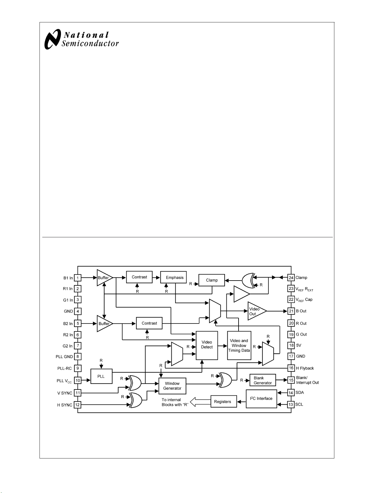
Block and Connection Diagram
Features
n Ideal companion IC to the LCCS to provide image
enhancing for viewing pictures or motion video
n Programmable clamp generator
n Programmable blank generator
n Video detection controlled by I
allowing easy and accurate Hi-Brite window calibration
n Programmable window Hi-Brite function
n Programmable image sharpness control (TV emphasis),
adjustable for different line rates
n Measures video position with respect to the horizontal
flyback and vertical sync pulses, providing necessary
information for auto-sizing
n Emphasis done either inside or outside the window
2
C compatible bus,
Applications
n Any monitor designed with the LCCS chip set
n Standard 0.7V video output assures compatibility with
any video pre-amp
2
C Compatible RGB Image Enhancer with Video Auto Sizing
20063501
FIGURE 1. Order Number LM1270N
See NS Package Number N24D
© 2003 National Semiconductor Corporation DS200635 www.national.com

Absolute Maximum Ratings (Notes 1,
3)
LM1270
If Military/Aerospace specified devices are required,
please contact the National Semiconductor Sales Office/
Distributors for availability and specifications.
Supply Voltage, Pins 9 and 18 6.0V
Peak Video Output Source Current
Thermal Resistance to Ambient (θ
Thermal Resistance to Case (θ
Junction Temperature (T
ESD Susceptibility (Note 4) 2 kV
ESD Machine Model (Note 5) 200V
Storage Temperature −65˚C to +150˚C
Lead Temperature (Soldering, 10 sec.) 265˚C
(Any One Amp) Pins 19, 20 or 21 28 mA
Voltage at Any Input Pin
(V
)V
IN
Power Dissipation (P
)
D
+0.5>V
CC
IN
(Above 25˚C Derate Based
and TJ) 2.4W
on θ
JA
>
−0.5V
Operating Ratings (Note 2)
Temperature Range 0˚C to +70˚C
Supply Voltage (V
Video Inputs 0.0V
CC
Active Video Signal Electrical Characteristics
Unless otherwise noted: TA= 25˚C, VCC= +5V, VIN= 0.7V, CL= 5 pF, Video Signal Output = 0.7V
Symbol Parameter Conditions
I
CC
I
CC-PS
LE Linearity Error Triangular Signal Input Source
V
O BLK TYP
V
O BLK A-B
V
O WHITE-MAX
t
r
OS
R
t
f
OS
F
f (−3 dB) Video Amplifier Bandwidth
V
10 kHz Video Amplifier 10 kHz Isolation (Note 14) −70 dB
SEP
V
10 MHz Video Amplifier 10 MHz Isolation (Note 14) −50 dB
SEP
A
V MAX
A
V 1/2
A
V MIN
A
V MATCH
A
V TRACK
VID
THRESHOLD
V
CLAMP MAX
V
CLAMP MIN
I
CLAMP LOW
Maximum Supply Current Both Supplies, RL=∞(Note 8) 165 235 mA
Maximum Supply Current, Power
Both Supplies, RL=∞(Note 8)
Save Mode
(Note 9)
Typical Video Black Level Output Test Setting 4, No AC Input Signal 1.2 1.4 1.6 VDC
Typical Video Black Level
No AC Input Signal
Difference A-B
White Level Video Output Voltage Video in = 0.7V 0.9 1.0 1.1 V
Rise Time 10% to 90%, AC Input Signal
(Note 10)
Overshoot (Rising Edge) AC Input Signal (Note 10) 6 %
Fall Time 90% to 10%, AC Input Signal
(Note 10)
Overshoot (Falling Edge) AC Input Signal (Note 10) 8 %
V
=1V
O
P-P
(Note 12)
Maximum Voltage Gain Reg. 09 & 0A = 7Fh, AC Input
Signal
Contrast@50% Level Reg. 09 & 0A = 40h, AC Input
Signal
Maximum Contrast Attenuation Reg. 09 & 0A = 00h, AC Input
Signal
Absolute Gain Match@A
V MAX
Reg. 09 & 0A = 7Fh, AC Input
Signal
Gain Change between Amplifiers Tracking When Changing A
(Note 11)
A
V 1/2
V MAX
Video Threshold Normal Operation 80 mV
Clamp Gate Low Input Voltage Default Mode, Clamp Comparators
Off
Clamp Gate High Input Voltage Default Mode, Clamp Comparators
On
Clamp Gate Input Current Default Mode, V24= 0V −1.6 −1.4 −1.1 mA
) 51˚C/W
JA
) 32˚C/W
JC
) 150˚C
J
& PLL VCC) 4.75V<V
.
P-P
Min
(Note 7)
Typ
(Note 6)
<
V
IN
Max
(Note 7)
CC
<
15 25 35 mA
5%
−0.05 0 0.05 VDC
1.9 ns
2.0 ns
200 MHz
1.3 1.4 1.5 V/V
−5 dB
−10 dB
±
0.5 dB
to
±
0.5 dB
2.2 V
2.8 V
<
1.0V
5.25V
P-P
Units
www.national.com 2
Active Video Signal Electrical Characteristics (Continued)
Unless otherwise noted: TA= 25˚C, VCC= +5V, VIN= 0.7V, CL= 5 pF, Video Signal Output = 0.7V
Symbol Parameter Conditions
I
CLAMP HIGH
t
PW CLAMP
t
CLAMP-VIDEO
V
CLAMP HIGH OUT
I
CLAMP HIGH OUT
V
CLAMP LOW OUT
I
CLAMP LOW OUT
R
IN-VIDEO
V
REFREXT
V
SPOT
Clamp Gate Input Current Default Mode, V24= 4V 0.5 0.7 0.9 mA
Back Porch Clamp Pulse Width Default Mode (Note 15) 200 ns
End of Clamp Pulse to Start of
Active Video
Default Mode, Limit Is Guaranteed
by Design
Clamp Gate High Output Voltage Internal Clamp Is Output at Pin 24 3.2 V
Clamp Gate High Output Current Internal Clamp Is Output at Pin 24 10 µA
Clamp Gate Low Output Voltage Internal Clamp Is Output at Pin 24 0.4 V
Clamp Gate Low Output Current Internal Clamp Is Output at Pin 24 −10 µA
Input Resistance 20 MΩ
V
REFREXT
Output Voltage 10 kΩ, 1% Resistor; Pin 23 to GND 1.26 1.44 1.64 V
Spot Killer Voltage VCCAdjusted to Activate 3.40 4.0 4.25 V
(Note 7)
Min
50 ns
.
P-P
Typ
(Note 6)
Max
(Note 7)
External Interface Signals Electrical Characteristics
Unless otherwise noted: TA= 25˚C, VCC= +5V, VIN= 0.7V, CL= 5 pF, Video Output = 0.7 V
Symbol Parameter Conditions
(I2C) I2C compatible Low Input Voltage SDA or SCL Inputs −0.5 1.5 V
V
L
V
(I2C) I2C compatible High Input Voltage SDA or SCL Inputs
H
(I2C) I2C compatible Low Input Current SDA or SCL, Input Voltage = 0.4V
I
L
I
(I2C) I2C compatible High Input Current SDA or SCL, Input Voltage = 4.5V
H
V
(I2C) I2C compatible Low Output Voltage IO= 3 mA 0.5 V
OL
I
IN THRESHOLD
I
IN-OPERATING
IINH-Flyback Detection Threshold −35 µA
Minimum —Insure Normal
Operation
Maximum —Should Not Exceed in
Lowest Operating Horizontal
Frequency in Given Application
(Note 15)
Normal Operation
I
IN FLYBACK
Peak Current during Flyback
Period, Recommended Design
Range
Operating Range for All Horizontal
Scan Frequencies, Maximum
Current Should Not Exceed 4 mA
(Note 15)
Note 1: Limits of Absolute Maximum Ratings indicate limits below which damage to the device must not occur.
Note 2: Limits of operating ratings indicate required boundaries of conditions for which the device is functional, but may not meet specific performance limits.
Note 3: All voltages are measured with respect to GND, unless otherwise specified.
Note 4: Human body model, 100 pF capacitor discharged through a 1.5 kΩ resistor.
Note 5: Machine Model ESD test is covered by specification EIAJ IC-121-1981. A 200 pF capacitor is charged to the specified voltage, then discharged directly into
the IC with no external series resistor (resistance of discharge path must be under 50Ω).
Note 6: Typical specifications are specified at +25˚C and represent the most likely parametric norm.
Note 7: Tested limits are guaranteed to National’s AOQL (Average Outgoing Quality Level).
Note 8: The supply current specified is the quiescent current for V
the supply current is used by the pre-amp.
Note 9: Linearity Error is the variation in step height of a 16 step staircase input signal waveform with a 0.7 V
with each step approximately 100 ns in width.
Note 10: Input from signal generator: t
generator response have been removed from the output rise and fall times.
Note 11: ∆A
gain change between any two amplifiers with the contrast set to A
gains might be 0.1 dB, −0.1 dB, and −0.2 dB and change to −5.2 dB, −4.9 dB and −4.7 dB respectively for contrast set to A
of −5.0 dB with a tracking change of
Note 12: Adjust input frequency from 10 MHz (A
Note 13: Measure output levels of the other two undriven amplifiers relative to the driven amplifier to determine channel separation. Terminate the undriven amplifier
inputs to simulate generator loading. Repeat test at f
Note 14: A minimum pulse width of 200 ns is guaranteed for a horizontal line of 15 kHz. This limit is guaranteed by design. If a lower line rate is used then a longer
clamp pulse may be required.
track is a measure of the ability of any two amplifiers to track each other and quantifies the matching of the three gain stages. It is the difference in
V
<
1 ns. Scope and generator response used for testing: tr= 1.1 ns, tf= 0.9 ns. Using the RSS technique the scope and
r,tf
±
0.2 dB.
max reference level) to the −3 dB corner frequency (f
V
= 10 MHz for V
IN
with RL=∞. Load resistors are not required and are not used in the test circuit, therefore all
CC
level at the input, subdivided into 16 equal steps,
P-P
and measured relative to the AVmax condition. For example, at AVmax the three amplifiers’
V 1/2
).
−3 dB
SEP 10 MHz
.
.
P-P
Min
(Note 7)
3.0
Typ
(Note 6)
Max
(Note 7)
VCC+
0.5
±
10 µA
±
10 µA
−50 µA
−550
2.0 3.0 4.0 mA
. This yields a typical gain change
V 1/2
LM1270
Units
Units
V
www.national.com3
External Interface Signals Electrical Characteristics (Continued)
Note 15: Limits met by matching the external resistor going to pin 24 to the H Flyback voltage.
LM1270
Typical Performance Characteristics
VCC= 5V, TA= 25˚C unless otherwise specified.
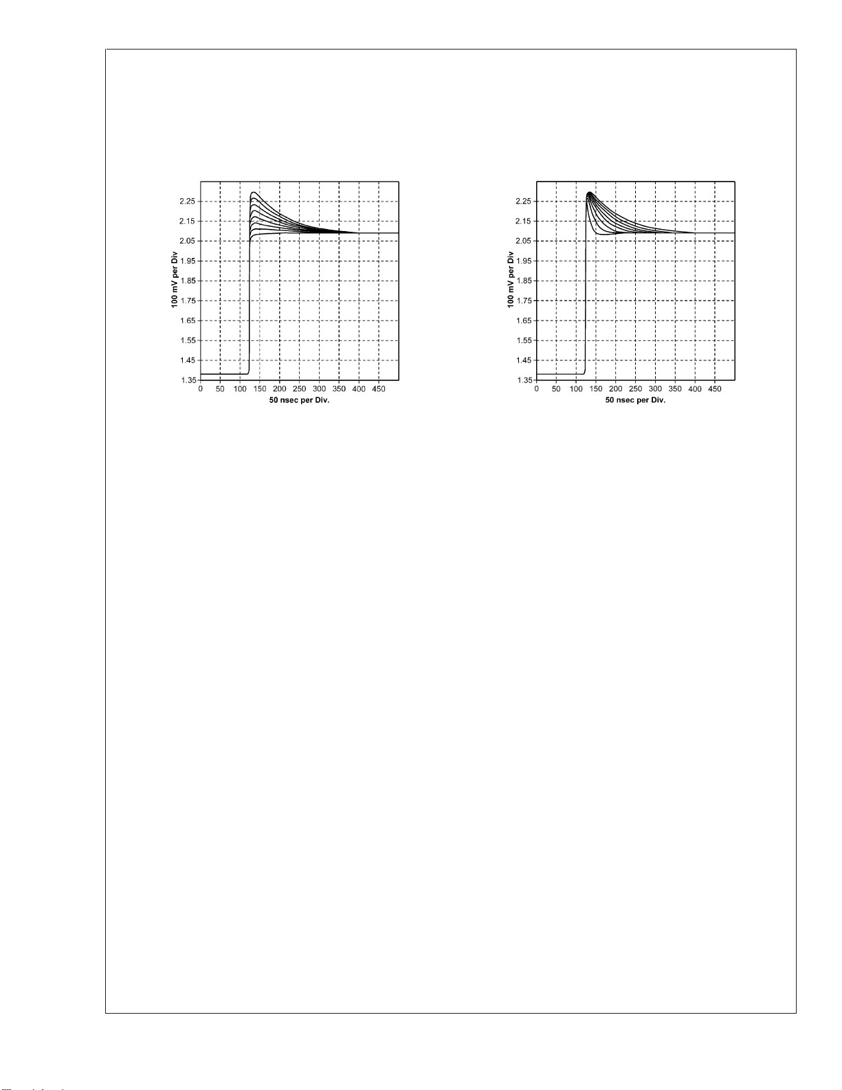
Emphasis, Center Frequency at Maximum Center Frequency, Emphasis at Maximum
20063502
The above two plots show the processing done by the
LM1270 on the video input signal. There are two variables
for the video processing, emphasis and center frequency.
Emphasis is controlled by bits 0-2 in register 0B. This gives
8 different levels of emphasis. In the above plot the center
frequency is set at its maximum level and the 8 different
levels of emphasis is measured. The output video with no
emphasis is adjusted to a 0.7 V
emphasis the video is increased to a 0.9 V
level. Using maximum
P-P
level at the
P-P
rising edge of the video. If the falling edge was measured it
would show a similar waveform, but going in the negative
direction.
Center frequency is shown in the second plot. Control of the
center frequency is done with bits 0-3 in register 0C. This
gives 16 adjustments for this feature. Every other adjustment
is shown in the above plot, showing all 16 adjustments would
have made the plot too hard to read. The curves closely
20063503
approximate the peaking of an RC network, therefore the
term center frequency means the RC time constant that is
approximated by each curve in the above plot. A true RC
peaking network would give very large overshoots. The
LM1270 has special circuitry to clip the very large overshoots, yet has the complete benefit of the RC peaking. This
special circuitry allows for much more overshoot than one
could do with RC peaking and still not saturate the video
channel.
Note that the video channel with the emphasis also has its
own independent contrast control. This allows the user to
adjust his monitor for a brighter picture within the Hi-Brite
window and optimize the emphasis for the resolution he is
using with the monitor. Now the user of the monitor can give
his pictures or video a special “sparkle” when using the
capabilities of the LM1270.
www.national.com 4
Pin Descriptions
LM1270
Pin
No.
1
2
3
Pin Name Schematic Description
Blue 1 Video In
Red 1 Video In
Green 1 Video In
4 Analog Input
Ground
5
Blue 2 Video In
6
Red 2 Video In
7
Green 2 Video In
Channel 1 video inputs. These inputs must be AC
coupled with a 0.1 µF cap. DC restoration is done at
these inputs. A series resistor of about 33Ω and
external ESD protection diodes should also be used.
Channel 1 video passes through the emphasis
section used for the Hi-Brite window. When using
Hi-Brite the channel 1 input pin must be shorted to
the corresponding channel 2 input pin.
Ground Pin for the input analog circuits of the
LM1270
Channel 2 video inputs. These video inputs must be
AC coupled with a 0.1 µF cap. DC restoration is
done at these inputs. A series resistor of about 33Ω
and external ESD protection diodes should also be
used. When using Hi-Brite the channel 2 input pin
must be shorted to the corresponding channel 1
input pin.
810Digital Ground
PLL V
CC
9 PLL Filter
11 V Sync
The ground pin should be connected to the rest of
the circuit ground by a short but independent PCB
trace to prevent contamination by extraneous
signals. The V
rest of the V
pin should be isolated from the
CC
line by a ferrite bead and bypassed
CC
to pin 8 with an electrolytic capacitor and a high
frequency ceramic.
Recommended topology and values are shown to
the left. It is recommended that both filter branches
be bypassed to the independent ground as close to
pin 8 as possible. Great care should be taken to
prevent external signals from coupling into this filter
2
from video, I
C compatible bus, etc.
Logic level vertical sync signal received from the
video card in the PC or sync stripper circuit.
www.national.com5
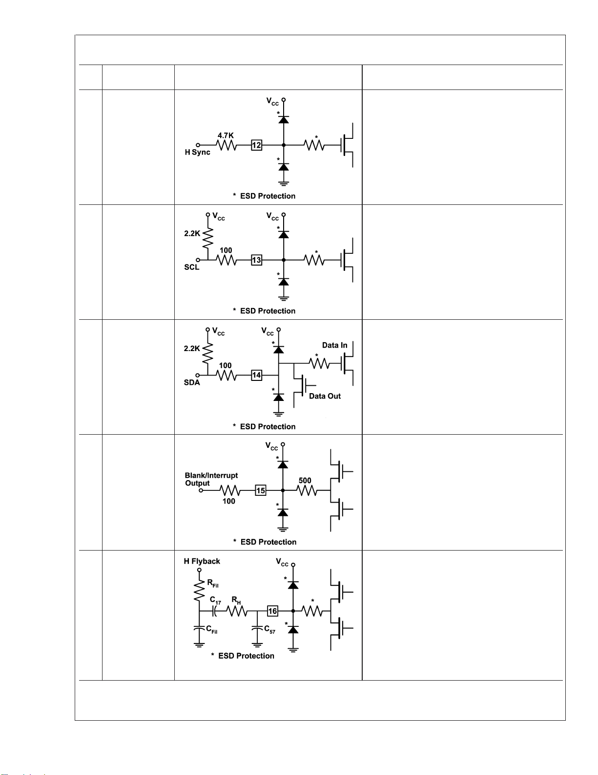
Pin Descriptions (Continued)
LM1270
Pin
No.
12 H Sync Logic level horizontal sync signal received from the
Pin Name Schematic Description
video card in the PC or sync stripper circuit.
13 SCL
14 SDA
15 Blank/Interrupt
Out
The I2C compatible Clock line. A pull-up resistor of
about 2 kΩ should be connected between this pin
and V
. A 100Ω resistor should be connected in
CC
series with the clock line for additional ESD
protection.
The I2C compatible data line. A pull-up resistor of
about 2 kΩ should be connected between this pin
and V
. A 100Ω resistor should be connected in
CC
series with the data line for additional ESD
protection.
This output pin can be selected for Vertical Blank,
blank all the video, or no blanking. Provides the
blanking signal normally used at G1 of the CRT,
blanking the video during vertical retrace. If blanking
is not required, this pin may be used as an interrupt
signal for the microcontroller.
16 H Flyback
www.national.com 6
Proper operation requires current reversal. R
H
should be large enough to limit the peak current at
pin 16 to about +2 mA during blanking, and
−300 µA during scan. C
is usually needed for logic
17
level inputs and should be large enough to make
the time constant, R
horizontal period. R
significantly larger than the
HC17
Fil
and C
are typically 300Ω
Fil
and 330 pF when the flyback waveform has ringing
and needs filtering. These two parts are not used on
the current neck board. C
may be needed to filter
57
extraneous noise and can be up to 100 pF.
Pin Descriptions (Continued)
LM1270
Pin
No.
Pin Name Schematic Description
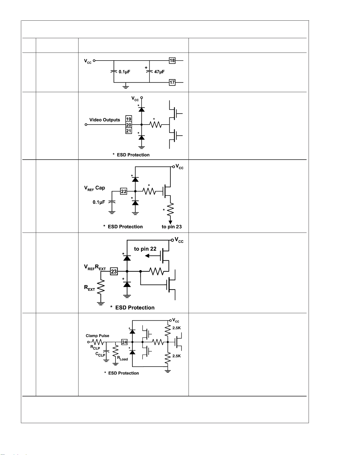
1718Ground
V
CC
19
Green Video Out
20
Red Video Out
21
Blue Video Out
22 V
REF
Ground pin for the output analog portion of the
LM1270 circuitry, and power supply pin for all the
analog of the LM1270. Note the recommended
charge storage and high frequency capacitors which
should be as close to pins 17 and 18 as possible.
Video outputs of the LM1270. Typically the output is
set to 0.7 V
to drive any standard video pre-amp.
P-P
When Hi-Brite is activated the user can set the
video output as high as 1.0 V
P-P
.
Cap Provides filtering for the internal voltage which sets
the internal bias current in conjunction with R
EXT
.A
minimum of 0.1 µF is recommended for proper
filtering. This capacitor should be placed as close to
pin 22 and the analog ground return as possible.
This pin can also be set to use an external V
REF
.
23 V
REFREXT
24 Clamp
Sets the internal current sources through a
10 kΩ 1% external resistor. Resistor value and
accuracy is critical for optimum operation of the
LM1270. This resistor should be placed as close to
pin 23 and the analog ground return as possible.
This pin can either accept an external clamp pulse
or send an internally generated clamp pulse to the
video circuits. As an input this pin accepts either
TTL or CMOS logic levels. The internal switching
threshold is approximately one-half of V
external series resistor, R
, of about 1 kΩ is
CLP
CC
.An
recommended to avoid overdriving the input
devices, or for current limiting the drivers if being
used as an output. C
filtering noise on the clamp input. R
may be necessary for
CLP
LOAD
should be
used if this pin is an output with a value of about
10 kΩ.
www.national.com7
Functional Description
LM1270
VIDEO SECTION
The LM1270 gives the monitor designer the ability to add a
highlighted window to the CRT monitor. Special software
provided manufacturer enables the user to select the area
he wants to have highlighted. National Semiconductor refers
to this feature as Hi-Brite. Referring to Figure 1, the Block
Diagram of the LM1270, note that there are two channels for
each video input. Of the three video channels only the blocks
of the blue channel are shown since all three channels have
the same blocks. A buffer stage is located at the video inputs
and this is followed by a contrast control. Referring to channel one (B1 input), the contrast control is followed by an
emphasis block. The combination of the emphasis control
and the contrast control gives the desired highlighted video
inside the Hi-Brite window. The output of the emphasis stage
and the output of the contrast control in channel two go to a
high-speed video switch, which selects the video channel
going to the output stage.
Having an independent contrast control in each video channel allows the user to adjust the video gain, normally having
the higher gain in channel one, giving a “brighter” picture
within the Hi-Brite window. The Emphasis stage is used to
give more “sparkle” to the highlighted video. Video going into
the emphasis stage has peaking added to the video. Both
the amplitude and the duration of the peaking are adjustable
through the I
different video resolutions. Maximum peaking is 20%. Although most uses of the Hi-Brite would be for the video
inside the selected window, the reverse may be selected
where all the video outside the window is processed through
the emphasis stage. Please remember that for all video
inputs the corresponding channel one input and the channel
two input must be shorted together. Standard AC coupling
such as used with the LM123X or LM124X pre-amps is to be
used with the LM1270.
2
C COMPATIBLE INTERFACE
I
Pins 13 and 14 receive signals from an I
The interface section is used to decode the I
signal and update the registers. Note that all functions of the
LM1270 are controlled through an I
bus. Details on the internal registers are covered in the I
compatible Interface Registers Section.
PLL
A phase locked loop (PLL) is required for the LM1270 to sync
all the timing circuits to the incoming horizontal sync. Proper
operation of both the Hi-Brite window and the video detection requires a proper lock of the PLL reference pulse to the
horizontal sync. Careful layout of the loop filter at pin 10 is
necessary for keeping noise out of the PLL section. The
register to the PLL is used to set the number of pixels per line
for the internal counters that set the Hi-Brite window, generate the internal clamp pulse, and set the counters for the
video detection. The maximum number of pixels per line is
2,047, or 7Fh. For good resolution of the window, 640 is the
recommended minimum pixels per line. The VCO has a
running frequency range of 110 MHz to 160 MHz when using
prescaler 7. For the other pre-scaler settings the frequency
range is 120 MHz to 220 MHz. The output of the VCO goes
to a pre-scaler with a 3 bit register, dividing the VCO output
by up to 8. Minimum division is 1, just a straight pass through
the pre-scaler. Calculating the VCO frequency:
F
VCO
2
C compatible bus, optimizing the emphasis for
2
C compatible bus.
2
CoranI2C compatible
= VCO frequency
2
C compatible
F
= Horizontal line frequency
H
N = Number of pixels per line
M = PLL pre-scaler
Using the above terms gives the following formula for the
PLL:
=N*M*F
F
VCO
H
It is easiest to run the PLL in AUTO mode, setting bit 7 of
address 0E to a “1”. Here the user programs in the desired
pixels per line and the part will select the preferred pre-scaler
number. If one is using manual mode below is a table
showing the relationship between the pre-scaler and the
VCO frequency. The chart shows the pixel frequency, F
F
P=FVCO
/M
.
P
The necessary pixels per line is calculated by the following
formula:
N=F
P/FH
PRESC2PRESC2PRESC2PRES
DIV RATIO
FP(max)
MHz
Fp(min)
MHz
1 1 1 1 160.0 110.0
1 1 0 2 110.0 60.0
1 0 1 3 73.3 40.0
1 0 0 4 55.0 30.0
0 1 1 5 44.0 24.0
0 1 0 6 36.7 20.0
0 0 1 7 31.4 17.1
0 0 0 8 27.5 10.0
TIMING AND WINDOW GENERATION SECTION
All timing is referenced to the vertical and horizontal sync
inputs that come in on pins 11 and 12 respectively. The two
registers near the inputs sets the start of the window for both
the horizontal and vertical direction. The window generator
and the following logic are used to generate a pulse to
control the video switch used to switch between the video
with emphasis and the standard video. The switching between the two video channels is the generation of the window seen by the user. There is the option to switch off the
Hi-Brite window. An additional switch located just before the
2
C
video switch is used to turn off the control signal.
Video detection is another important function inside the
LM1270. Note that both video channels, the PLL, and both
vertical sync and horizontal flyback signals all go to this
block. From these inputs the video detection is used to
detect the length of the horizontal and vertical front porch as
well as the length of the active video for both the horizontal
and vertical directions. This information allows the monitor
designer to offer auto alignment in his monitor. Further processing of the video information in the video and window
timing data section generates an internal clamp pulse. This
is the DC restoration pulse for the LM1270. Pin 24 is the
output for the clamp pulse, allowing the monitor designer to
use it for the clamp input of the pre-amp. There is also the
option to program the LM1270 to accept an external clamp
pulse instead of using its own internally generated pulse.
The video detection section also has a data receiver for
receiving data encoded on the video. When this feature is
used, the MCU in the monitor is used to control the LM1270,
keeping all communication with the LM1270 within the monitor. This results in a faster response time by eliminating the
need for the computer to control the LM1270. Control by the
computer requires communication through the monitor MCU.
www.national.com 8
Functional Description (Continued)
Using the data encoded on the video eliminates one stage of
communicating with the LM1270, allowing for a faster response time for changes in the Hi-Brite window.
V
REF
Proper operation of the LM1270 does require a very accurate reference voltage. This voltage is generated in the V
block. To insure an accurate voltage over temperature, an
external resistor is used to set the current in the V
The external resistor is connected to pin 23. This resistor
should be 1% and have a temperature coefficient under
100 ppm/˚C. ALL VIDEO SIGNALS MUST BE KEPT AWAY
FROM PIN 23. This pin has a very high input impedance and
will pick up any high frequency signals routed near it. The
board layout shown in Figure 12 is a good example of trace
routing near pin 23. The output of the V
stage goes to a
REF
number of blocks in the video section and also to pin 22. This
pin allows capacitor filtering on the V
output and offers an
REF
accurate external reference. A buffer must be used with this
reference, the maximum current loading should be only
100 µA. Pin 22 is bi-directional, allowing the LM1270 to be
referenced to a pre-amp V
. This configuration makes it
REF
possible to DC couple to the pre-amp, but for accurate DC
level, it is recommended that AC coupling be used between
the LM1270 and the pre-amp. It is also recommended that
the internal V
be used for best performance. Note: Any
REF
noise injected into pin 22 will appear on the video. The
voltage reference must be kept very clean for best performance of the LM1270.
REF
REF
stage.
LM1270
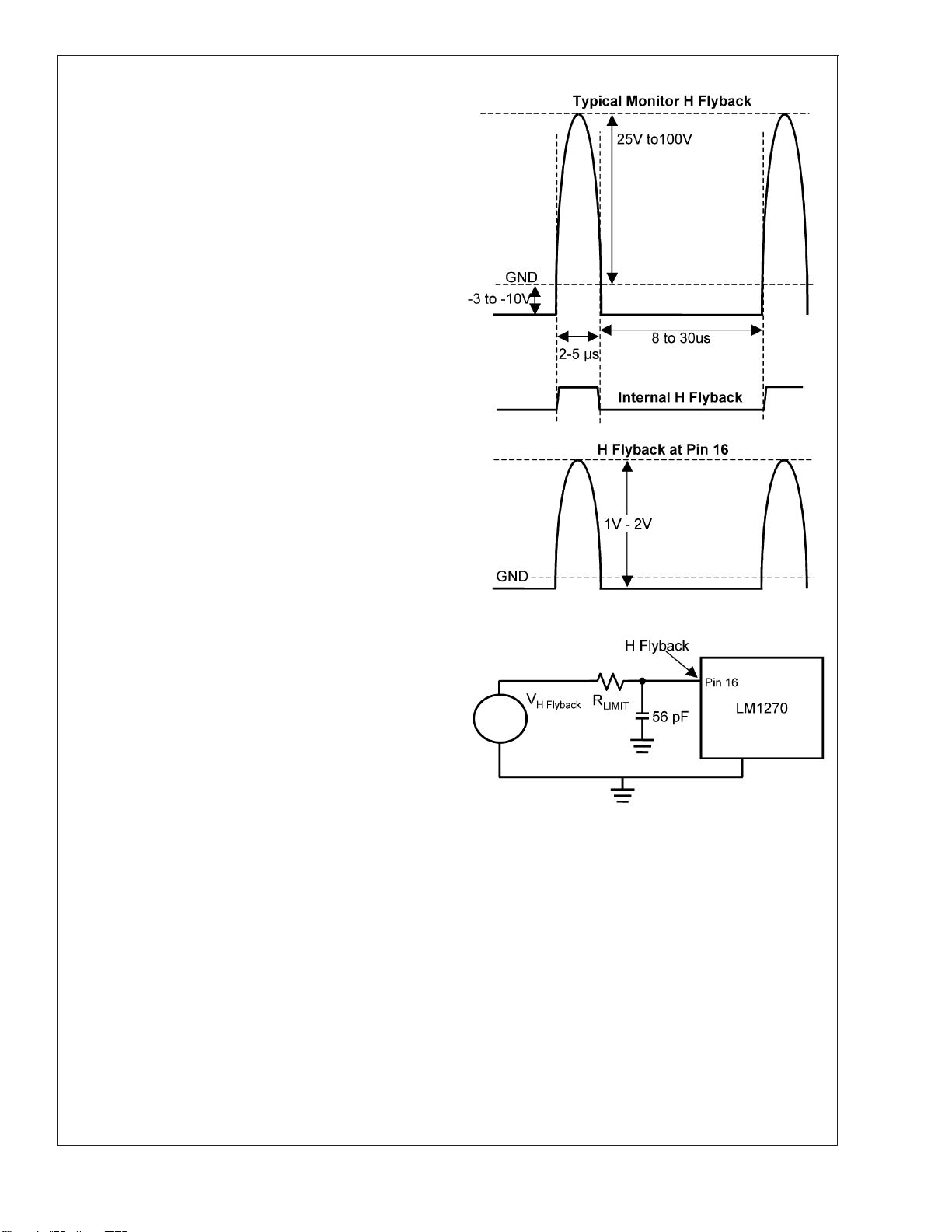
H FLYBACK
H Flyback is an analog signal input from the monitor horizontal scan. This flyback signal goes to the internal horizontal flyback pulse generation circuit. An optional capacitor
and/or resistor to ground may be needed if noise interferes
with the H Flyback signal or if there is ringing on the H
Flyback signal. Note: there is no blanking pedestal on the
output video. If horizontal blanking is to be added to the
video signal it must be done at the pre-amp.
is used to limit the input current into the IC to a
R
LIMIT
maximum value of +1 mA during flyback and −100 µA during
normal forward scan. For example if an H flyback with a peak
of 100V is used, R
= 100 kΩ. The internal input imped-
LIMIT
ance of pin 16 is low to limit the maximum voltage swing at
the input to be within the supply rail and ground. Figure 2
shows the H flyback waveforms and the location of R
LIMIT
.A
56 pF capacitor has been added to the H Flyback pin for
filtering noise on the H Flyback signal.
20063519
FIGURE 2. H Flyback Input Pulse
VERTICAL BLANKING
A similar vertical pulse generation circuit to the LM1238 is
included internal to the LM1270. The leading edge of the
vertical sync is used to start the programmable vertical
blanking signal directly. The Vertical Blank Duration Control
Register sets the width of the pulse. When vertical blanking
is enabled its polarity is programmable.
CLAMPING
Pin 24, the clamp pin, can be set for either an input or and
output. If used as an input, then this pin functions just like the
clamp input pins to the video pre-amps. One should use a
series 1 kΩ resistor to pin 24 and a small capacitor may also
be needed between pin 24 and ground to filter high frequency noise.
www.national.com9

Functional Description (Continued)
The LM1270 has the counters required to locate the clamp
LM1270
pulse to any position on the horizontal line. Normally this pin
would be used as an output and be connected to the video
pre-amps. Now the clamp pulse location can be optimize for
the video channel. Note: When using this pin as an output a
1kΩ series resistor must be used to protect the output stage
of the clamp circuit. It is also recommended to connect a
10 kΩ resistor between this pin and ground for more reliable
operation.
Video Detection
MODES OF OPERATION
Three modes of operation are possible with the video detect
circuit:
1. Autosizing mode: in this mode the LM1270 takes the
measurements necessary for the monitor to perform the
autosizing operation. The horizontal flyback is used as
the reference for timing. The resultant horizontal outputs
are the flyback time, the position of the start of video
relative to the flyback end and the time from the end of
the active video to the start of the flyback time. Since the
total line time is known the microcontroller can calculate
the active video time. Now the microcontroller can center the video between the start and end of flyback for
best image centering, and to calculate the duty cycle of
the video with respect to the forward scan time, thus
giving a measure of the relative size of the image. For
best performance in autosizing mode, it is recommended that the maximum pixels per line mode is used
when measurements are made.
2. Window calibration mode: in this mode, the horizontal
sync is used as the reference for timing. The resultant
horizontal outputs are the horizontal sync time and the
back porch and active image video time that can subsequently be used in conjunction with the image position
data. The image pixel per line value should be used to
set the PLL.
3. Video data transfer: in this mode, data is sent from the
PC to the monitor on the first active video line. A 72 pulse
clock string is sent on one video channel. Data is sent on
a second video channel. A window signal that tracks the
actual highlight window is sent on the third video channel. The timing parameters of this window signal are
timed by the video detect logic and stored in a special
register set. The relationship between these three signals is shown in Figure 3.
The selection of which video channel contains which signal
is programmed by the D_CNTL register.
20063520
FIGURE 3. Data, Clock and Window Signals
IMAGE CALIBRATION MODE
Two registers are used for each axis to control the window
enable signal, WIN_EN. The first register HW_START
(VW_START) defines the period in pixels (lines) from the
leading edge of the Hsync (Vsync) to the start of the window.
The second register HW_END (VW_END) defines the duration of the highlight window. Each of these registers is defined as two byte values, as per the table below:
The microcontroller must write the values of these registers,
after it has received the window position information from the
PC. However, the PC may reference this information in any
of the following ways:
1. Leading edge of sync
2. Trailing edge of sync
3. Start of the video image
In order to accommodate different modes of operation, the
video detect function may be used to measure the sync
width, and the back porch (i.e., trailing edge of sync to start
of video) periods in horizontal pixels, or vertical lines for
window position calibration. The video detect function must
be set to measure with reference to the horizontal sync.
If the leading edge of sync is used as the reference for the
window start timing from the PC application, then the start
values can be directly written to the registers HW_START
and VW_START.
If the trailing edge of sync is used as the reference for the
window start timing from the PC application, then the microcontroller should add the measured sync durations from the
video detect registers to the timing values supplied by the
PC application before writing to the HW_START and
VW_START registers.
If the start of video image is used as the reference for the
window start timing from the PC application, then the microcontroller will add the measured sync duration and the back
porch duration from the video detect registers to the timing
values supplied by the PC application before writing to the
HW_START and VW_START registers.
In each case, it may also be necessary to modify the window
position values by adding or subtracting a value to compen-
www.national.com 10

Video Detection (Continued)
sate for clocking delays in the timing counters in the
LM1270. This value is empirically derived from testing the
video system.
VIDEO INPUT DETECTION
The outputs of the three video detector channels are OR’d
together to provide a single composite signal of the three
channels when used for timing parameter measurement.
The video detect logic must find the extreme points of the
displayed image during each frame with respect to the horizontal and vertical flyback pulses as measured using the
internal PLL. For best performance in autosizing mode, it is
recommended that the application use the maximum number
of pixels per line when measurements are made. Remember, the VCO frequency is limited to 160 MHz when the
prescaler is set to 7.
The durations to be measured are shown generically in the
figures below, and apply to both horizontal and vertical timings. For the horizontal timings the measurements will depend on the mode selected in the EMPHASIS register. Vertical and HFLYBACK timing measurements will be the same
in both modes.
1. Flyback or sync period: the duration of either the sync
input or the horizontal flyback, in either horizontal lines
(vertical) or pixels (horizontal).
2. Back porch period: the duration between the trailing
edge of the sync or flyback pulse and the leading edge
of the first detected video, in either lines (vertical) or
pixels (horizontal).
3. Video period: the duration between the leading edge of
the first detected video and the trailing edge of the last
detected video, in either lines (vertical) or pixels (horizontal).
4. Front porch: the duration between the trailing edge of
the last detected video and the leading edge of the sync
or flyback pulse, in either lines (vertical) or pixels (horizontal).
Note: In the horizontal timing measurement description, reference to sync
means either HSYNC or H_FEEDBACK, selected by WCHE bit in the
EMPHASIS register.
As the video may start and finish at different positions on the
screen, depending upon the image, the measured horizontal
porches and video time may vary from line to line. To overcome this, the periods should be measured over at least one
entire field. The hardware records the shortest back porch
and front porch periods used over the measured period.
WINDOW COORDINATE DATA
The microcontroller must program the highlight window coordinates in the LM1270 by writing to the appropriate registers. The coordinate values must be sent from the PC. For
maximum flexibility, the LM1270 is designed to allow operation such that the coordinate data may be sent by:
2
1. DDC2A/B (e.g., I
C compatible) transmission
2. Information carried as video data during the vertical
blanking time
3. Any other PC-monitor interface (e.g., USB)
LM1270
FIGURE 4. Timing Intervals with WCHE = 1
FIGURE 5. Timing Intervals with WCHE = 0
20063521
20063522
COORDINATE DATA TRANSMISSION BY VIDEO
OPERATION
When sending coordinate data by video please refer to the
information for register 27 in the register descriptions. Any
video line may be selected for data, clock, or window. It is
important to make sure each video line has a different selection otherwise the video transmission of data will not
function. It is possible to program two video channels to
carry the same information and create this incorrect operation.
If the LIMIT bit of the TEST1 register is set to a “1” (default
value), then one line of data may be transmitted after the
vertical sync on one of the video channels. This data must be
sent during the vertical blanking time that is set by the
vertical blanking register. Data must be transmitted only
during the vertical blanking time otherwise it will be ignored
by the logic. If the LIMIT bit of the TEST1 register is set to a
“0”, then the data may be transmitted at any time following
the vertical sync.
The data consists of a stream of 9 bytes. In normal use it is
expected that the first eight bytes will be data, and the
remaining byte will be used as a checksum. Alternatively, the
ninth byte may be used as an additional data byte.
Another video channel provides a clock pulse stream of
exactly 72 pulses. The logic counts the number of pulses
between two horizontal sync pulses. If the number of clock
pulses is greater or less than 72, then the data is ignored. If
the count is 72, then the data is shifted into registers 2E-36
upon arrival of the next horizontal sync, provided the output
www.national.com11

Video Detection (Continued)
registers have been enabled either by previously reading the
LM1270
D_CNTLS register, or by writing a zero to the STAT bit of the
D_CNTL register.
Only one line of data is allowed per field. After the clock
stream of 72 pulses has been detected and accepted and
the data stored in registers 2E-36, no more data will be
accepted until after the registers have been reset. This is to
allow time for the microcontroller to access the data on the
2
C bus. If the LIMIT bit in the TEST1 register is set to a “1”
I
(default value), then the data must arrive during the programmed vertical blanking period. Any data arriving outside
of this will be ignored. If the bit is set to a “0”, then the data
may arrive anytime, even within the active video area.
The maximum data rate is half of the clock rate. The data is
clocked by the trailing edge of the clock. The clock rate
should be chosen to allow all 72 pixels to occur within the
normal horizontal active video timing.
INTERRUPT SIGNAL
Pin 15, the Blanking/Interrupt pin, can be set to output an
interrupt signal by bit 2 of register 39. The default value for
this bit is “0”, setting pin 15 for a blanking output signal.
However, if bit 2 is set to a “1” then pin 15 outputs an
interrupt signal. When the LM1270 is instructed to read the
information sent by video, then this signal goes low. Once
the clock stream of 72 pulses has occurred, then the interrupt signal goes high again at the leading edge of H Sync.
The interrupt signal remains high until another request to
read the video information is received. Some microcontrollers may require an interrupt signal. Setting pin 15 to output
an interrupt signal will provide the needed signal for these
systems. In this mode of operation the vertical blanking
signal will be unavailable; however, vertical blanking may still
be added to the video outputs. Note that bit 1 of register 1
does change the polarity of the interrupt signal.
Parameter Timing
T
CLK
T
CLK-H
T
CLK-L
T
SETUP-H
T
SETUP-L
50 ns
25 ns
25 ns
13 ns
13 ns
Emphasis
MEASURING EMPHASIS
Two adjustments are available to optimize the emphasis in
the Hi-Brite window for the various timing modes and brightness levels. One adjustment is the center frequency and the
other adjustment is the amount of overshoot. Referring to
Figure 7 the overshoot is the ratio of the overshoot voltage to
the video level after the emphasis has settle out of the output
signal. The typical output level is 900 mV and the typical
overshoot is about 20%. The peak measurement is taken
9 ns from the rising edge. This delay gives a more accurate
peak measurement by avoiding any ringing that may occur
at the rising edge. Overshoot is defined in percent as:
FIGURE 6. Timing Parameters
20063525
FIGURE 7. Overshoot Measurement
Bits 0 to 2 in register 0B control the emphasis. When a “4” is
programmed into these bits the overshoot is typically 11%. A
“0” will give no overshoot in the Hi-Brite window.
Shown below in Figure 8 is how the center frequency is
measured. The center frequency is actually expressed as
the time it takes the overshoot to settle to within 5% of the
DC level of the pulse.
20063526
20063523
FIGURE 8. Center Frequency Measurement
www.national.com 12

Emphasis (Continued)
Bits 0 to 3 in register 0C control the center frequency. When
an “8” is programmed into the register the t
typically 80 ns. An “F” will give about 145 ns. A “0” will give no
emphasis in the Hi-Brite window.
Center Freq
ESD and Arc-Over Protection
The LM1270 incorporates full ESD protection with special
consideration given to maximizing arc-over robustness. The
monitor designer must still use good circuit design and PCB
layout techniques. The human body model ESD susceptibility of the LM1270 is 3.5 kV, however, many monitor manufacturers are now testing their monitors to level 4 of the IEC
801-2 specification which requires the monitor to survive an
8 kV discharge. External ESD protection is needed to survive this level of ESD. The LM1270 provides excellent protection against both ESD and arc-over, but this is not a
substitute for good PCB layout.
Figure 9 shows the recommended input protection for the
LM1270. This provides the best protection against ESD.
When this protection is combined with a good PCB layout
the LM1270 will easily survive the IEC 801-2 level 4 testing
(8 kV ESD). It is strongly recommended that the protection
diodes be added as shown in Figure 9. The 1N4148 diode
has a maximum capacitance of 4 pF which will have little
effect on the response of the video system due to the low
impedance of the input video.
The ESD cells of the LM1270 also provide good protection
against arc-over, however good PCB layout is necessary.
The LM1270 should not be exposed directly to the voltages
that may occur during arc-over. The main vulnerability of the
LM1270 to arc-over is through the ground traces on the
PCB. For proper protection all ground connections associated with the LM1270, including the grounds to the bypass
capacitors, must have short returns to the ground pins. A
significant ground plane should be used to connect all the
LM1270 grounds. Figure 12, which shows the demo board
LM1270
layout, is an excellent example of an effective ground plane.
Figures 10, 11 are the schematic to the demo board. The list
below should be followed to ensure a PCB with good
is
grounding:
All grounds associated with the LM1270 should be con-
•
nected together through a large ground plane.
CRT driver ground is connected to the LM1270 and video
•
pre-amp ground area at one point.
CRT and arc protection grounds are connected directly to
•
the chassis or main ground. There is no arc-over current
flow from these grounds through the LM1270 grounds.
Input signal traces for SDA, SCL, H Flyback, and Sync
•
inputs should be kept away from the CRT driver and all
traces that could carry the arc current.
Output signal traces of the LM1270 should be kept away
•
from the traces that carry the output signals of the CRT
driver.
If any one of the above suggestions is not followed the
LM1270 may become more vulnerable to arc-over. Improper
grounding is by far the most common cause of a video
pre-amp failure during arc-over.
20063527
FIGURE 9. Recommended Video Input ESD Protection
www.national.com13

LM1270
FIGURE 10. LM1270, LM1237/47, LM2465 Neck Board, Page 1
www.national.com 14
20063528

LM1270
FIGURE 11. LM1270, LM1237/47, LM2465 Neck Board, Page 2
20063529
www.national.com15

LM1270
FIGURE 12. LM1270, LM1237/47, LM2465 Neck Board
www.national.com 16
20063530

Microcontroller Interface
The microcontroller interfaces to the LM1270 pre-amp via an
C compatible interface. The protocol of the interface begins
I
2
with the Start Pulse followed by a byte comprised of a
seven-bit Slave Device Address and a Read/Write bit as the
LSB. Therefore the address of the LM1270 for writing is 54h
(0101 0100) and the address for reading is 55h (0101 0101).
Figures 13, 14 show a write and read sequence across the
2
C compatible interface.
I
WRITE SEQUENCE
The write sequence begins with a start condition which
consists of the master pulling SDA low while SCL is held
high. The slave device address is sent next. The address
byte is made up of an address of seven bits (7–1) and the
read/write bit (0). Bit 0 is low to indicate a write operation.
Each byte that is sent is followed by an acknowledge. When
SCL is high the master will release the SDA line. The slave
must pull SDA low to acknowledge. The address of the
register to be written to is sent next. Following the register
address and the acknowledge bit the data for the register is
sent. If bit 0 of register 0Ah is set low (default value) then the
LM1270 is set for the increment mode. In this mode when
more than one data byte is sent it is automatically incremented into the next address location. See Figure 13. Note
that each data byte is followed by an acknowledge bit.
READ SEQUENCE
2
Read sequences are comprised of two I
C compatible transfer sequences: The first is a write sequence that only transfers the address to be accessed. The second is a read
sequence that starts at the address transferred in the previous address write access and incrementing to the next address upon every data byte read. This is shown in Figure 14.
The write sequence consists of the Start Pulse, the Slave
Device Address including the Read/Write bit (a zero, indicating a write), then its Acknowledge bit. The next byte is the
address to be accessed, followed by its Acknowledge bit and
the Stop bit indicating the end of the address only write
access.
Next the read data access is performed beginning with the
Start Pulse, the Slave Device Address including the Read/
Write bit (a one, indicating a read) and the Acknowledge bit.
The next 8 bits will be the data read from the address
indicated by the write sequence. Subsequent read data
bytes will correspond to the next increment address locations. Each data byte is separated from the other data bytes
by an Acknowledge bit.
LM1270
FIGURE 13. I2C Compatible Write Sequence
20063531
www.national.com17

Microcontroller Interface (Continued)
LM1270
20063532
FIGURE 14. I2C Compatible Read Sequence
I2C Compatible Interface Registers
IC ADDRESS for I2C Compatible Bus
Slave Address of the LM1270 is 54h when writing to the registers and 55h when reading from the registers.
REGISTER ADD DEFLT 76543210
I_O0 00 00 VDT HSY/FB RESET BLACK VCLB PWRSV SEL/WB A/B_SEL
I_O1 01 08 CL POL CL I/O BL POL BLANK VBL EN RSV VSY POL HSY POL
CL_POS0 02 00 CLP7 CLP6 CLP5 CLP4 CLP3 CLP2 CLP1 CLP0
CL_POS1 03 00 CLP9 CLP8
CL_DUR 04 04 CLD7 CLD6 CLD5 CLD4 CLD3 CLD2 CLD1 CLD0
Not Used 05 00 RSV RSV RSV RSV RSV RSV RSV RSV
Not Used 06 00 RSV RSV
Not Used 07 00 RSV RSV RSV RSV RSV RSV RSV RSV
V_BL_DU 08 0F VB6 VB5 VB4 VB3 VB2 VB1 VB0
ACONT 09 52 RSV ACON6 ACON5 ACON4 ACON3 ACON2 ACON1 ACON0
BCONT 0A 52 RSV BCON6 BCON5 BCON4 BCON3 BCON2 BCON1 BCON0
EMPHASIS 0B 00 WIN_SEL VREF WCHE WGHE RSV EMP2 EMP1 EMP0
CNT_F 0C 08 CENTF3 CENTF2 CENTF1 CENTF0
PPL0 0D FF PPL7 PPL6 PPL5 PPL4 PPL3 PPL2 PPL1 PPL0
PS_PPL1 0E 7F AUTO PRESC2 PRESC1 PRESC0 FRERUN PPL10 PPL9 PPL8
HW_ST0 0F 00 HW_ST7 HW_ST6 HW_ST5 HW_ST4 HW_ST3 HW_ST2 HW_ST1 HW_ST0
HW_ST1 10 00 HW_ST10 HW_ST9 HW_ST8
HW_END0 11 00 HW_EN7 HW_EN6 HW_EN5 HW_EN4 HW_EN3 HW_EN2 HW_EN1 HW_EN0
HW_END1 12 00 HW_EN10 HW_EN9 HW_EN8
VW_ST0 13 00 VW_ST7 VW_ST6 VW_ST5 VW_ST4 VW_ST3 VW_ST2 VW_ST1 VW_ST0
VW_ST1 14 00 VW_ST10 VW_ST9 VW_ST8
VW_END0 15 00 VW_EN7 VW_EN6 VW_EN5 VW_EN4 VW_EN3 VW_EN2 VW_EN1 VW_EN0
www.national.com 18

I2C Compatible Interface Registers (Continued)
REGISTER ADD DEFLT 76543210
VW_END1 16 00 VW_EN10 VW_EN9 VW_EN8
H_FP0 17 FF HFP7 HFP6 HFP5 HFP4 HFP3 HFP2 HFP1 HFP0
H_FP1 18 07 HFP10 HFP9 HFP8
HF_S0 19 FF HFL_HS7 HFL_HS6 HFL_HS5 HFL_HS4 HFL_HS3 HFL_HS2 HFL_HS1 HFL_HS0
HF_S1 1A 03 HFL_HS9 HFL_HS8
H_BP0 1B FF HBP7 HBP6 HBP5 HBP4 HBP3 HBP2 HBP1 HBP0
H_BP1 1C 07 HBP10 HBP9 HBP8
V_FP0 1D FF VFP7 VFP6 VFP5 VFP4 VFP3 VFP2 VFP1 VFP0
V_FP1 1E 07 VFP10 VFP9 VFP8
V_SYN_D 1F FF VSYNC7 VSYNC6 VSYNC5 VSYNC4 VSYNC3 VSYNC2 VSYNC1 VSYNC0
V_BP0 20 FF VBP7 VBP6 VBP5 VBP4 VBP3 VBP2 VBP1 VBP0
V_BP1 21 07 VBP10 VBP9 VBP8
V_FP0_PRV 22 FF VFP7 VFP6 VFP5 VFP4 VFP3 VFP2 VFP1 VFP0
V_FP1_PRV 23 07 VFP10 VFP9 VFP8
V_SYN_D_PRV 24 FF VSYNC7 VSYNC6 VSYNC5 VSYNC4 VSYNC3 VSYNC2 VSYNC1 VSYNC0
V_BP0_PRV 25 FF VBP7 VBP6 VBP5 VBP4 VBP3 VBP2 VBP1 VBP0
V_BP1_PRV 26 07 VBP10 VBP9 VBP8
D_CNTL 27 00 STAT WD G1 G0 B1 B0 R1 R0
HW_SM0 28 00 HWSM7 HWSM6 HWSM5 HWSM4 HWSM3 HWSM2 HWSM1 HWSM0
HW_SM1 29 00 HWSM10 HWSM9 HWSM8
HW_S0 2A 00 HWS7 HWS6 HWS5 HWS4 HWS3 HWS2 HWS1 HWS0
HW_S1 2B 00 HWS9 HWS8
HW_DM0 2C 00 HWDM7 HWDM6 HWDM5 HWDM4 HWDM3 HWDM2 HWDM1 HWDM0
HW_DM1 2D 00 HWDM10 HWDM9 HWDM8
HW_DAT0 2E 00 HWD07 HWD06 HWD05 HWD04 HWD03 HWD02 HWD01 HWD00
HW_DAT1 2F 00 HWD17 HWD16 HWD15 HWD14 HWD13 HWD12 HWD11 HWD10
HW_DAT2 30 00 HWD27 HWD26 HWD25 HWD24 HWD23 HWD22 HWD21 HWD20
HW_DAT3 31 00 HWD37 HWD36 HWD35 HWD34 HWD33 HWD32 HWD31 HWD30
HW_DAT4 32 00 HWD47 HWD46 HWD45 HWD44 HWD43 HWD42 HWD41 HWD40
HW_DAT5 33 00 HWD57 HWD56 HWD55 HWD54 HWD53 HWD52 HWD51 HWD50
HW_DAT6 34 00 HWD67 HWD66 HWD65 HWD64 HWD63 HWD62 HWD61 HWD60
HW_DAT7 35 00 HWD77 HWD76 HWD75 HWD74 HWD73 HWD72 HWD71 HWD70
HW_DAT8 36 00 HWD87 HWD86 HWD85 HWD84 HWD83 HWD82 HWD81 HWD80
D_CNTLS 37 00 STAT WD G1 G0 B1 B0 R1 R0
TEST0 38 00 RSV RSV TEE RSV RSV BCE RSV RSV
TEST1 39 CHGRG RSV RDIR IRPT AID BL/INT LIMIT INTLC
LM1270
Register Descriptions
Inputs and Outputs Controls — 0
Register Addr 7 6 5 4 3 2 1 0
I_O0 00 VDT HSY/FB RESET BLACK VCLB PWRSV SEL/WB A/B_SEL
Bit 0: Selects the active input provided bit 1 of this register is 0.
If bit 0 = 0, input source B is selected (Default)
If bit 0 = 1, input source A is selected
Bit 1: Controls whether the input source is selected by bit 0, or by the window function
If bit 1 = 0, bit 0 source select is selected (Default)
If bit 1 = 1, window function is selected
Bit 2: Sends the device into power save mode. This register bit is fed to the preamplifier interface as PWR_SAVE so that the
amplifier can be put into low power sleep mode. It is also OR’d with the blanking signals to set the Blank output level to the
www.national.com19

Register Descriptions (Continued)
LM1270
selected blank level, and to set the video output to black level to blank the video.
If bit 2 = 0, enable the analog circuits for normal operation (Default)
If bit 2 = 1, send the device into power save mode
Bit 3: Video Detect Enable: When this bit is set to 1, this enables the video detection logic and video detectors to run.
Default: 0
Bit 4: Set the output to the black level
If bit 4 = 0, normal video (Default)
If bit 4 = 1, video set to black level
Bit 5: Full IC reset: this is a self resetting bit. Whena1iswritten to this bit, the IC is reset. The bit automatically returns to 0 after
reset has occurred.
If bit 5 = 0, normal (Default)
If bit 5 = 1, reset
Bit 6: Selects whether HFLYBACK or HSYNC is measured and used as the timing reference during video detect
If bit 6 = 0, HSYNC is selected (Default)
If bit 6 = 1, HFLYBACK is selected
Bit 7: Video detect reset: this is a self resetting bit. Whena1iswritten to this bit, the video detect registers are reset to start a
new timing cycle. The bit automatically returns to 0 after reset has occurred.
If bit 7 = 0, normal (Default)
If bit 7 = 1, reset
Inputs and Outputs Controls — 1
Register Addr 7 6 5 4 3 2 1 0
I_O1 01 CL POL CL I/O BL POL BLANK VBL EN RSV VSY POL HSY POL
Bit 0: Selects the H sync input polarity
If bit 0 = 0, positive H sync input signal required. (Default)
If bit 0 = 1, negative H sync input signal required.
Bit 1: Selects the V sync input polarity
If bit 1 = 0, positive V sync input signal required. (Default)
If bit 1 = 1, negative V sync input signal required.
Bit 2: Reserved
Bit 3– 4: Blanking operation:
BIT4 BIT3 BLANK/INTERRUPT OUTPUT PIN
0 0 No blank signal
0 1 Vertical Blanking only (Default)
1 X Blank
Bit 5: Selects the BLANK or INTERRUPT signal output polarity
If bit 4 = 0, positive active. (Default)
If bit 4 = 1, negative active
Bit 6: Determines whether the CLAMP pin is an input or output
If bit 6 = 0, input (Default)
If bit 6 = 1, output
Bit 7: Selects the CLAMP output or input active level polarity
If bit 7 = 0, positive active. (Default)
If bit 7 = 1, negative active
Clamp Position
Register Addr 76543210
CL_POS0 02 CLP7 CLP6 CLP5 CLP4 CLP3 CLP2 CLP1 CLP0
CL_POS1 03 CLP9 CLP8
This is a 10 bit wide register that sets the position of the clamp pulse with respect to the leading edge of the H sync pulse in
increments of 2 cycles of the main PLL pixel clock.
www.national.com 20

Register Descriptions (Continued)
Clamp Duration
Register Addr 76543210
CL_DUR 04 CLD7 CLD6 CLD5 CLD4 CLD3 CLD2 CLD1 CLD0
This is an 8 bit wide register that sets the width of the active clamp pulse in increments of 2 cycles of the main PLL pixel clock.
Registers 05–07 are not used
Register Addr 76543210
Not Used 05 RSV RSV RSV RSV RSV RSV RSV RSV
Not Used 06 RSV RSV
Not Used 07 RSV RSV RSV RSV RSV RSV RSV RSV
Registers 05–07 are not used. However, data can be written to these registers and read back from these registers at the “RSV”
locations. Any data written to these registers will not affect the operation of the LM1270.
V Blank Duration
Register Addr 7 6543210
V_BL_DU 08 VB6 VB5 VB4 VB3 VB2 VB1 VB0
This is a 7 bit wide register that sets the width of the active V Blank pulse in horizontal line periods.
Input A Contrast
Register Addr 7 6543210
ACONT 09 ABLNK ACON6 ACON5 ACON4 ACON3 ACON2 ACON1 ACON0
LM1270
Bit 0– 6: This is a 7 bit wide register that sets the contrast level of input A. When the register is zero, the output is at minimum
contrast.
Bit 7: Setting this bit sets the input A only to black level.
If bit 7 = 0, normal video. (Default)
If bit 7 = 1, Input A set to black level
Input B Contrast
Register Addr 7 6543210
BCONT 0A BBLNK BCON6 BCON5 BCON4 BCON3 BCON2 BCON1 BCON0
Bit 0– 6: This is a 7 bit wide register that sets the contrast level of input B. When the register is zero, the output is at minimum
contrast.
Bit 7: Setting this bit sets the input B only to black level.
If bit 7 = 0, normal video. (Default)
If bit 7 = 1, Input B set to black level
Emphasis
Register Addr 7 6 5 4 3 2 1 0
EMPHASIS 0B WIN_SEL VREF WCHE WGHE RSV EMP2 EMP1 EMP0
Bit 2– 0: This is a 3 bit wide register that sets the emphasis level of input B. When this value is zero, no emphasis is applied.
Bit 3: Reserved.
Bit 4: This bit controls the horizontal edge used to start the pixel counters in the Dynamic Window Generation block and Video
Data Transfer detect block.
If bit 4 = 0, H_FEEDBACK which is in sync with PLL, is used for the edge.
If bit 4 = 1, HSYNC synchronized to pixel clock is used as the edge.
Bit 5: This bit controls the horizontal edge used to start the pixel counters in the Window Calibration block.
If bit 5 = 0, H_FEEDBACK which is in sync with PLL, is used for the edge.
If bit 5 = 1, HSYNC synchronized to pixel clock is used as the edge.
Note: Two separate bits are used in case these blocks need to be in different modes.
Bit 6: This bit controls which source is selected for the reference voltage V
If bit 6 = 0, internal V
If bit 6 = 1, external V
is selected. (Default)
REF
is selected
REF
REF
.
www.national.com21

Register Descriptions (Continued)
Bit 7: This bit controls which source is selected for inside the window, and which source is outside.
LM1270
If bit 7 = 0, input B is inside the window. (Default)
If bit 7 = 1, input B is outside the window
Emphasis Center Frequency
Register Addr 7 6 5 4 3210
CNT_F 0C CENTF3 CENTF2 CENTF1 CENTF0
This is a 4 bit wide register that sets the center frequency of the emphasis filter. When the value is zero, the center frequency is
set to its minimum value.
Pixels Per Line/Prescaler
Register Addr 7 6 5 4 3 2 1 0
PPL0 0D PPL7 PPL6 PPL5 PPL4 PPL3 PPL2 PPL1 PPL0
PS_PPL1 0E AUTO PRESC2 PRESC1 PRESC0 FRERUN PPL10 PPL9 PPL8
Bit 10– 0: Sets the pixel per line value for the PLL and window function
Bit 14– 12: Sets prescaler value for the PLL
Bit 15: Sets the prescaler to automode. When set for automode the LM1270 automatically selects the optimum value for the
prescaler. Bits 12–14 will be the starting point for automode.
Horizontal Window Start Position
Register Addr 76543 2 10
HW_ST0 0F HW_ST7 HW_ST6 HW_ST5 HW_ST4 HW_ST3 HW_ST2 HW_ST1 HW_ST0
HW_ST1 10 HW_ST10 HW_ST9 HW_ST8
This is an 11 bit wide register that sets the horizontal position in number of pixels of the B select window pulse with respect to the
leading edge of the H sync pulse.
Horizontal Window Duration
Register Addr 76543 2 10
HW_END0 11 HW_EN7 HW_EN6 HW_EN5 HW_EN4 HW_EN3 HW_EN2 HW_EN1 HW_EN0
HW_END1 12 HW_EN10 HW_EN9 HW_EN8
This is an 11 bit wide register that sets the horizontal duration in number of pixels of the B select window pulse. If this value is
zero, the window is disabled.
Vertical Window Start Position
Register Addr 76543 2 10
VW_ST0 13 VW_ST7 VW_ST6 VW_ST5 VW_ST4 VW_ST3 VW_ST2 VW_ST1 VW_ST0
VW_ST1 14 VW_ST10 VW_ST9 VW_ST8
This is an 11 bit wide register that sets the vertical position in number of lines of the B select window pulse with respect to the
leading edge of the V
Vertical Window Duration
Register Addr 76543 2 10
VW_END0 15 VW_EN7 VW_EN6 VW_EN5 VW_EN4 VW_EN3 VW_EN2 VW_EN1 VW_EN0
VW_END1 16 VW_EN10 VW_EN9 VW_EN8
This is an 11 bit wide register that sets the vertical duration of the B select window pulse in number of lines. If this value is zero,
the window is disabled.
Horizontal Front Porch Duration
Register Addr 76543 2 10
H_FP0 17 HFP7 HFP6 HFP5 HFP4 HFP3 HFP2 HFP1 HFP0
H_FP1 18 HFP10 HFP9 HFP8
SYNC
pulse.
This is an 11 bit wide register that records the lowest measured value of the horizontal front porch in number of pixels during video
detect. When no video is detected, this register will return a value of zero. Reading this register within less than one complete field
period after the Video Detect Reset may give erroneous results. This register resets to zero after the Video Detect Reset has been
written.
www.national.com 22

Register Descriptions (Continued)
Horizontal Flyback or Sync Duration
Register Addr 76543210
HF_S0 19 HFL_HS7 HFL_HS6 HFL_HS5 HFL_HS4 HFL_HS3 HFL_HS2 HFL_HS1 HFL_HS0
HF_S1 1A HFL_HS9 HFL_HS8
This is a 10 bit wide register that records the measured value of the horizontal flyback or sync in number of pixels during video
detect. Reading this register within less than one complete field period after the Video Detect Reset may give erroneous results.
This register resets to zero after the Video Detect Reset has been written.
Horizontal Back Porch Duration
Register Addr 76543 2 10
H_BP0 1B HBP7 HBP6 HBP5 HBP4 HBP3 HBP2 HBP1 HBP0
H_BP1 1C HBP10 HBP9 HBP8
This is an 11 bit wide register that records the lowest measured value of the horizontal front porch in number of pixels during video
detect. When no video is detected, the sum of this register and the HFLYBACK/HSYNC should be within 1 pixel of the total
number of pixels per line. Reading this register within less than one complete field period after the Video Detect Reset may give
erroneous results. This register resets to zero after the Video Detect Reset has been written.
Vertical Front Porch Duration
Register Addr 76543 2 10
V_FP0 1D VFP7 VFP6 VFP5 VFP4 VFP3 VFP2 VFP1 VFP0
V_FP1 1E VFP10 VFP9 VFP8
LM1270
This is an 11 bit wide register that records the lowest measured value of the vertical front porch during video detect in horizontal
line periods. When no video is detected, this register will return a value of zero. Reading this register within less than one
complete field period after the Video Detect Reset may give erroneous results. This register resets to zero after the Video Detect
Reset has been written.
Vertical Sync Duration
Register Addr 76543210
V_SYN_D 1F VSYNC7 VSYNC6 VSYNC5 VSYNC4 VSYNC3 VSYNC2 VSYNC1 VSYNC0
This is an 8 bit wide register that records the measured value of the vertical sync during video detect in horizontal line periods.
Reading this register within less than one complete field period after the Video Detect Reset may give erroneous results. This
register resets to zero after the Video Detect Reset has been written.
Vertical Back Porch Duration
Register Addr 76543 2 10
V_BP0 20 VBP7 VBP6 VBP5 VBP4 VBP3 VBP2 VBP1 VBP0
V_BP1 21 VBP10 VBP9 VBP8
This is an 11 bit wide register that records the lowest measured value of the vertical back porch during video detect in horizontal
line periods. When no video is detected, the sum of this register and the VSYNC should be within 1 line of the total number of
lines per field. Reading this register within less than one complete field period after the Video Detect Reset may give erroneous
results. This register resets to zero after the Video Detect Reset has been written.
Previous Field Vertical Front Porch Duration
Register Addr 76543 2 10
V_FP0_PRV 22 VFP7 VFP6 VFP5 VFP4 VFP3 VFP2 VFP1 VFP0
V_FP1_PRV 23 VFP10 VFP9 VFP8
This is an 11 bit wide register that retains the previous lowest measured value of the vertical front porch during video detect in
horizontal line periods from the previous field. It is used when interlace mode is present, in order to accurately determine the
correct parameter value for the frame. When no video is detected, this register should return a value of zero. Reading this register
within less than one complete field period after the Video Detect Reset may give erroneous results. This register resets to zero
after the Video Detect Reset has been written.
Previous Field Vertical Sync Duration
Register Addr 76543210
V_SYN_D_PRV 24 VSYNC7 VSYNC6 VSYNC5 VSYNC4 VSYNC3 VSYNC2 VSYNC1 VSYNC0
www.national.com23

Register Descriptions (Continued)
This is an 8 bit wide register that records the previous measured value of the vertical sync during video detect in horizontal line
LM1270
periods from the previous field. It is used when interlace mode is present, in order to accurately determine the correct parameter
value for the frame. Reading this register within less than one complete field period after the Video Detect Reset may give
erroneous results. This register resets to zero after the Video Detect Reset has been written.
Previous Field Vertical Back Porch Duration
Register Addr 76543 2 10
V_BP0_PRV 25 VBP7 VBP6 VBP5 VBP4 VBP3 VBP2 VBP1 VBP0
V_BP1_PRV 26 VBP10 VBP9 VBP8
This is an 11 bit wide register that records the previous lowest measured value of the vertical back porch during video detect in
horizontal line periods from the previous field. It is used when interlace mode is present, in order to accurately determine the
correct parameter value for the frame. When no video is detected, the sum of this register and the VSYNC should be within 1 line
of the total number of lines per field. Reading this register within less than one complete field period after the Video Detect Reset
may give erroneous results. This register resets to zero after the Video Detect Reset has been written.
Data Control
Register Addr 7 6 5 4 3 2 1 0
D_CNTL 27 STAT WD G1 G0 B1 B0 R1 R0
Bit 5– 0: This sets the selection for each video line function when reading data, according to the following table, where X = R, G,
or B:
X1 X0 Function
0 0 Not Selected
0 1 Data
1 0 Clock
1 1 Window
Note that there is nothing to prevent the different bits being set to the same value, resulting in erroneous connection of the video
channels. However, if the registers are wrongly programmed, incorrect information will result. Default is 00.
Bit 6: This bit enables the Window Detect video detect function to detect the horizontal window line during any valid data
detection period (as set by bit 1 of the register TEST1). Once set it remains set until turned off. When the first string of
72 clock pulses in one line has been detected, the values of the timed horizontal parameters are strobed into the
horizontal window registers, and any further data transfers are ignored until the STAT bit is set to 0 again. (default is 0).
Bit 7: If the number of clock pulses is exactly 72 when H sync arrives, and the clock pulses occurred during a valid period, as
defined by bit 1 of register TEST1, then the data is parallel loaded in a holding register (HW_DAT) and the STAT bit (bit
7) is set to ‘1’ in the D_CNTL register. This loading only happens if the STAT was initially “0”, otherwise the shift-register
data is discarded. The microcontroller reads the D_CNTL register and if the STAT bit is set, it continues by reading
HW_DAT registers, otherwise the read is discontinued. If the complete block of data registers is read, then at the end
of the data read the microcontroller should read the shadow of D_CNTL in register D_CNTLS, which will clear the STAT
bit.
Alternatively, if only certain data registers need to be read, then either the D_CNTLS register should be read after this
action to clear the STAT bit, or a “0” should be written to bit 7 of this register. Clearing of the STAT bit will then allow
the core to update the HW_DAT registers during the next valid data transmission period.
Horizontal Window Measured Start Duration
Register Addr 76543 2 10
HW_SM0 28 HWSM7 HWSM6 HWSM5 HWSM4 HWSM3 HWSM2 HWSM1 HWSM0
HW_SM1 29 HWSM10 HWSM9 HWSM8
This is an 11 bit wide register that records the measured value in number of pixels of the duration between the beginning of
HSYNC and the start of the HWINDOW on the video data window line during any valid data detection period (as set by bit 1 of
the register TEST1), providing the STAT bit in D_CNT register is zero.
Note: Only the video detect on the selected WINDOW video line is enabled using the D_CNTL register. When no video is
detected, this register should return a value of zero. Reading this register during the period between VSYNC and the 72 clock
pulse transmission may give erroneous results. This register resets to zero after the STAT bit in the D_CNTLS register is read,
and not re-enabled until the next vertical sync. Also note that all six HWINDOW related registers must be read before STAT can
reset them to zero in order to prevent updates during reading.
www.national.com 24

Register Descriptions (Continued)
Horizontal Window Sync Duration
Register Addr 76543210
HW_S0 2A HWS7 HWS6 HWS5 HWS4 HWS3 HWS2 HWS1 HWS0
HW_S1 2B HWS9 HWS8
This is a 10 bit wide register that records the measured value of the horizontal sync in number of pixels during the vertical blanking
time, providing the STAT bit in D_CNT register is zero.
This register resets to zero after the STAT bit in the D_CNTLS register is read, and not re-enabled until the next vertical sync. Also
note that all six HWINDOW related registers must be read before STAT can reset them to zero in order to prevent updates during
reading.
Horizontal Window Measured Duration
Register Addr 76543 2 10
HW_DM0 2C HWDM7 HWDM6 HWDM5 HWDM4 HWDM3 HWDM2 HWDM1 HWDM0
HW_DM1 2D HWDM10 HWDM9 HWDM8
This is an 11 bit wide register that records the measured value of the duration of the data window on the selected video line in
number of pixels, during any valid data detection period (as set by bit 1 of the register TEST1).
Note: Only the video detect on the selected WINDOW video line is enabled using the D_CNTL register.
This register resets to zero after the STAT bit in the D_CNTLS register is read, and not re-enabled until the next vertical sync. Also
note that all six HWINDOW related registers must be read before STAT can reset them to zero in order to prevent updates during
reading.
Horizontal Window Data
Register Addr 76543210
HW_DAT0 2E HWD07 HWD06 HWD05 HWD04 HWD03 HWD02 HWD01 HWD00
HW_DAT1 2F HWD17 HWD16 HWD15 HWD14 HWD13 HWD12 HWD11 HWD10
HW_DAT2 30 HWD27 HWD26 HWD25 HWD24 HWD23 HWD22 HWD21 HWD20
HW_DAT3 31 HWD37 HWD36 HWD35 HWD34 HWD33 HWD32 HWD31 HWD30
HW_DAT4 32 HWD47 HWD46 HWD45 HWD44 HWD43 HWD42 HWD41 HWD40
HW_DAT5 33 HWD57 HWD56 HWD55 HWD54 HWD53 HWD52 HWD51 HWD50
HW_DAT6 34 HWD67 HWD66 HWD65 HWD64 HWD63 HWD62 HWD61 HWD60
HW_DAT7 35 HWD77 HWD76 HWD75 HWD74 HWD73 HWD72 HWD71 HWD70
HW_DAT8 36 HWD87 HWD86 HWD85 HWD84 HWD83 HWD82 HWD81 HWD80
LM1270
Data Control Shadow
Register Addr 7 6 5 4 3 2 1 0
D_CNTLS 37 STAT WD G1 G0 B1 B0 R1 R0
This register is a shadow of the D_CNTL register. Reading this register will cause the STAT bit to reset to 0, which will allow new
data to be transferred into the window and data registers after the next valid data transmission block.
Test Register 0
Register Addr 7 6 5 43210
TEST0 38 RSV RSV TEE RSV RSV BCE RSV RSV
This register is for testing the LM1270 during production. All bits in this register should be set to “0” for proper operation.
Test Register 1
Register Addr 7 6 5 4 3 2 1 0
TEST1 39 CHGRG RSV RDIR IRPT AID BL/INT LIMIT INTLC
Bit 0: If this bit is “0” (default), then normal progressive scan mode is enabled. If set to “1”, then interlace mode is enabled.
Bit 1: This bit limits the period during which video data may be detected. If the bit is set to a 1 (default), then the valid data active
period is limited to the vertical blanking time, as set by the vertical blanking register. If a string of 72 clock pulses is received
during this time it is accepted as valid. If a string of 72 pulses is not received until during the active video time, then this
data is ignored.
If the bit is set to “0”, then the first 72 pulse clock string that is detected is considered to be valid, even if this is during the
active video time.
www.national.com25

Register Descriptions (Continued)
Bit 2: If this bit is set to “0”, then the output BLANKING/INTERRUPT pin is set to blanking function (default). If the output is set
LM1270
to “1”, then the output functions as an interrupt following the level set in the STAT bit of D_CNTL register.
Bit 3: If this bit is set to “0” (default), then the I
operations. If this bit is set to “1”, the automatic increment is disabled.
Bit 4: If this bit is set to “0” (default), the video and window interface registers are changed only during vertical blanking. If it is
set to “1”, then the registers can be changed at any time. The registers controlled by this bit are Contrast A (09), Contrast
B (0A), Emphasis (0B), Center Frequency (0C), and the window start and stop positions (0F through 16).
Bit 5: This is a test register. It should always be set to a “0” (default) for normal operation.
Bit 6: Reserved.
Bit 7: When the PLL changes its scale, this bit momentarily goes high.
2
C compatible address is automatically incremented on sequential read or write
www.national.com 26

Physical Dimensions inches (millimeters)
unless otherwise noted
LM1270 Hi-Brite 200 MHz I
2
C Compatible RGB Image Enhancer with Video Auto Sizing
Order Number LM1270NA
NS Package Number N24D
LIFE SUPPORT POLICY
NATIONAL’S PRODUCTS ARE NOT AUTHORIZED FOR USE AS CRITICAL COMPONENTS IN LIFE SUPPORT
DEVICES OR SYSTEMS WITHOUT THE EXPRESS WRITTEN APPROVAL OF THE PRESIDENT AND GENERAL
COUNSEL OF NATIONAL SEMICONDUCTOR CORPORATION. As used herein:
1. Life support devices or systems are devices or
systems which, (a) are intended for surgical implant
into the body, or (b) support or sustain life, and
whose failure to perform when properly used in
accordance with instructions for use provided in the
2. A critical component is any component of a life
support device or system whose failure to perform
can be reasonably expected to cause the failure of
the life support device or system, or to affect its
safety or effectiveness.
labeling, can be reasonably expected to result in a
significant injury to the user.
National Semiconductor
Americas Customer
Support Center
Email: new.feedback@nsc.com
Tel: 1-800-272-9959
www.national.com
National does not assume any responsibility for use of any circuitry described, no circuit patent licenses are implied and National reserves the right at any time without notice to change said circuitry and specifications.
National Semiconductor
Europe Customer Support Center
Fax: +49 (0) 180-530 85 86
Email: europe.support@nsc.com
Deutsch Tel: +49 (0) 69 9508 6208
English Tel: +44 (0) 870 24 0 2171
Français Tel: +33 (0) 1 41 91 8790
National Semiconductor
Asia Pacific Customer
Support Center
Email: ap.support@nsc.com
National Semiconductor
Japan Customer Support Center
Fax: 81-3-5639-7507
Email: jpn.feedback@nsc.com
Tel: 81-3-5639-7560
 Loading...