

DS92001
3.3V B/LVDS-BLVDS Buffer
General Description
The DS92001 B/LVDS-BLVDS Buffer takes a BLVDS input
signal and provides a BLVDS output signal. In many large
systems, signals are distributed across backplanes. One of
the limiting factors for system speed is the "stub length" or the
distance between the transmission line and the unterminated
receivers on individual cards. Although it is generally recognized that this distance should be as short as possible to
maximize system performance, real-world packaging concerns often make it difficult to make the stubs as short as the
designer would like.
The DS92001 has edge transitions optimized for multidrop
backplanes where the switching frequency is in the 200 MHz
range or less. The output edge rate is critical in some systems
where long stubs may be present, and utilizing a slow transition allows for longer stub lengths.
The DS92001, available in the LLP (Leadless Leadframe
Package) package, will allow the receiver inputs to be placed
very close to the main transmission line, thus improving system performance.
July 29, 2008
A wide input dynamic range allows the DS92001 to receive
differential signals from LVPECL, CML as well as LVDS
sources. This will allow the device to also fill the role of an
LVPECL-BLVDS or CML-BLVDS translator.
Features
Single +3.3 V Supply
■
Receiver inputs accept LVDS/CML/LVPECL signals
■
TRI-STATE outputs
■
Receiver input threshold < ±100 mV
■
Fast propagation delay of 1.4 ns (typ)
■
Low jitter 400 Mbps fully differential data path
■
Compatible with BLVDS 10-bit SerDes (40MHz)
■
Compatible with ANSI/TIA/EIA-644-A LVDS standard
■
Available in SOIC and space saving LLP package
■
Industrial Temperature Range
■
DS92001 3.3V B/LVDS-BLVDS Buffer
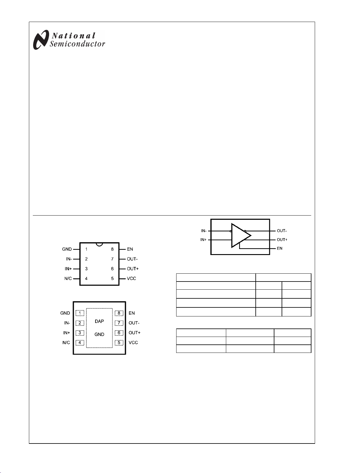
Connection and Block Diagrams
SOIC - Top View
20024705
LLP - Top View
20024743
20024702
Functional Operation
BLVDS Inputs BLVDS Outputs
[IN+] − [IN−] OUT+ OUT−
VID ≥ 0.1V
VID ≤ −0.1V
−0.1V ≤ VID ≤ 0.1V
H L
L H
Undefined Undefined
Ordering Information
Order Number NS Pkg. No. Pkg. Type
DS92001TMA M08A SOIC
DS92001TLD LDA08A LLP
© 2008 National Semiconductor Corporation 200247 www.national.com
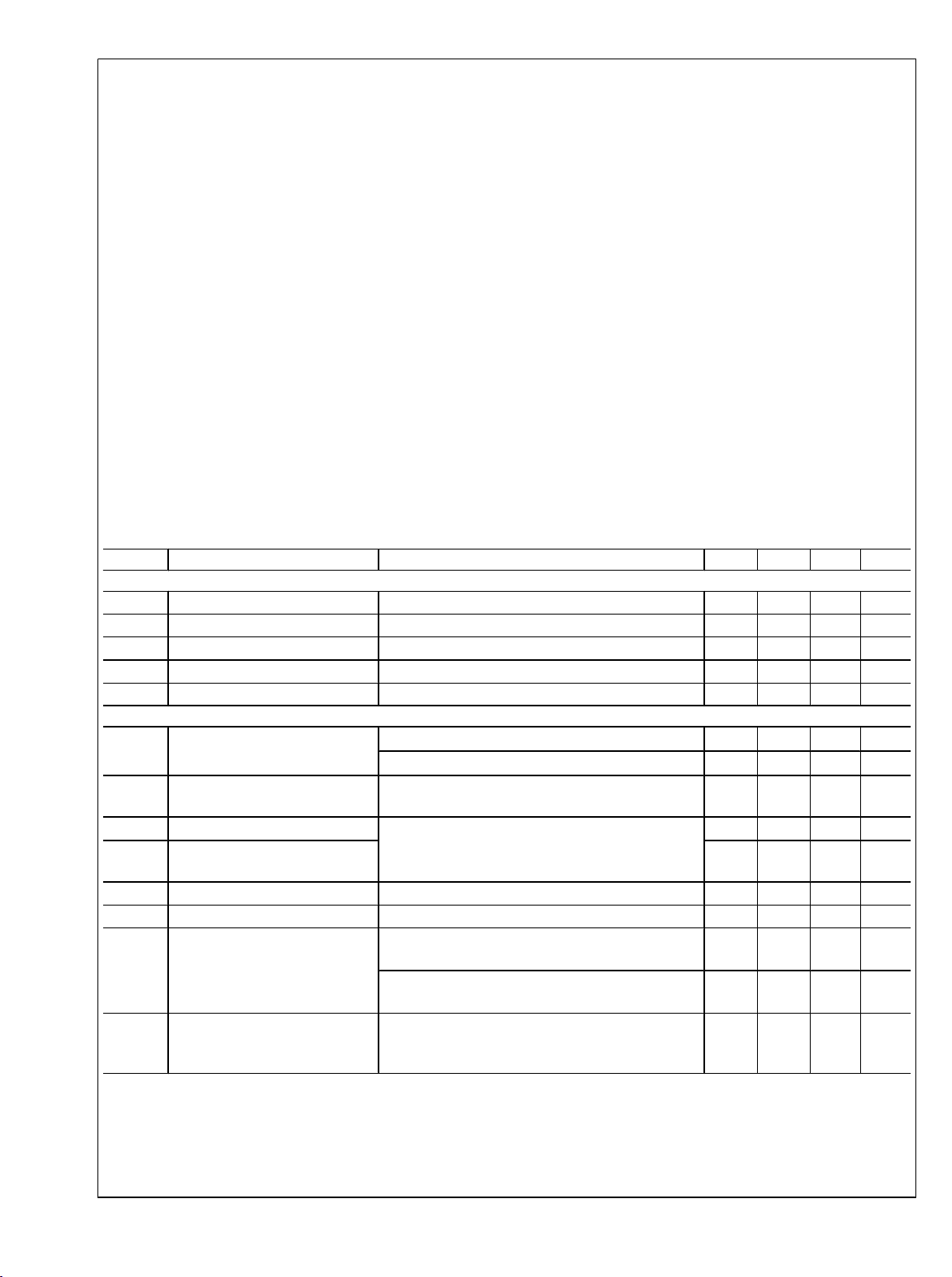
Absolute Maximum Ratings (Note 1)
If Military/Aerospace specified devices are required,
DS92001
please contact the National Semiconductor Sales Office/
Distributors for availability and specifications.
Supply Voltage (VCC)
LVCMOS/LVTTL Input Voltage
(EN)
B/LVDS Receiver Input Voltage
−0.3V to (VCC + 0.3V)
−0.3V to +4V
Maximum Package Power Dissipation at 25°C
M Package 726 mW
Derate M Package 5.8 mW/°C above +25°C
LDA Package 2.44 W
Derate LDA Package 19.49 mW/°C above +25°C
ESD Ratings
(HBM, 1.5kΩ, 100pF)
(EIAJ, 0Ω, 200pF)
(IN+, IN−) −0.3V to +4V
BLVDS Driver Output Voltage
(OUT+, OUT−) −0.3V to +4V
BLVDS Output Short Circuit
Current
Continuous
Junction Temperature +150°C
Storage Temperature Range −65°C to +150°C
Lead Temperature Range
Soldering (4 sec.) +260°C
Recommended Operating Conditions
Min Typ Max Units
Supply Voltage (VCC) 3.0 3.3 3.6 V
Receiver Differential Input
Voltage (VID) with
VCM=1.2V
Operating Free Air
Temperature
B/LVDS Input Rise/Fall
20% to 80%
0.1 2.4 |V|
−40 +25 +85 °C
2 20 ns
Electrical Characteristics
Over recommended operating supply and temperature ranges unless otherwise specified. (Notes 2, 3)
Symbol Parameter Conditions Min Typ Max Units
LVCMOS/LVTTL DC SPECIFICATIONS (EN)
V
IH
V
IL
I
IH
I
IL
V
CL
BLVDS OUTPUT DC SPECIFICATIONS (OUT)
|VOD| Differential Output Voltage (Note
ΔV
V
OS
ΔV
I
OZ
I
OFF
I
OS1
I
OSD
High Level Input Voltage 2.0 V
Low Level Input Voltage GND 0.8 V
High Level Input Current VIN = VCC or 2.0V +7 +20
Low Level Input Current VIN = GND or 0.8V −10 ±1 +10
Input Clamp Voltage ICL = −18 mA −0.6 −1.5 V
RL = 27Ω
2)
Change in Magnitude of VOD for
OD
RL = 50Ω
RL = 27Ω or 50Ω Figure 1, Figure 2
Complimentary Output States
Offset Voltage
Change in Magnitude of VOS for
OS
RL = 27Ω or RL = 50Ω
Figure 1
Complimentary Output States
Output TRI-STATE Current EN = 0V, V
= VCC or GND −20
OUT
Power-Off Leakage Current VCC = 0V or Open Circuit, V
Output Short Circuit Current (Note4)EN = VCC, VCM = 1.2V,VID = 200mV, V
VID = −200mV, VCM = 1.2V, V
VID = −200mV, VCM = 1.2V, V
VID = 200mV, VCM =1.2V, V
Differential Output Short Circuit
Current (Note 4)
EN = VCC, VID = |200mV|, VCM. = 1.2V, VOD = 0V
(connect true and complement outputs through a
= 3.6V −20
OUT
= 0V, or
OUT+
= 0V
OUT−
= VCC , or
OUT+
= V
OUT−
CC
250 350 500 mV
350 450 600 mV
20 mV
1.1 1.25 1.375 V
2 20 mV
±5 +20
±5 +20
−30 −60 mA
53 80 mA
|30| |42| mA
current meter)
CC
≥2.5kV
≥250V
V
μA
μA
μA
μA
www.national.com 2
Symbol Parameter Conditions Min Typ Max Units
B/LVDS RECEIVER DC SPECIFICATIONS (IN)
V
TH
Differential Input High Threshold
VCM = +0.05V, +1.2V or +3.25V −30 −5 mV
(Note 5)
V
TL
Differential Input Low Threshold
−70 −30 mV
(Note 5)
V
CMR
Common Mode Voltage Range
(Note 5)
|VID|/2 V
CC
V
−|VID|/
2
I
ΔI
IN
IN
Input Current VIN = V
VIN = 0V |1.5| |20|
Change in Magnitude of I
IN
VIN = V
VIN = 0V 1 6
CC
CC
VCC = 3.6V or 0V |1.5| |20|
1 6
μA
μA
μA
μA
SUPPLY CURRENT
I
CCD
Total Dynamic Supply Current
(includes load current)
EN = VCC, RL = 27Ω or 50Ω, CL = 15 pF,
Freq. = 200MHz 50% duty cycle,
50 65 mA
VID = 200mV, VCM = 1.2V
I
CCZ
TRI-STATE Supply Current EN = 0V,Freq. = 200MHz 50% duty cycle,
36 46 mA
VID = 200mV, VCM= 1.2V
DS92001
3 www.national.com
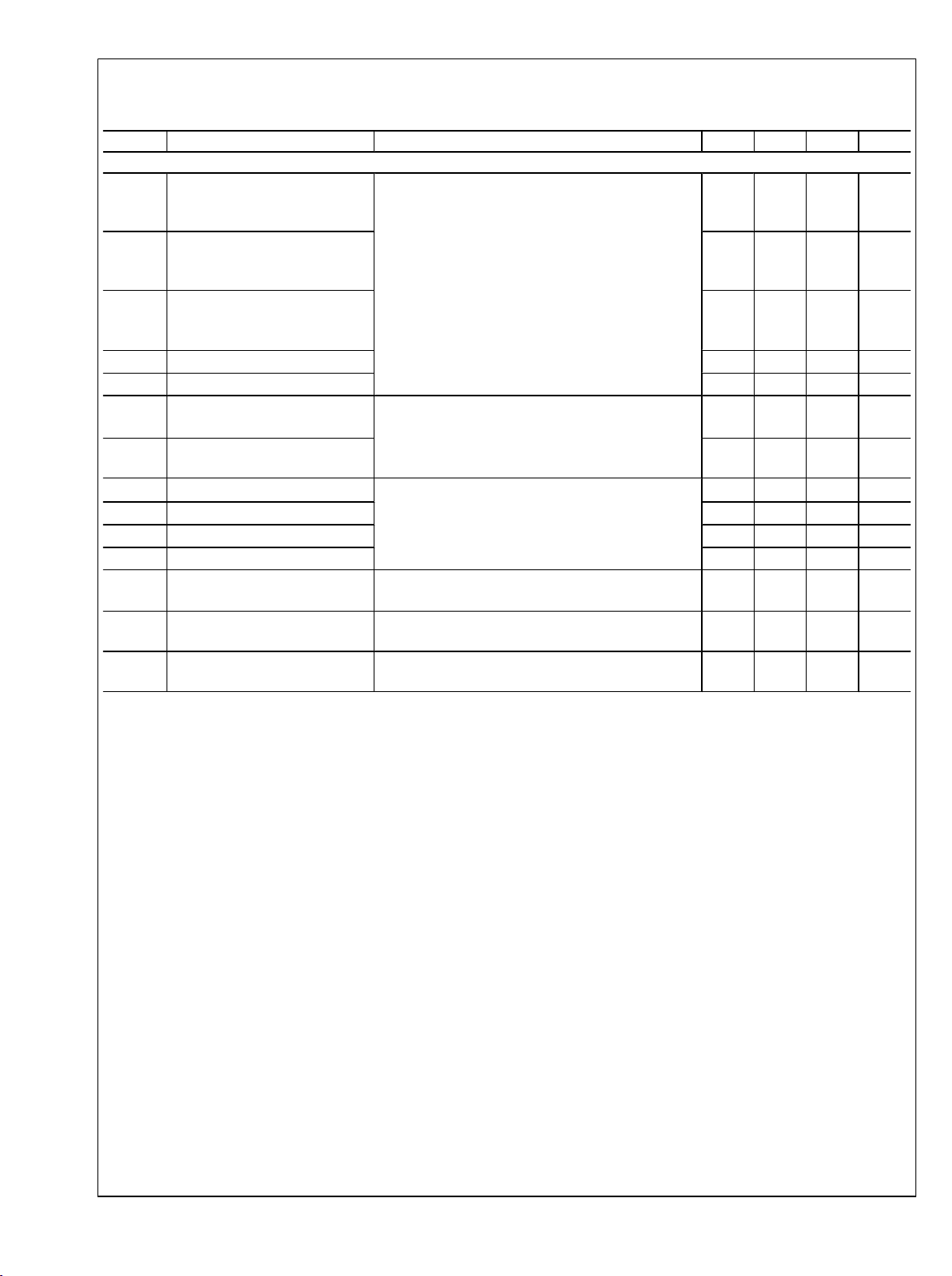
AC Electrical Characteristics
Over recommended operating supply and temperature ranges unless otherwise specified. (Note 3)
DS92001
Symbol Parameter Conditions Min Typ Max Units
LVDS OUTPUT AC SPECIFICATIONS (OUT)
t
PHLD
t
PLHD
t
SKD1
t
SKD3
t
SKD4
t
LHT
t
HLT
t
PHZ
t
PLZ
t
PZH
t
PZL
t
DJ
t
RJ
Differential Propagation Delay
High to Low
(Note 10)
Differential Propagation Delay
VID = 200mV, VCM = 1.2V,
RL = 27Ω or 50Ω, CL = 15pF
Figure 3 and Figure 4
1.0 1.4 2.0 ns
1.0 1.4 2.0 ns
Low to High
(Note 10)
Pulse Skew |t
PLHD
− t
PHLD
|
0 20 200 ps
(measure of duty cycle)
(Notes 5, 6)
Part-to-Part Skew (Notes 5, 7) 0 200 300 ps
Part-to-Part Skew (Notes 5, 8) 0 1 ns
Rise Time (Notes 5, 10)
20% to 80% points
Fall Time (Notes 5, 10)
RL = 50Ω or 27Ω, CL = 15pF
Figure 3 and Figure 5
0.350 0.6 1.0 ns
0.350 0.6 1.0 ns
80% to 20% points
Disable Time (Active High to Z)
Disable Time (Active Low to Z)
RL = 50Ω, CL = 15pF
Figure 6 and Figure 7
3 25 ns
3 25 ns
Enable Time (Z to Active High) 100 120 ns
Enable Time (Z to Active Low) 100 120 ns
LVDS Data Jitter, Deterministic
(Peak-to-Peak) (Note 9)
LVDS Clock Jitter, Random (Note9)VID = 300mV; VCM = 1.2V at 200MHz clock
VID = 300mV; PRBS = 223 − 1 data; VCM = 1.2V at
400Mbps (NRZ)
78 ps
36 ps
f
MAX
Note 1: “Absolute Maximum Ratings” are those values beyond which the safety of the device cannot be guaranteed. They are not meant to imply that the device
should be operated at these limits. The table of “Electrical Characteristics” specifies conditions of device operation.
Note 2: Current into device pins is defined as positive. Current out of device pins is defined as negative. All voltages are referenced to ground except VID, VOD,
VTH, VTL, and ΔVOD. VOD has a value and direction. Positive direction means OUT+ is a more positive voltage than OUT−.
Note 3: All typical are given for VCC = +3.3V and TA = +25°C, unless otherwise stated.
Note 4: Output short circuit current (IOS) is specified as magnitude only, minus sign indicates direction only.
Note 5: The parameters are guaranteed by design. The limits are based on statistical analysis of the device performance over the PVT (process, voltage and
temperature) range.
Note 6: t
the same channel (a measure of duty cycle).
Note 7: t
applies to devices at the same VCC and within 5°C of each other within the operating temperature range. This parameter guaranteed by design and characterization.
Note 8: t
operating temperature and voltage ranges, and across process distribution. t
Note 9: The parameters are guaranteed by design. The limits are based on statistical analysis of the device performance over the PVT range with the following
test equipment setup: Agilent 86130A used as stimulus, 5 feet of RG142B cable with DUT test board and Agilent 86100A (digital scope mainframe) with Agilent
86122A (20GHz scope module). Data input jitter pk to pk = 22 picoseconds; Clock input jitter = 24 picoseconds; tDJ measured 100 picoseconds, tRJ measured
60 picoseconds.
Note 10: Propagation delay, rise and fall times are guaranteed by design and characterization to 200MHz. Generator for these tests: 50MHz ≤ f ≤ 200MHz, Zo
= 50Ω, tr, tf ≤ 0.5ns. Generator used was HP8130A (300MHz capability).
Note 11: f
is guaranteed by design and characterization. A minimum is specified, which means that the device will operate to specified conditions from DC to the minimum
guaranteed AC frequency. The typical value is always greater than the minimum guarantee.
Maximum guaranteed frequency
(Note 11)
, |t
− t
SKD1
PLHD
, Part to Part Skew, is defined as the difference between the minimum and maximum specified differential propagation delays. This specification
SKD3
, Part to Part Skew, is the differential channel-to- channel skew of any event between devices. This specification applies to devices over recommended
SKD4
test: Generator (HP8133A or equivalent), Input duty cycle = 50%. Output criteria: VOD ≥ 200mV, Duty Cycle better than 45/55%. This specification
MAX
|, is the magnitude difference in differential propagation delay time between the positive going edge and the negative going edge of
PHLD
VID = 200mV, VCM = 1.2V
is defined as |Max − Min| differential propagation delay.
SKD4
200 300 MHz
www.national.com 4
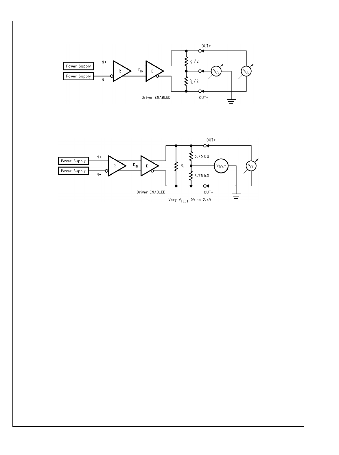
DC Test Circuits
DS92001
20024703
FIGURE 1. Differential Driver DC Test Circuit
FIGURE 2. Differential Driver Full Load DC Test Circuit
20024708
5 www.national.com
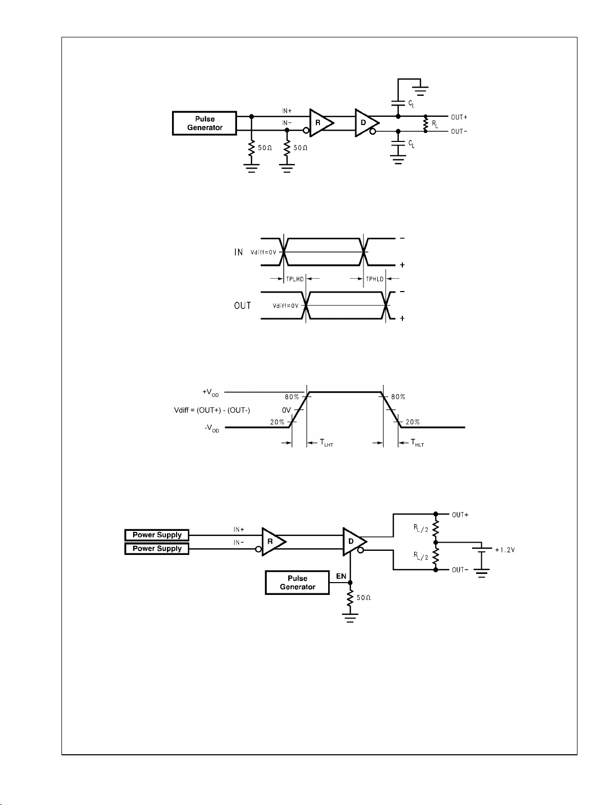
AC Test Circuits and Timing Diagrams
DS92001
FIGURE 3. BLVDS Output Load
FIGURE 4. Propagation Delay Low-to-High and High-to-Low
20024706
20024707
FIGURE 5. BLVDS Output Transition Time
FIGURE 6. TRI-STATE Delay Test Circuit
20024709
20024701
www.national.com 6
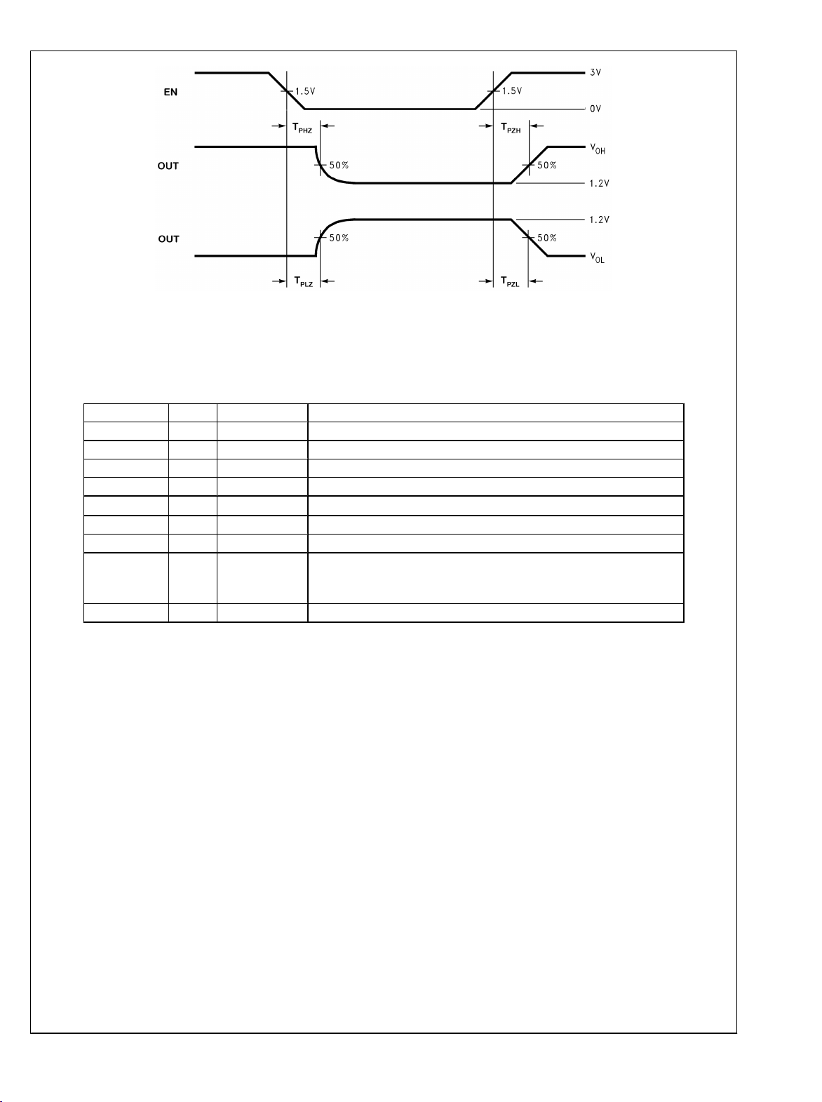
FIGURE 7. Output active to TRI-STATE and TRI-STATE to active output time
Pin Descriptions (SOIC and LLP)
Pin Name Pin # Input/Output Description
GND 1 P Ground
IN − 2 I Inverting receiver B/LVDS input pin
IN+ 3 I Non-inverting receiver B/LVDS input pin
N/C 4 NA "NO CONNECT" pin
V
CC
OUT+ 6 O Non-inverting driver BLVDS output pin
OUT - 7 O Inverting driver BLVDS output pin
EN 8 I Enable pin. When EN is LOW, the driver is disabled and the BLVDS
GND DAP P LLP Package Ground
5 P Power Supply, 3.3V ± 0.3V.
outputs are in TRI-STATE. When EN is HIGH, the driver is enabled.
LVCMOS/LVTTL levels.
DS92001
20024704
7 www.national.com
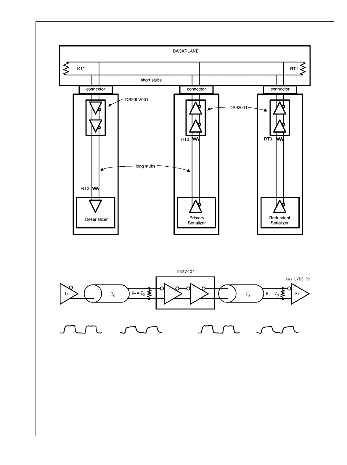
Typical Applications
DS92001
FIGURE 8. Backplane Stub-Hider Application
FIGURE 9. Cable Repeater Application
20024711
20024710
www.national.com 8

Application Information
The DS92001 can be used as a "stub-hider." In many systems, signals are distributed across backplanes, and one of
the limiting factors for system speed is the "stub length" or the
distance between the transmission line and the unterminated
receivers on the individual cards. See Figure 8. Although it is
generally recognized that this distance should be as short as
possible to maximize system performance, real-world packaging concerns and PCB designs often make it difficult to
make the stubs as short as the designer would like. The
DS92001, available in the LLP (Leadless Leadframe Package) package, can improve system performance by allowing
the receiver to be placed very close to the main transmission
line either on the backplane itself or very close to the connector on the card. Longer traces to the LVDS receiver may
be placed after the DS92001. This very small LLP package is
a 75% space savings over the SOIC package.
The DS92001 may also be used as a repeater as shown in
Figure 9. The signal is recovered and redriven at full strength
down the following segment. The DS92001 may also be used
as a level translator, as it accepts LVDS, BLVDS, and
LVPECL inputs.
POWER DECOUPLING RECOMMENDATIONS
Bypass capacitors must be used on power pins. Use high frequency ceramic (surface mount is recommended) 0.1μF and
0.01μF capacitors in parallel at the power supply pin with the
smallest value capacitor closest to the device supply pin. Additional scattered capacitors over the printed circuit board will
improve decoupling. Multiple vias should be used to connect
the decoupling capacitors to the power planes. A 10μF (35V)
or greater solid tantalum capacitor should be connected at the
power entry point on the printed circuit board between the
supply and ground.
PC BOARD CONSIDERATIONS
Use at least 4 PCB board layers (top to bottom): LVDS signals, ground, power, TTL signals.
Isolate TTL signals from LVDS signals, otherwise the TTL
signals may couple onto the LVDS lines. It is best to put TTL
and LVDS signals on different layers which are isolated by a
power/ground plane(s).
Keep drivers and receivers as close to the (LVDS port side)
connectors as possible.
For PC board considerations for the LLP package, please refer to application note AN-1187 “Leadless Leadframe Package.” It is important to note that to optimize signal integrity
(minimize jitter and noise coupling), the LLP thermal land pad,
which is a metal (normally copper) rectangular region located
under the package as seen in Figure 10, should be attached
to ground and match the dimensions of the exposed pad on
the PCB (1:1 ratio).
DS92001
20024744
FIGURE 10. LLP Thermal Land Pad and Pin Pads - Top
View
DIFFERENTIAL TRACES
Use controlled impedance traces which match the differential
impedance of your transmission medium (ie. cable) and termination resistor. Run the differential pair trace lines as close
together as possible as soon as they leave the IC (stubs
should be < 10mm long). This will help eliminate reflections
and ensure noise is coupled as common-mode. In fact, we
have seen that differential signals which are 1mm apart radiate far less noise than traces 3mm apart since magnetic field
cancellation is much better with the closer traces. In addition,
noise induced on the differential lines is much more likely to
appear as common-mode which is rejected by the receiver.
Match electrical lengths between traces to reduce skew.
Skew between the signals of a pair means a phase difference
between signals which destroys the magnetic field cancellation benefits of differential signals and EMI will result. Do not
rely solely on the auto-route function for differential traces.
Carefully review dimensions to match differential impedance
and provide isolation for the differential lines. Minimize the
number of vias and other discontinuities on the line.
Avoid 90° turns (these cause impedance discontinuities). Use
arcs or 45° bevels.
Within a pair of traces, the distance between the two traces
should be minimized to maintain common-mode rejection of
the receivers. On the printed circuit board, this distance
should remain constant to avoid discontinuities in differential
impedance. Minor violations at connection points are allowable.
TERMINATION
Use a termination resistor which best matches the differential
impedance or your transmission line. The resistor should be
between 90Ω and 130Ω for point-to-point links. Multidrop
(driver in the middle) or multipoint configurations are typically
terminated at both ends. The termination value may be lower
than 100Ω due to loading effects and in the 50Ω to 100Ω
range. Remember that the current mode outputs need the
termination resistor to generate the differential voltage.
Surface mount 1% - 2% resistors are the best. PCB stubs,
component lead, and the distance from the termination to the
receiver inputs should be minimized. The distance between
the termination resistor and the receiver should be < 10mm
(12mm MAX).
PROBING LVDS TRANSMISSION LINES
Always use high impedance (> 100kΩ), low capacitance
(< 2 pF) scope probes with a wide bandwidth (1 GHz) scope.
Improper probing will give deceiving results.
9 www.national.com

Physical Dimensions inches (millimeters) unless otherwise noted
DS92001
Order Number DS92001TMA
See NS Package Number M08A
Order Number DS92001TLD
See NS Package Number LDA08A
www.national.com 10

Notes
DS92001
11 www.national.com

Notes
For more National Semiconductor product information and proven design tools, visit the following Web sites at:
Products Design Support
Amplifiers www.national.com/amplifiers WEBENCH www.national.com/webench
Audio www.national.com/audio Analog University www.national.com/AU
Clock Conditioners www.national.com/timing App Notes www.national.com/appnotes
Data Converters www.national.com/adc Distributors www.national.com/contacts
Displays www.national.com/displays Green Compliance www.national.com/quality/green
Ethernet www.national.com/ethernet Packaging www.national.com/packaging
Interface www.national.com/interface Quality and Reliability www.national.com/quality
LVDS www.national.com/lvds Reference Designs www.national.com/refdesigns
Power Management www.national.com/power Feedback www.national.com/feedback
Switching Regulators www.national.com/switchers
LDOs www.national.com/ldo
DS92001 3.3V B/LVDS-BLVDS Buffer
LED Lighting www.national.com/led
PowerWise www.national.com/powerwise
Serial Digital Interface (SDI) www.national.com/sdi
Temperature Sensors www.national.com/tempsensors
Wireless (PLL/VCO) www.national.com/wireless
THE CONTENTS OF THIS DOCUMENT ARE PROVIDED IN CONNECTION WITH NATIONAL SEMICONDUCTOR CORPORATION
(“NATIONAL”) PRODUCTS. NATIONAL MAKES NO REPRESENTATIONS OR WARRANTIES WITH RESPECT TO THE ACCURACY
OR COMPLETENESS OF THE CONTENTS OF THIS PUBLICATION AND RESERVES THE RIGHT TO MAKE CHANGES TO
SPECIFICATIONS AND PRODUCT DESCRIPTIONS AT ANY TIME WITHOUT NOTICE. NO LICENSE, WHETHER EXPRESS,
IMPLIED, ARISING BY ESTOPPEL OR OTHERWISE, TO ANY INTELLECTUAL PROPERTY RIGHTS IS GRANTED BY THIS
DOCUMENT.
TESTING AND OTHER QUALITY CONTROLS ARE USED TO THE EXTENT NATIONAL DEEMS NECESSARY TO SUPPORT
NATIONAL’S PRODUCT WARRANTY. EXCEPT WHERE MANDATED BY GOVERNMENT REQUIREMENTS, TESTING OF ALL
PARAMETERS OF EACH PRODUCT IS NOT NECESSARILY PERFORMED. NATIONAL ASSUMES NO LIABILITY FOR
APPLICATIONS ASSISTANCE OR BUYER PRODUCT DESIGN. BUYERS ARE RESPONSIBLE FOR THEIR PRODUCTS AND
APPLICATIONS USING NATIONAL COMPONENTS. PRIOR TO USING OR DISTRIBUTING ANY PRODUCTS THAT INCLUDE
NATIONAL COMPONENTS, BUYERS SHOULD PROVIDE ADEQUATE DESIGN, TESTING AND OPERATING SAFEGUARDS.
EXCEPT AS PROVIDED IN NATIONAL’S TERMS AND CONDITIONS OF SALE FOR SUCH PRODUCTS, NATIONAL ASSUMES NO
LIABILITY WHATSOEVER, AND NATIONAL DISCLAIMS ANY EXPRESS OR IMPLIED WARRANTY RELATING TO THE SALE
AND/OR USE OF NATIONAL PRODUCTS INCLUDING LIABILITY OR WARRANTIES RELATING TO FITNESS FOR A PARTICULAR
PURPOSE, MERCHANTABILITY, OR INFRINGEMENT OF ANY PATENT, COPYRIGHT OR OTHER INTELLECTUAL PROPERTY
RIGHT.
LIFE SUPPORT POLICY
NATIONAL’S PRODUCTS ARE NOT AUTHORIZED FOR USE AS CRITICAL COMPONENTS IN LIFE SUPPORT DEVICES OR
SYSTEMS WITHOUT THE EXPRESS PRIOR WRITTEN APPROVAL OF THE CHIEF EXECUTIVE OFFICER AND GENERAL
COUNSEL OF NATIONAL SEMICONDUCTOR CORPORATION. As used herein:
Life support devices or systems are devices which (a) are intended for surgical implant into the body, or (b) support or sustain life and
whose failure to perform when properly used in accordance with instructions for use provided in the labeling can be reasonably expected
to result in a significant injury to the user. A critical component is any component in a life support device or system whose failure to perform
can be reasonably expected to cause the failure of the life support device or system or to affect its safety or effectiveness.
National Semiconductor and the National Semiconductor logo are registered trademarks of National Semiconductor Corporation. All other
brand or product names may be trademarks or registered trademarks of their respective holders.
Copyright© 2008 National Semiconductor Corporation
For the most current product information visit us at www.national.com
www.national.com
National Semiconductor
Americas Technical
Support Center
Email: support@nsc.com
Tel: 1-800-272-9959
National Semiconductor Europe
Technical Support Center
Email: europe.support@nsc.com
German Tel: +49 (0) 180 5010 771
English Tel: +44 (0) 870 850 4288
National Semiconductor Asia
Pacific Technical Support Center
Email: ap.support@nsc.com
National Semiconductor Japan
Technical Support Center
Email: jpn.feedback@nsc.com
 Loading...