

DS91M040
125 MHz Quad M-LVDS Transceiver
DS91M040 125 MHz Quad M-LVDS Transceiver
May 13, 2008
General Description
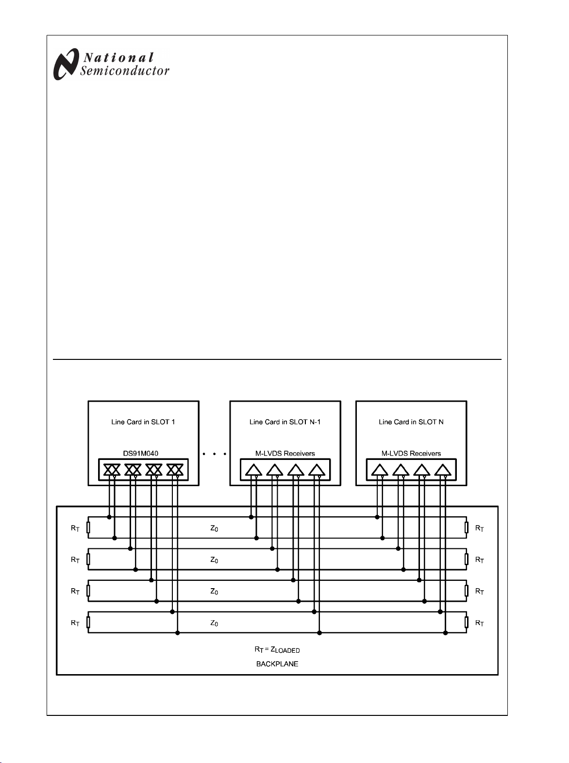
The DS91M040 is a quad M-LVDS transceiver designed for
driving / receiving clock or data signals to / from up to four
multipoint networks.
M-LVDS (Multipoint LVDS) is a new family of bus interface
devices based on LVDS technology specifically designed for
multipoint and multidrop cable and backplane applications. It
differs from standard LVDS in providing increased drive current to handle double terminations that are required in multipoint applications. Controlled transition times minimize reflections that are common in multipoint configurations due to
unterminated stubs. M-LVDS devices also have a very large
input common mode voltage range for additional noise margin
in heavily loaded and noisy backplane environments.
A single DS91M040 channel is a half-duplex transceiver that
accepts LVTTL/LVCMOS signals at the driver inputs and converts them to differential M-LVDS signal levels. The receiver
inputs accept low voltage differential signals (LVDS, BLVDS,
M-LVDS, LVPECL and CML) and convert them to 3V LVCMOS signals. The DS91M040 supports both M-LVDS type 1
and type 2 receiver inputs.
Typical Application
Features
DC - 125 MHz / 250 Mbps low jitter, low skew, low power
■
operation
Wide Input Common Mode Voltage Range allows up to
■
±2V of GND noise
Conforms to TIA/EIA-899 M-LVDS Standard
■
Pin selectable M-LVDS receiver type (1 or 2)
■
Controlled transition times (2.0 ns typ) minimize reflections
■
8 kV ESD on M-LVDS I/O pins protects adjoining
■
components
Flow-through pinout simplifies PCB layout
■
Small 5 mm x 5 mm LLP-32 space saving package
■
Applications
Multidrop / Multipoint clock and data distribution
■
High-Speed, Low Power, Short-Reach alternative to TIA/
■
EIA-485/422
Clock distribution in AdvancedTCA (ATCA) and
■
MicroTCA (μTCA) backplanes
30042202
© 2008 National Semiconductor Corporation 300422 www.national.com
Ordering Information
Order Number Receiver Input Function Package Type
DS91M040
DS91M040TSQ Type 1 or 2 Quad M-LVDS Transciever LLP-32
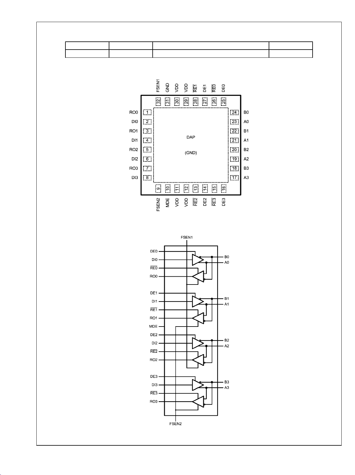
Connection Diagram
Logic Diagram
30042201
www.national.com 2
30042203
Pin Descriptions
Number Name I/O, Type Description
1, 3, 5, 7 RO O, LVCMOS Receiver output pin.
26, 28, 13, 15 RE I, LVCMOS Receiver enable pin: When RE is high, the receiver is disabled.
25, 27, 14, 16 DE I, LVCMOS Driver enable pin: When DE is low, the driver is disabled. When
2, 4, 6, 8 DI I, LVCMOS Driver input pin.
31, DAP GND Power Ground pin and pad.
17, 19, 21, 23 A I/O, M-LVDS Non-inverting driver output pin/Non-inverting receiver input pin
18, 20, 22, 24 B I/O, M-LVDS Inverting driver output pin/Inverting receiver input pin
11, 12, 29, 30 V
32 FSEN1 I, LVCMOS
9 FSEN2 I, LVCMOS
10 MDE I, LVCMOS Master enable pin. When MDE is H, the device is powered up.
DD
DS91M040
When RE is low, the receiver is enabled. There is a 300 kΩ pullup
resistor on this pin.
DE is high, the driver is enabled. There is a 300 kΩ pulldown
resistor on this pin.
Power Power supply pin, +3.3V ± 0.3V
Failsafe enable pin with a 300 kΩ pullup resistor. This pin
enables Type 2 receiver on inputs 0 and 2.
FSEN1 = L --> Type 1 receiver inputs
FSEN1 = H --> Type 2 receiver inputs
Failsafe enable pin with a 300 kΩ pullup resistor. This pin
enables Type 2 receiver on inputs 1 and 3.
FSEN2 = L --> Type 1 receiver inputs
FSEN2 = H --> Type 2 receiver inputs
When MDE is L, the device overrides all other control and powers
down.
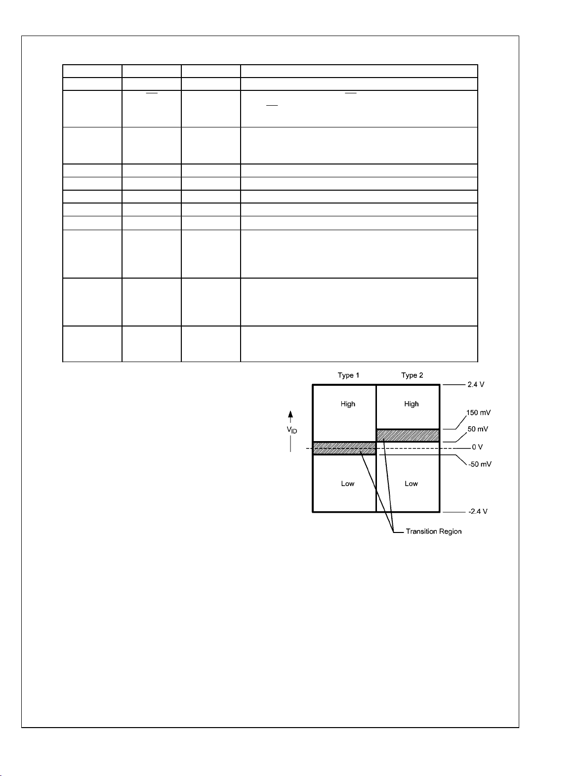
M-LVDS Receiver Types
The EIA/TIA-899 M-LVDS standard specifies two different
types of receiver input stages. A type 1 receiver has a conventional threshold that is centered at the midpoint of the input
amplitude, VID/2. A type 2 receiver has a built in offset that is
100mV greater then VID/2. The type 2 receiver offset acts as
a failsafe circuit where open or short circuits at the input will
always result in the output stage being driven to a low logic
state.
30042240
FIGURE 1. M-LVDS Receiver Input Thresholds
3 www.national.com
Absolute Maximum Ratings (Note 4)
If Military/Aerospace specified devices are required,
please contact the National Semiconductor Sales Office/
DS91M040
Distributors for availability and specifications.
Power Supply Voltage −0.3V to +4V
LVCMOS Input Voltage −0.3V to (VDD + 0.3V)
LVCMOS Output Voltage −0.3V to (VDD + 0.3V)
M-LVDS I/O Voltage −5.5V to +5.5V
M-LVDS Output Short Circuit
ESD Susceptibility
HBM (Note 1)
MM (Note 2)
CDM (Note 3)
Note 1: Human Body Model, applicable std. JESD22-A114C
Note 2: Machine Model, applicable std. JESD22-A115-A
Note 3: Field Induced Charge Device Model, applicable std.
JESD22-C101-C
Current Duration Continuous
Junction Temperature +140°C
Storage Temperature Range −65°C to +150°C
Lead Temperature Range
Soldering (4 sec.) +260°C
Maximum Package Power Dissipation @ +25°C
SQ Package 833 mW
Derate SQ Package 6.67 mW/°C above +25°C
Package Thermal Resistance
θ
θ
JA
JC
+150°C/W
+63.8°C/W
Recommended Operating Conditions
Min Typ Max Units
Supply Voltage, V
DD
Voltage at Any Bus Terminal −1.4 +3.8 V
(Separate or Common-Mode)
Differential Input Voltage V
LVTTL Input Voltage High V
LVTTL Input Voltage Low V
Operating Free Air
Temperature T
A
3.0 3.3 3.6 V
ID
2.4 V
2.0 V
IH
0 0.8 V
IL
−40 +25 +85 °C
DD
DC Electrical Characteristics (Notes 5, 6, 7, 9)
Over recommended operating supply and temperature ranges unless otherwise specified.
Symbol Parameter Conditions Min Typ Max Units
M-LVDS Driver
|VAB| Differential output voltage magnitude
ΔV
AB
Change in differential output voltage magnitude
between logic states
V
OS(SS)
|ΔV
OS(SS)
Steady-state common-mode output voltage
Change in steady-state common-mode output
|
voltage between logic states
V
V
V
A(OC)
B(OC)
P(H)
Maximum steady-state open-circuit output voltage Figure 5 0 2.4 V
Maximum steady-state open-circuit output voltage
Voltage overshoot, low-to-high level output
(Note 12)
V
P(L)
Voltage overshoot, high-to-low level output
(Note 12)
I
IH
I
IL
V
CL
I
OS
High-level input current (LVTTL inputs) VIH = 2.0V -15 15
Low-level input current (LVTTL inputs) VIL = 0.8V -15 15
Input Clamp Voltage (LVTTL inputs) IIN = -18 mA -1.5 V
Differential short-circuit output current (Note 8) Figure 6 -43 43 mA
M-LVDS Receiver
V
V
V
V
I
OZ
I
OSR
IT+
IT−
OH
OL
Positive-going differential input voltage threshold See Function Tables Type 1 16 50 mV
Negative-going differential input voltage threshold See Function Tables Type 1 −50 20 mV
High-level output voltage (LVTTL output) IOH = −8mA 2.4 2.7
Low-level output voltage (LVTTL output) IOL = 8mA 0.28
TRI-STATE output current VO = 0V or 3.6V −10 10
Short-circuit receiver output current (LVTTL output) VO = 0V -50 -90 mA
RL = 50Ω, CL = 5 pF
Figures 2, 4
RL = 50Ω, CL = 5 pF
Figures 2, 3
RL = 50Ω, CL = 5pF, CD = 0.5 pF
Figures 7, 8
Type 2 100 150 mV
Type 2 50 94 mV
480 650 mV
−50 0 +50 mV
0.3 1.6 2.1 V
0 +50 mV
0 2.4 V
−0.2V
S
S
1.2V
V
0.4 V
≥8 kV
≥250V
≥1250V
V
SS
V
V
μA
μA
μA
www.national.com 4
Symbol Parameter Conditions Min Typ Max Units
M-LVDS Bus (Input and Output) Pins
I
A
Transceiver input/output current VA = 3.8V, VB = 1.2V 32 µA
VA = 0V or 2.4V, VB = 1.2V −20 +20 µA
VA = −1.4V, VB = 1.2V −32 µA
I
B
Transceiver input/output current VB = 3.8V, VA = 1.2V 32 µA
VB = 0V or 2.4V, VA = 1.2V −20 +20 µA
VB = −1.4V, VA = 1.2V −32 µA
I
AB
I
A(OFF)
I
B(OFF)
I
AB(OFF)
C
A
C
B
C
AB
C
A/B
Transceiver input/output differential current (IA − IB)
VA = VB, −1.4V ≤ V ≤ 3.8V
Transceiver input/output power-off current VA = 3.8V, VB = 1.2V,
DE = VCC = 1.5V
VA = 0V or 2.4V, VB = 1.2V,
DE = VCC = 1.5V
VA = −1.4V, VB = 1.2V,
DE = VCC = 1.5V
Transceiver input/output power-off current VB = 3.8V, VA = 1.2V,
DE = VCC = 1.5V
VB = 0V or 2.4V, VA = 1.2V,
DE = VCC = 1.5V
VB = −1.4V, VA = 1.2V,
DE = VCC = 1.5V
Transceiver input/output power-off differential
current (I
A(OFF)
− I
B(OFF)
)
VA = VB, −1.4V ≤ V ≤ 3.8V,
VDD = 1.5V, DE = 1.5V
−4 +4 µA
32 µA
−20 +20 µA
−32 µA
32 µA
−20 +20 µA
−32 µA
−4 +4 µA
Transceiver input/output capacitance VDD = OPEN 7.8 pF
Transceiver input/output capacitance 7.8 pF
Transceiver input/output differential capacitance 3 pF
Transceiver input/output capacitance balance (CA/
CB)
1
SUPPLY CURRENT (VCC)
I
CCD
I
CCZ
I
CCR
I
CCPD
Driver Supply Current
RL = 50Ω, DE = H, RE = H
67 75 mA
TRI-STATE Supply Current DE = L, RE = H 22 26 mA
Receiver Supply Current DE = L, RE = L 32 38 mA
Power Down Supply Current MDE = L 3 5 mA
DS91M040
Note 4: “Absolute Maximum Ratings” indicate limits beyond which damage to the device may occur, including inoperability and degradation of device reliability
and/or performance. Functional operation of the device and/or non-degradation at the Absolute Maximum Ratings or other conditions beyond those indicated in
the Recommended Operating Conditions is not implied. The Recommended Operating Conditions indicate conditions at which the device is functional and the
device should not be operated beyond such conditions.
Note 5: The Electrical Characteristics tables list guaranteed specifications under the listed Recommended Operating Conditions except as otherwise modified
or specified by the Electrical Characteristics Conditions and/or Notes. Typical specifications are estimations only and are not guaranteed.
Note 6: Current into device pins is defined as positive. Current out of device pins is defined as negative. All voltages are referenced to ground except VOD and
ΔVOD.
Note 7: Typical values represent most likely parametric norms for VDD = +3.3V and TA = +25°C, and at the Recommended Operation Conditions at the time of
product characterization and are not guaranteed.
Note 8: Output short circuit current (IOS) is specified as magnitude only, minus sign indicates direction only.
Note 9: CL includes fixture capacitance and CD includes probe capacitance.
5 www.national.com
 Loading...