

Page 1
DS91D176/DS91C176
100 MHz Single Channel M-LVDS Transceivers
General Description
The DS91C176 and DS91D176 are 100 MHz single channel
M-LVDS (Multipoint Low Voltage Differential Signaling)
transceivers designed for applications that utilize multipoint
networks (e.g. clock distribution in ATCA and uTCA based
systems). M-LVDS is a new bus interface standard (TIA/
EIA-899) optimized for multidrop networks. Controlled edge
rates, tight input receiver thresholds and increased drive
strength are sone of the key enhancments that make M-LVDS
devices an ideal choice for distributing signals via multipoint
networks.
The DS91C176/DS91D176 are half-duplex transceivers that
accept LVTTL/LVCMOS signals at the driver inputs and convert them to differential M-LVDS signals. The receiver inputs
accept low voltage differential signals (LVDS, B-LVDS, MLVDS, LV-PECL and CML) and convert them to 3V LVCMOS
signals. The DS91D176 has a M-LVDS type 1 receiver input
with no offset. The DS91C176 has an M-LVDS type 2 receiver
which enable failsafe functionality.
Features
DC to 100+ MHz / 200+ Mbps low power, low EMI
■
operation
Optimal for ATCA, uTCA clock distribution networks
■
Meets or exceeds TIA/EIA-899 M-LVDS Standard
■
Wide Input Common Mode Voltage for Increased Noise
■
Immunity
DS91D176 has type 1 receiver input
■
DS91C176 has type 2 receiver with fail-safe
■
Industrial temperature range
■
Space saving SOIC-8 package
■
DS91D176/DS91C176 100 MHz Single Channel M-LVDS Transceivers
October 3, 2008
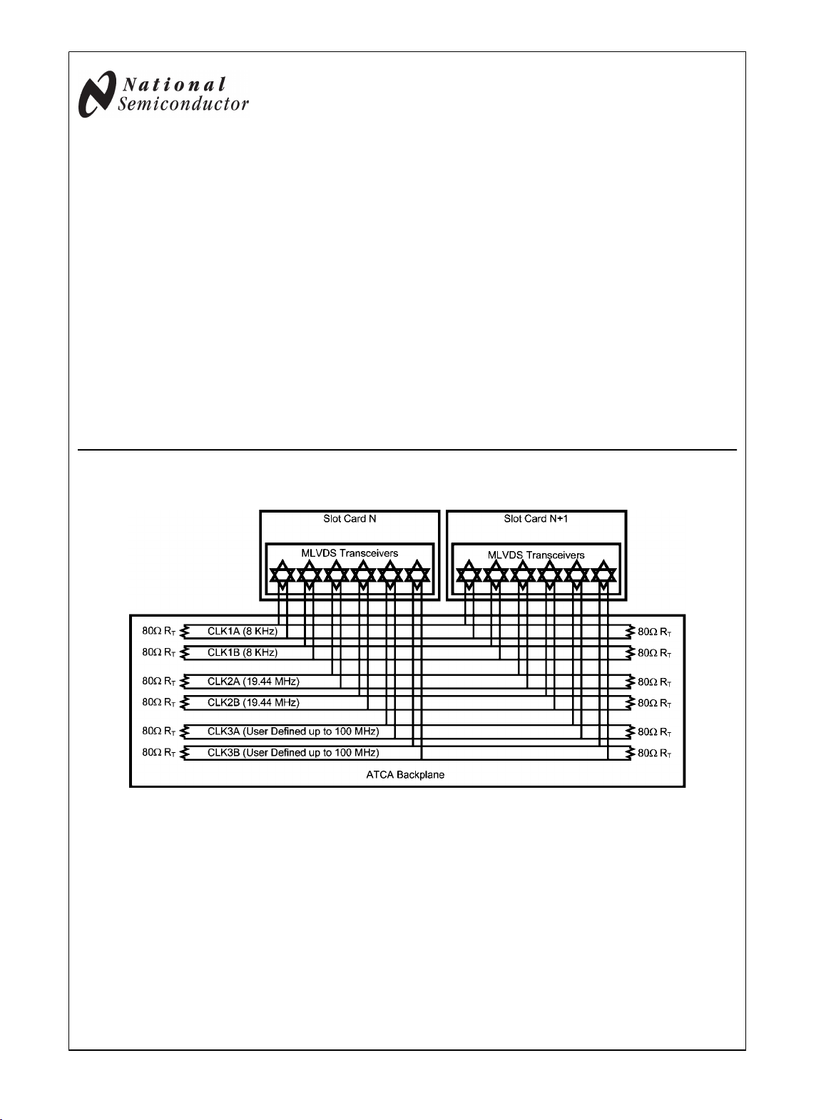
Typical Application in an ATCA Clock Distribution Network
20024630
© 2008 National Semiconductor Corporation 200246 www.national.com
Page 2
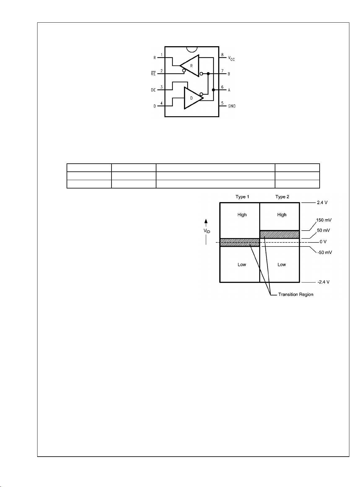
Connection and Logic Diagram
DS91D176/DS91C176
Order Number DS91D176TMA, DS91C176TMA
See NS Package Number M08A
Ordering Information
Order Number Receiver Input Function Package Type
DS91D176TMA type 1 Data (0V threshold receiver) SOIC/M08A
DS91C176TMA type 2 Control (100 mV offset fail-safe receiver) SOIC/M08A
M-LVDS Receiver Types
The EIA/TIA-899 M-LVDS standard specifies two different
types of receiver input stages. A type 1 receiver has a conventional threshold that is centered at the midpoint of the input
amplitude, VID/2. A type 2 receiver has a built in offset that is
100mV greater than VID/2. The type 2 receiver offset acts as
a failsafe circuit where open or short circuits at the input will
always result in the output stage being driven to a low logic
state.
Top View
20024601
www.national.com 2
20024640
FIGURE 1. M-LVDS Receiver Input Thresholds
Page 3
DS91D176/DS91C176
Absolute Maximum Ratings (Note 1)
If Military/Aerospace specified devices are required,
please contact the National Semiconductor Sales Office/
Distributors for availability and specifications.
Supply Voltage, V
CC
Control Input Voltages −0.3V to (VCC + 0.3V)
Driver Input Voltage −0.3V to (VCC + 0.3V)
Driver Output Voltages −1.8V to +4.1V
Receiver Input Voltages −1.8V to +4.1V
Receiver Output Voltage −0.3V to (VCC + 0.3V)
Maximum Package Power Dissipation at +25°C
SOIC Package 833 mW
Derate SOIC Package 6.67 mW/°C above +25°C
Thermal Resistance (4-Layer, 2 oz. Cu, JEDEC)
θ
JA
θ
JC
Maximum Junction Temperature 150°C
Storage Temperature Range −65°C to +150°C
−0.3V to +4V
150°C/W
63°C/W
Lead Temperature
(Soldering, 4 seconds) 260°C
ESD Ratings:
(HBM 1.5kΩ, 100pF) ≥ 8 kV
(EIAJ 0Ω, 200pF)
(CDM 0Ω, 0pF)
≥ 250 V
≥ 1000 V
Recommended Operating Conditions
Min Typ Max Units
Supply Voltage, V
CC
Voltage at Any Bus Terminal −1.4 +3.8 V
(Separate or Common-Mode)
Differential Input Voltage V
LVTTL Input Voltage High V
LVTTL Input Voltage Low V
Operating Free Air
Temperature T
A
3.0 3.3 3.6 V
ID
2.4 V
2.0 V
IH
0 0.8 V
IL
−40 +25 +85 °C
CC
V
Electrical Characteristics
Over recommended operating supply and temperature ranges unless otherwise specified. (Notes 2, 3, 4, 8)
Symbol Parameter Conditions Min Typ Max Units
M-LVDS Driver
|VAB| Differential output voltage magnitude
ΔV
AB
Change in differential output voltage magnitude
between logic states
V
OS(SS)
|ΔV
OS(SS)
Steady-state common-mode output voltage
Change in steady-state common-mode output
|
voltage between logic states
V
OS(PP)
V
A(OC)
V
B(OC)
V
P(H)
V
P(L)
I
IH
I
IL
V
IKL
I
OS
Peak-to-peak common-mode output voltage
Maximum steady-state open-circuit output voltage Figure 5 0 2.4 V
Maximum steady-state open-circuit output voltage
Voltage overshoot, low-to-high level output
Voltage overshoot, high-to-low level output −0.2V
High-level input current (LVTTL inputs) VIH = 2.0V -15 15
Low-level input current (LVTTL inputs) VIL = 0.8V -15 15
Input Clamp Voltage (LVTTL inputs) IIN = -18mA -1.5 V
Differential short-circuit output current Figure 6 -43 43 mA
M-LVDS Receiver
V
V
V
V
I
OZ
I
OSR
IT+
IT−
OH
OL
Positive-going differential input voltage threshold See Function Tables Type 1 20 50 mV
Negative-going differential input voltage threshold See Function Tables Type 1 −50 20 mV
High-level output voltage (LVTTL output) IOH = −8mA 2.4 2.7
Low-level output voltage (LVTTL output) IOL = 8mA 0.28
TRI-STATE output current VO = 0V or 3.6V −10 10
Short-circuit receiver output current (LVTTL output) VO = 0V -48 -90 mA
M-LVDS Bus (Input and Output) Pins
I
A
Transceiver input/output current VA = 3.8V, VB = 1.2V 32 µA
RL = 50Ω, CL = 5pF
Figure 2 and Figure 4
RL = 50Ω, CL = 5pF
Figure 2 and Figure 3
(V
@ 500KHz clock)
OS(PP)
RL = 50Ω, CL = 5pF, CD = 0.5pF
Figure 7 and Figure 8 (Note 9)
Type 2 94 150 mV
Type 2 50 94 mV
VA = 0V or 2.4V, VB = 1.2V −20 +20 µA
VA = −1.4V, VB = 1.2V −32 µA
480 650 mV
−50 0 +50 mV
0.3 1.8 2.1 V
0 +50 mV
135 mV
0 2.4 V
S
S
1.2V
SS
V
V
0.4 V
V
μA
μA
μA
3 www.national.com
Page 4
Symbol Parameter Conditions Min Typ Max Units
I
B
Transceiver input/output current VB = 3.8V, VA = 1.2V 32 µA
VB = 0V or 2.4V, VA = 1.2V −20 +20 µA
VB = −1.4V, VA = 1.2V −32 µA
I
AB
I
A(OFF)
DS91D176/DS91C176
Transceiver input/output differential current (IA − IB)
VA = VB, −1.4V ≤ V ≤ 3.8V
Transceiver input/output power-off current VA = 3.8V, VB = 1.2V,
DE = 0V
0V ≤ VCC ≤ 1.5V
−4 +4 µA
32 µA
VA = 0V or 2.4V, VB = 1.2V,
DE = 0V
−20 +20 µA
0V ≤ VCC ≤ 1.5V
VA = −1.4V, VB = 1.2V,
DE =0V
−32 µA
0V ≤ VCC ≤ 1.5V
I
B(OFF)
Transceiver input/output power-off current VB = 3.8V, VA = 1.2V,
DE = 0V
32 µA
0V ≤ VCC ≤ 1.5V
VB = 0V or 2.4V, VA = 1.2V,
DE = 0V
−20 +20 µA
0V ≤ VCC ≤ 1.5V
VB = −1.4V, VA = 1.2V,
DE = 0V
−32 µA
0V ≤ VCC ≤ 1.5V
I
AB(OFF)
Transceiver input/output power-off differential
current (I
A(OFF)
− I
B(OFF)
)
VA = VB, −1.4V ≤ V ≤ 3.8V,
DE = 0V
−4 +4 µA
0V ≤ VCC ≤ 1.5V
C
A
C
B
C
AB
C
A/B
Transceiver input/output capacitance VCC = OPEN 9 pF
Transceiver input/output capacitance 9 pF
Transceiver input/output differential capacitance 5.7 pF
Transceiver input/output capacitance balance
(CA/CB)
1.0
SUPPLY CURRENT (VCC)
I
CCD
I
CCZ
I
CCR
Driver Supply Current
RL = 50Ω, DE = VCC, RE = V
TRI-STATE Supply Current DE = GND, RE = V
CC
CC
20 29.5 mA
6 9.0 mA
Receiver Supply Current DE = GND, RE = GND 14 18.5 mA
www.national.com 4
Page 5
Switching Characteristics
Over recommended operating supply and temperature ranges unless otherwise specified. (Notes 3, 8)
Symbol Parameter Conditions Min Typ Max Units
DRIVER AC SPECIFICATION
t
PLH
t
PHL
t
(t
SKD1
sk(p)
t
SKD3
t
(tr) Rise Time (Note 9)
TLH
t
(tf) Fall Time (Note 9) 1.0 1.8 3.0 ns
THL
t
PZH
t
PZL
t
PLZ
t
PHZ
t
JIT
f
MAX
RECEIVER AC SPECIFICATION
t
PLH
t
PHL
t
(t
SKD1
sk(p)
t
SKD3
t
(tr) Rise Time (Note 9)
TLH
t
(tf) Fall Time (Note 9)
THL
t
PZH
t
PZL
t
PLZ
t
PHZ
f
MAX
Differential Propagation Delay Low to High
Differential Propagation Delay High to Low
) Pulse Skew |t
PLHD
− t
PHLD
| (Notes 5, 9)
Part-to-Part Skew (Notes 6, 9)
Enable Time (Z to Active High)
Enable Time (Z to Active Low )
Disable Time (Active Low to Z)
Disable Time (Active High to Z)
RL = 50Ω, CL = 5 pF,
CD = 0.5 pF
Figure 7 and Figure 8
RL = 50Ω, CL = 5 pF,
CD = 0.5 pF
Figure 9 and Figure 10
1.3 3.4 5.0 ns
1.3 3.1 5.0 ns
300 420 ps
1.3 ns
1.0 1.8 3.0 ns
8 ns
8 ns
8 ns
8 ns
Random Jitter, RJ (Note 9) 100 MHz Clock Pattern (Note 7) 2.5 5.5 psrms
Maximum Data Rate 200 Mbps
Propagation Delay Low to High CL = 15 pF 2.0 4.7 7.5 ns
Propagation Delay High to Low
) Pulse Skew |t
PLHD
Part-to-Part Skew (Notes 6, 9)
Enable Time (Z to Active High)
Enable Time (Z to Active Low)
Disable Time (Active Low to Z)
Disable Time (Active High to Z)
− t
PHLD
| (Notes 5, 9)
Figures 11, 12 and Figure 13
RL = 500Ω, CL = 15 pF
Figure 14 and Figure 15
2.0 5.3 7.5 ns
0.6 1.7 ns
1.3 ns
0.5 1.2 2.5 ns
0.5 1.2 2.5 ns
10 ns
10 ns
10 ns
10 ns
Maximum Data Rate 200 Mbps
DS91D176/DS91C176
Note 1: “Absolute Maximum Ratings” are those beyond which the safety of the device cannot be guaranteed. They are not meant to imply that the device should
be operated at these limits. The tables of “Electrical Characteristics” provide conditions for actual device operation.
Note 2: All currents into device pins are positive; all currents out of device pins are negative. All voltages are referenced to device ground unless otherwise
specified.
Note 3: All typicals are given for VCC = 3.3V and TA = 25°C.
Note 4: The algebraic convention, in which the least positive (most negative) limit is designated as minimum, is used in this datasheet.
Note 5: t
the same channel.
Note 6: t
applies to devices at the same VCC and within 5°C of each other within the operating temperature range.
Note 7: Stimulus and fixture Jitter has been subtracted.
Note 8: CL includes fixture capacitance and CD includes probe capacitance.
Note 9: Not production tested. Guaranteed by a statistical analysis on a sample basis at the time of characterization.
, |t
− t
SKD1
PLHD
, Part-to-Part Skew, is defined as the difference between the minimum and maximum specified differential propagation delays. This specification
SKD3
|, is the magnitude difference in differential propagation delay time between the positive going edge and the negative going edge of
PHLD
5 www.national.com
Page 6

Test Circuits and Waveforms
DS91D176/DS91C176
20024614
FIGURE 2. Differential Driver Test Circuit
20024624
FIGURE 3. Differential Driver Waveforms
FIGURE 4. Differential Driver Full Load Test Circuit
20024622
FIGURE 5. Differential Driver DC Open Test Circuit
www.national.com 6
20024612
Page 7

FIGURE 6. Differential Driver Short-Circuit Test Circuit
DS91D176/DS91C176
20024625
20024616
FIGURE 7. Driver Propagation Delay and Transition Time Test Circuit
FIGURE 8. Driver Propagation Delays and Transition Time Waveforms
20024618
7 www.national.com
Page 8

DS91D176/DS91C176
20024619
FIGURE 9. Driver TRI-STATE Delay Test Circuit
FIGURE 10. Driver TRI-STATE Delay Waveforms
20024615
FIGURE 11. Receiver Propagation Delay and Transition Time Test Circuit
20024621
www.national.com 8
Page 9

20024617
FIGURE 12. Type 1 Receiver Propagation Delay and Transition Time Waveforms
DS91D176/DS91C176
20024623
FIGURE 13. Type 2 Receiver Propagation Delay and Transition Time Waveforms
20024613
FIGURE 14. Receiver TRI-STATE Delay Test Circuit
9 www.national.com
Page 10

DS91D176/DS91C176
20024620
FIGURE 15. Receiver TRI-STATE Delay Waveforms
www.national.com 10
Page 11

Function Tables
X — Don't care condition
Z — High impedance state
DS91D176 Receiving
Inputs Output
RE DE A − B R
0.8V 0.8V
0.8V 0.8V
0.8V 0.8V 0V X
2.0V 0.8V X Z
X — Don't care condition
Z — High impedance state
≥ +0.05V
≤ −0.05V
DS91D176/DS91C176 Transmitting
Inputs Outputs
RE DE D B A
X 2.0V 2.0V L H
X 2.0V 0.8V H L
X 0.8V X Z Z
DS91C176 Receiving
Inputs Output
RE DE A − B R
H
L
0.8V 0.8V
0.8V 0.8V
0.8V 0.8V 0V L
2.0V 0.8V X Z
X — Don't care condition
Z — High impedance state
DS91D176 Receiver Input Threshold Test Voltages
≥ +0.15V
≤ +0.05V
DS91D176/DS91C176
H
L
Applied Voltages Resulting Differential Input
V
IA
V
IB
2.400V 0.000V 2.400V 1.200V H
0.000V 2.400V −2.400V 1.200V L
3.800V 3.750V 0.050V 3.775V H
3.750V 3.800V −0.050V 3.775V L
−1.400V −1.350V −0.050V −1.375V H
−1.350V −1.400V 0.050V −1.375V L
H — High Level
L — Low Level
Output state assumes that the receiver is enabled (RE = L)
DS91C176 Receiver Input Threshold Test Voltages
Applied Voltages Resulting Differential Input
V
IA
V
IB
2.400V 0.000V 2.400V 1.200V H
0.000V 2.400V −2.400V 1.200V L
3.800V 3.650V 0.150V 3.725V H
3.800V 3.750V 0.050V 3.775V L
−1.250V −1.400V 0.150V −1.325V H
−1.350V −1.400V 0.050V −1.375V L
H — High Level
L — Low Level
Output state assumes that the receiver is enabled (RE
= L)
Voltage
V
ID
Voltage
V
ID
Resulting Common-Mode
Input Voltage
V
IC
Resulting Common-Mode
Input Voltage
V
IC
Receiver
Output
R
Receiver
Output
R
11 www.national.com
Page 12

Pin Descriptions
Pin No. Name Description
1 R Receiver output pin
2 RE Receiver enable pin: When RE is high, the receiver is disabled. When
RE is low or open, the receiver is enabled.
3 DE Driver enable pin: When DE is low, the driver is disabled. When DE
DS91D176/DS91C176
is high, the driver is enabled.
4 D Driver input pin
5 GND Ground pin
6 A Non-inverting driver output pin/Non-inverting receiver input pin
7 B Inverting driver output pin/Inverting receiver input pin
8 V
Power supply pin, +3.3V ± 0.3V
CC
Typical Performance Characteristics
Supply Current vs. Frequency
20024662
Supply Current measured using a clock pattern with driver terminated to 50ohms .
VCC = 3.3V, TA = +25°C.
FIGURE 16. DS91D176/DS91C176 Typical Performance Characteristics
Output VOD vs. Load Resistance
20024663
VCC = 3.3V, TA = +25°C
www.national.com 12
Page 13

Physical Dimensions inches (millimeters) unless otherwise noted
DS91D176/DS91C176
Order Number DS91D176TMA, DS91C176TMA
See NS package Number M08A
13 www.national.com
Page 14

Notes
For more National Semiconductor product information and proven design tools, visit the following Web sites at:
Products Design Support
Amplifiers www.national.com/amplifiers WEBENCH www.national.com/webench
Audio www.national.com/audio Analog University www.national.com/AU
Clock Conditioners www.national.com/timing App Notes www.national.com/appnotes
Data Converters www.national.com/adc Distributors www.national.com/contacts
Displays www.national.com/displays Green Compliance www.national.com/quality/green
Ethernet www.national.com/ethernet Packaging www.national.com/packaging
Interface www.national.com/interface Quality and Reliability www.national.com/quality
LVDS www.national.com/lvds Reference Designs www.national.com/refdesigns
Power Management www.national.com/power Feedback www.national.com/feedback
Switching Regulators www.national.com/switchers
LDOs www.national.com/ldo
LED Lighting www.national.com/led
PowerWise www.national.com/powerwise
Serial Digital Interface (SDI) www.national.com/sdi
Temperature Sensors www.national.com/tempsensors
Wireless (PLL/VCO) www.national.com/wireless
THE CONTENTS OF THIS DOCUMENT ARE PROVIDED IN CONNECTION WITH NATIONAL SEMICONDUCTOR CORPORATION
(“NATIONAL”) PRODUCTS. NATIONAL MAKES NO REPRESENTATIONS OR WARRANTIES WITH RESPECT TO THE ACCURACY
OR COMPLETENESS OF THE CONTENTS OF THIS PUBLICATION AND RESERVES THE RIGHT TO MAKE CHANGES TO
SPECIFICATIONS AND PRODUCT DESCRIPTIONS AT ANY TIME WITHOUT NOTICE. NO LICENSE, WHETHER EXPRESS,
IMPLIED, ARISING BY ESTOPPEL OR OTHERWISE, TO ANY INTELLECTUAL PROPERTY RIGHTS IS GRANTED BY THIS
DOCUMENT.
TESTING AND OTHER QUALITY CONTROLS ARE USED TO THE EXTENT NATIONAL DEEMS NECESSARY TO SUPPORT
NATIONAL’S PRODUCT WARRANTY. EXCEPT WHERE MANDATED BY GOVERNMENT REQUIREMENTS, TESTING OF ALL
PARAMETERS OF EACH PRODUCT IS NOT NECESSARILY PERFORMED. NATIONAL ASSUMES NO LIABILITY FOR
APPLICATIONS ASSISTANCE OR BUYER PRODUCT DESIGN. BUYERS ARE RESPONSIBLE FOR THEIR PRODUCTS AND
APPLICATIONS USING NATIONAL COMPONENTS. PRIOR TO USING OR DISTRIBUTING ANY PRODUCTS THAT INCLUDE
NATIONAL COMPONENTS, BUYERS SHOULD PROVIDE ADEQUATE DESIGN, TESTING AND OPERATING SAFEGUARDS.
EXCEPT AS PROVIDED IN NATIONAL’S TERMS AND CONDITIONS OF SALE FOR SUCH PRODUCTS, NATIONAL ASSUMES NO
LIABILITY WHATSOEVER, AND NATIONAL DISCLAIMS ANY EXPRESS OR IMPLIED WARRANTY RELATING TO THE SALE
AND/OR USE OF NATIONAL PRODUCTS INCLUDING LIABILITY OR WARRANTIES RELATING TO FITNESS FOR A PARTICULAR
PURPOSE, MERCHANTABILITY, OR INFRINGEMENT OF ANY PATENT, COPYRIGHT OR OTHER INTELLECTUAL PROPERTY
RIGHT.
DS91D176/DS91C176 100 MHz Single Channel M-LVDS Transceivers
LIFE SUPPORT POLICY
NATIONAL’S PRODUCTS ARE NOT AUTHORIZED FOR USE AS CRITICAL COMPONENTS IN LIFE SUPPORT DEVICES OR
SYSTEMS WITHOUT THE EXPRESS PRIOR WRITTEN APPROVAL OF THE CHIEF EXECUTIVE OFFICER AND GENERAL
COUNSEL OF NATIONAL SEMICONDUCTOR CORPORATION. As used herein:
Life support devices or systems are devices which (a) are intended for surgical implant into the body, or (b) support or sustain life and
whose failure to perform when properly used in accordance with instructions for use provided in the labeling can be reasonably expected
to result in a significant injury to the user. A critical component is any component in a life support device or system whose failure to perform
can be reasonably expected to cause the failure of the life support device or system or to affect its safety or effectiveness.
National Semiconductor and the National Semiconductor logo are registered trademarks of National Semiconductor Corporation. All other
brand or product names may be trademarks or registered trademarks of their respective holders.
Copyright© 2008 National Semiconductor Corporation
For the most current product information visit us at www.national.com
www.national.com
National Semiconductor
Americas Technical
Support Center
Email: support@nsc.com
Tel: 1-800-272-9959
National Semiconductor Europe
Technical Support Center
Email: europe.support@nsc.com
German Tel: +49 (0) 180 5010 771
English Tel: +44 (0) 870 850 4288
National Semiconductor Asia
Pacific Technical Support Center
Email: ap.support@nsc.com
National Semiconductor Japan
Technical Support Center
Email: jpn.feedback@nsc.com
 Loading...