

DS90LV031A
3V LVDS Quad CMOS Differential Line Driver
DS90LV031A 3V LVDS Quad CMOS Differential Line Driver
July 1999
General Description
The DS90LV031Ais a quad CMOS differential line driver designed for applications requiring ultra low power dissipation
and high data rates. The device is designed to support data
rates in excess of 400 Mbps (200 MHz) utilizing Low Voltage
Differential Signaling (LVDS) technology.
The DS90LV031Aaccepts low voltage TTL/CMOS input levels and translates them to low voltage (350 mV) differential
output signals. In addition the driver supports aTRI-STATE
function that may be used to disable the output stage, disabling the load current, and thus dropping the device to an
ultra low idle power state of 13 mW typical.
The EN and EN* inputs allow active Low or active High control of the TRI-STATE outputs. The enables are common to
all four drivers. The DS90LV031A and companion line receiver (DS90LV032A) provide a new alternative to high
power psuedo-ECL devices for high speed point-to-point interface applications.
Features
>
n
400 Mbps (200 MHz) switching rates
n 0.1 ns typical differential skew
n 0.4 ns maximum differential skew
n 2.0 ns maximum propagation delay
n 3.3V power supply design
±
n
350 mV differential signaling
n Low power dissipation (13mW at 3.3V static)
®
n Interoperable with existing 5V LVDS devices
n Compatible with IEEE 1596.3 SCI LVDS standard
n Compatible with TIA/EIA-644 LVDS standard
n Industrial and Military operating temperature range
n Available in SOIC, TSSOP and Cerpack surface mount
packaging
n Standard Microcircuit Drawing (SMD) 5962-9865201
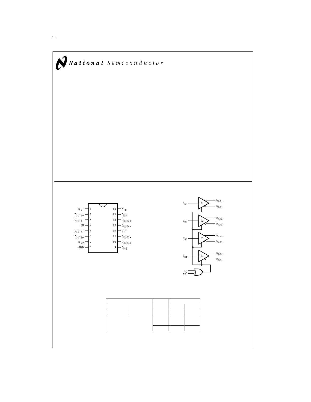
Connection Diagram Functional Diagram
Dual-In-Line
DS100095-1
Order Number DS90LV031ATM
or DS90LV031ATMTC
See NS Package Number M16A or MTC16 or W16A
or DS90LV031AW
DS100095-2
Truth Table
DRIVER
Enables Input Outputs
EN EN
LHXZZ
All other combinations of
ENABLE inputs
TRI-STATE®is a registered trademark of National Semiconductor Corporation.
© 1999 National Semiconductor Corporation DS100095 www.national.com
*
D
D
IN
OUT+DOUT−
LLH
HHL
Absolute Maximum Ratings (Note 1)
If Military/Aerospace specified devices are required,
please contact the National Semiconductor Sales Office/
Distributors for availability and specifications.
Supply Voltage (V
Input Voltage (D
Enable Input Voltage (EN, EN
Output Voltage (D
Short Circuit Duration
(D
OUT+,DOUT−
Maximum Package Power Dissipation
M Package 1088 mW
MTC Package 866 mW
W Package 845 mW
Derate M Package 8.5 mW/˚C above +25˚C
) −0.3V to +4V
CC
) −0.3V to (VCC+ 0.3V)
IN
OUT+,DOUT−
*
) −0.3V to (VCC+ 0.3V)
) −0.3V to +3.9V
) Continuous
@
+25˚C
Storage Temperature Range −65˚C to +150˚C
Lead Temperature Range
Soldering (4 sec.) +260˚C
Maximum Junction Temperature +150˚C
ESD Rating (Note 10)
(HBM, 1.5 kΩ, 100 pF) ≥ 6kV
Recommended Operating
Conditions
Min Typ Max Units
Supply Voltage (V
Operating Free Air
Temperature (T
Industrial −40 +25 +85 ˚C
Military -55 +25 +125 ˚C
) +3.0 +3.3 +3.6 V
CC
)
A
Derate MTC Package 6.9 mW/˚C above +25˚C
Derate W Package 6.8 mW/˚C above +25˚C
Electrical Characteristics
Over supply voltage and operating temperature ranges, unless otherwise specified. (Notes 2, 3, 4)
Symbol Parameter Conditions Pin Min Typ Max Units
V
∆V
V
∆V
V
V
V
V
I
I
V
I
I
I
I
I
I
I
IH
IL
OS
OSD
OFF
OZ
CC
CCL
CCZ
OD1
OS
OH
OL
IH
IL
CL
Differential Output Voltage R
Change in Magnitude of V
OD1
for Complementary Output
OD1
States
Offset Voltage 1.125 1.25 1.375 V
Change in Magnitude of VOSfor
OS
Complementary Output States
Output Voltage High 1.38 1.6 V
Output Voltage Low 0.90 1.03 V
Input Voltage High DIN,
Input Voltage Low GND 0.8 V
Input Current V
Input Current V
Input Clamp Voltage I
Output Short Circuit Current ENABLED, (Note 11)
Differential Output Short Circuit
Current
Power-off Leakage V
Output TRI-STATE Current EN = 0.8V and EN* = 2.0V
No Load Supply Current Drivers
Enabled
Loaded Supply Current Drivers
Enabled
No Load Supply Current Drivers
Disabled
=
Figure 1
L
100Ω (
)D
D
250 350 450 mV
OUT−
OUT+
4 35 |mV|
5 25 |mV|
2.0 V
EN,
D
D
EN*
OUT−
OUT+
±
1 +10 µA
±
1 +10 µA
−6.0 −9.0 mA
−6.0 −9.0 mA
=
or 2.5V −10
V
IN
CC
=
GND or 0.4V −10
IN
=
−18 mA −1.5 −0.8 V
CL
OUT−
=0Vor
=0V
D
IN=VCC,DOUT+
= GND, D
D
IN
ENABLED, VOD=0V
(Note 11)
=
0V or 3.6V,
OUT
=
0V or Open
V
CC
=
0V or V
V
OUT
CC
DIN=VCCor GND V
RL= 100Ω All Channels, DIN=
or GND (all inputs)
V
CC
DIN=VCCor GND,
EN = GND, EN* = V
CC
−20
−10
CC
±
1 +20 µA
±
1 +10 µA
5.0 8.0 mA
23 30 mA
2.6 6.0 mA
CC
V
www.national.com 2
Switching Characteristics - Industrial
=
+3.3V
±
V
CC
Symbol Parameter Conditions Min Typ Max Units
t
PHLD
t
PLHD
t
SKD1
t
SKD2
t
SKD3
t
SKD4
t
TLH
t
THL
t
PHZ
t
PLZ
t
PZH
t
PZL
f
MAX
Differential Propagation Delay High to Low RL= 100Ω,CL=10pF
Differential Propagation Delay Low to High 0.8 1.25 2.0 ns
Differential Pulse Skew |t
(Note 5)
Channel-to-Channel Skew (Note 6) 0 0.1 0.5 ns
Differential Part to Part Skew (Note 7) 0 1.0 ns
Differential Part to Part Skew (Note 8) 0 1.2 ns
Rise Time 0.38 1.5 ns
Fall Time 0.40 1.5 ns
Disable Time High to Z RL= 100Ω,CL=10pF
Disable Time Low to Z 5ns
Enable Time Z to High 7ns
Enable Time Z to Low 7ns
Maximum Operating Frequency (Note 14) 200 250 MHz
10%,T
=
−40˚C to +85˚C (Notes 3, 9, 12)
A
PHLD−tPLHD
Figure 2
and
Figure 3
(
|
)
0 0.07 0.4 ns
5ns
Figure 4
and
Figure 5
0.8 1.18 2.0 ns
(
)
Switching Characteristics - Military
=
+3.3V
±
V
CC
Symbol Parameter Conditions Min Max Units
t
PHLD
t
PLHD
t
SKD1
t
SKD2
t
SKD3
t
SKD4
t
TLH
t
THL
t
PHZ
t
PLZ
t
PZH
t
PZL
f
MAX
Note 1: “Absolute Maximum Ratings” are those values beyond which the safety of the device cannot be guaranteed. They are not meant to imply that the devices
should be operated at these limits. The table of “Electrical Characteristics” specifies conditions of device operation.
Note 2: Current into device pins is defined as positive. Current out of device pins is defined as negative. All voltages are referenced to ground except: V
∆V
OD1
Note 3: All typicals are given for: V
Note 4: The DS90LV031Ais a current mode device and only functions within datasheet specifications when a resistive load is applied to the driver outputs typical
range is (90Ω to 110Ω)
Note 5: t
same channel.
Note 6: t
Note 7: t
fication applies to devices at the same V
Note 8: t
operating temperature and voltage ranges, and across process distribution. t
Note 9: Generator waveform for all tests unless otherwise specified: f=1 MHz, Z
Note 10: ESD Ratings:
Note 11: Output short circuit current (I
Note 12: C
Note 13: All input voltages are for one channel unless otherwise specified. Other inputs are set to GND.
Note 14: f
switching.
Differential Propagation Delay High to Low RL= 100Ω,CL=10pF
Differential Propagation Delay Low to High 0.8 2.0 ns
Differential Pulse Skew |t
(Note 5)
Channel-to-Channel Skew (Note 6) 0 0.5 ns
Differential Part to Part Skew (Note 7) 0 1.0 ns
Differential Part to Part Skew (Note 8) 0 1.2 ns
Rise Time 1.5 ns
Fall Time 1.5 ns
Disable Time High to Z RL= 100Ω,CL=10pF
Disable Time Low to Z 5ns
Enable Time Z to High 7ns
Enable Time Z to Low 7ns
Maximum Operating Frequency (Note 14) 200 MHz
.
,|t
SKD1
PHLD−tPLHD
is the Differential Channel-to-Channel Skew of any event on the same device.
SKD2
, Differential Part to Part Skew, is defined as the difference between the minimum and maximum specified differential propagation delays. This speci-
SKD3
, part to part skew, is the differential channel-to-channel skew of any event between devices. This specification applies to devices over recommended
SKD4
HBM (1.5 kΩ, 100 pF) ≥ 6kV
includes probe and jig capacitance.
L
generator input conditions: t
MAX
=
10%,T
−55˚C to +125˚C (Notes 9, 12)
A
0.8 2.0 ns
Figure 2
and
Figure 3
Figure 5
)
0 0.4 ns
)
(
+25˚C.
|
Figure 4
=
50Ω,t
O
and
≤1 ns, and tf≤ 1 ns.
r
(
is defined as |Max − Min| differential propagation delay.
SKD4
PHLD−tPLHD
=
CC
| is the magnitude difference in differential propagation delay time between the positive going edge and the negative going edge of the
OS
=
+3.3V, T
A
and within 5˚C of each other within the operating temperature range.
CC
) is specified as magnitude only, minus sign indicates direction only.
=
<
1ns, (0%to 100%), 50%duty cycle, 0V to 3V.Output Criteria: duty cycle=45%/55%, VOD>250mV,all channels
t
r
f
5ns
and
OD1
www.national.com3
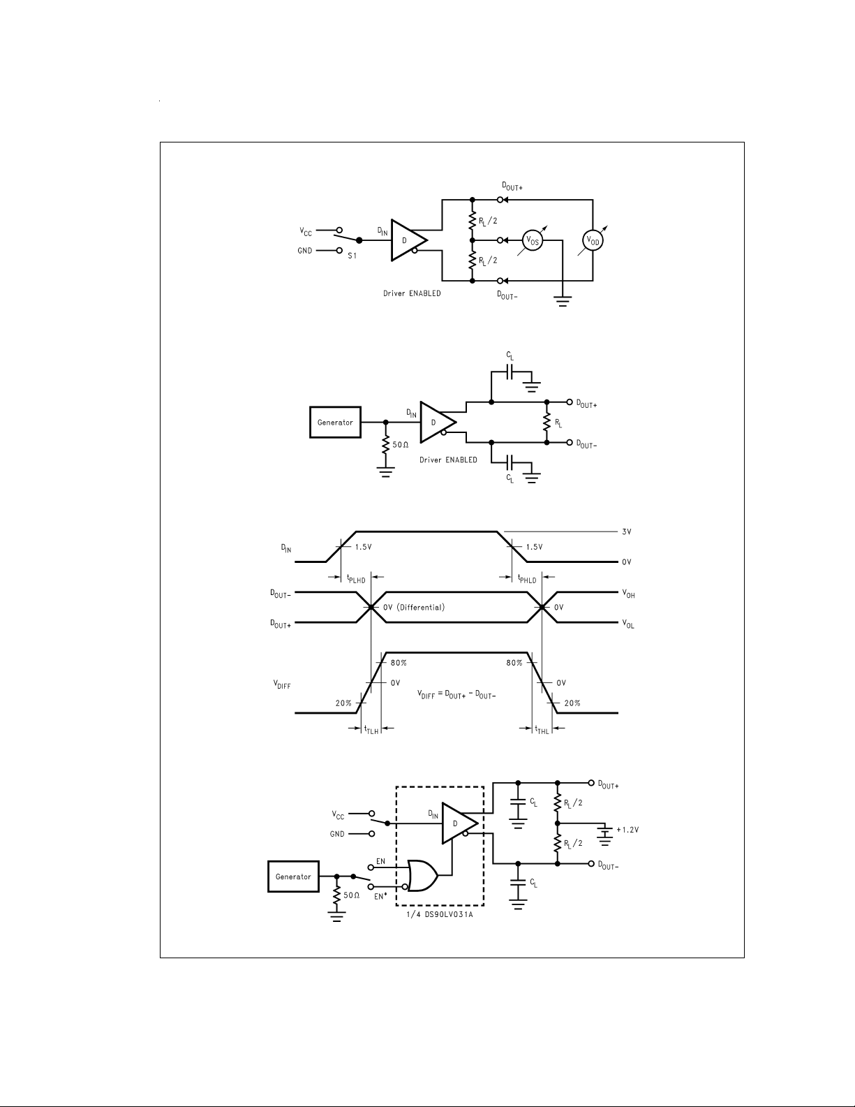
Parameter Measurement Information
FIGURE 1. Driver VODand VOSTest Circuit
FIGURE 2. Driver Propagation Delay and Transition Time Test Circuit
DS100095-3
DS100095-4
FIGURE 3. Driver Propagation Delay and Transition Time Waveforms
FIGURE 4. Driver TRI-STATE Delay Test Circuit
www.national.com 4
DS100095-5
DS100095-6

Parameter Measurement Information (Continued)
FIGURE 5. Driver TRI-STATE Delay Waveform
Typical Application
DS100095-7
FIGURE 6. Point-to-Point Application
Applications Information
General application guidelines and hints for LVDS drivers
and receivers may be found in the following application
notes: LVDS Owner’s Manual (lit #550062-001), AN808,
AN1035, AN977, AN971, AN916, AN805, AN903.
LVDSdrivers and receivers are intended to be primarily used
in an uncomplicated point-to-point configuration as is shown
in
Figure 6
vironment for the quick edge rates of the drivers. The receiver is connected to the driver through a balanced media
which may be a standard twisted pair cable, a parallel pair
cable, or simply PCB traces. Typically, the characteristic differential impedance of the media is in the range of 100Ω.A
termination resistor of 100Ω should be selected to match the
media, and is located as close to the receiver input pins as
possible. The termination resistor converts the current
sourced bythe driver into a voltagethat is detected by thereceiver. Other configurations are possible such as a
multi-receiver configuration, but the effects of a mid-stream
connector(s), cable stub(s), and other impedance discontinuities as well as ground shifting, noise margin limits, and total termination loading must be taken into account.
The DS90LV031A differential line driver is a balanced current source design. A current mode driver, generally speaking has a high output impedance and supplies a constant
current for a range of loads (a voltage mode driver on the
other hand supplies a constant voltage for a range ofloads).
Current is switched through the load in one direction to pro-
. This configuration provides a clean signaling en-
DS100095-8
duce a logic state and in the other direction to produce the
other logic state. The output current is typically 3.5 mA, a
minimum of 2.5 mA, and a maximum of 4.5 mA. The current
mode requires (as discussed above) that a resistive termination be employed to terminate the signal and to complete
the loop as shown in
Figure 6
. AC or unterminated configurations are not allowed. The 3.5 mA loop current will develop
a differential voltage of 350 mV across the 100Ω termination
resistor which the receiver detects with a 250 mV minimum
differential noise margin neglecting resistive line losses
(driven signal minus receiver threshold (350 mV – 100 mV
250 mV)). The signal is centered around +1.2V (Driver Offset, V
) with respect to ground as shown in
OS
that the steady-state voltage (V
twice the differential voltage (V
) peak-to-peak swing is
SS
) and is typically 700 mV.
OD
Figure 7
. Note
The current mode driver provides substantial benefits over
voltage mode drivers, such as an RS-422 driver. Its quiescent current remains relatively flat versus switching frequency.Whereas the RS-422 voltage mode driverincreases
exponentially in most case between 20 MHz–50 MHz. This
is due to the overlap current that flows between the rails of
the device when the internal gates switch. Whereas the current mode driver switches a fixed current between its output
without any substantial overlap current. This is similar to
some ECL and PECL devices, but without the heavy static
I
requirements of the ECL/PECL designs. LVDS requires
CC
>
80%less current than similar PECLdevices. AC specifications for the driver are a tenfold improvement over other existing RS-422 drivers.
www.national.com5
=

Applications Information (Continued)
The TRI-STATE function allows the driver outputs to be disabled, thus obtaining an even lower power state when the
transmission of data is not required.
The footprint of the DS90LV031Ais the same as the industry
standard 26LS31 Quad Differential (RS-422) Driver and is a
step down replacement for the 5V DS90C031 Quad Driver.
Power Decoupling Recommendations:
Bypass capacitors must be used on power pins. High frequency ceramic (surface mount is recommended) 0.1µF in
parallel with 0.01µF, in parallel with 0.001µF at the power
supply pin as well as scattered capacitors over the printed
circuit board. Multiple vias should be used to connect the decoupling capacitors to the power planes. A 10µF (35V) or
greater solid tantalum capacitor should be connected at the
power entry point on the printed circuit board.
PC Board considerations:
Use at least 4 PCB layers (top to bottom); LVDS signals,
ground, power, TTL signals.
Isolate TTL signals from LVDS signals, otherwise the TTL
may couple onto the LVDS lines. It is best to put TTL and
LVDS signals on different layers which are isolated by a
power/ground plane(s).
Keep drivers and receivers as close to the (LVDS port side)
connectors as possible.
Differential Traces:
Use controlled impedance traces which match the differential impedance of your transmission medium (ie. cable) and
termination resistor. Run the differential pair trace lines as
close together as possible as soon as they leave the IC
(stubs should be
flections and ensure noise is coupled as common-mode. In
fact, we have seen that differential signals which are 1mm
apart radiate far less noise than traces 3mm apart since
magnetic field cancellation is much better with the closer
traces. Plus, noise induced on the differential lines is much
more likely to appear as common-mode which is rejected by
the receiver.
Match electrical lengths between traces to reduce skew.
Skew between the signals of a pair means a phase difference between signals which destroys the magnetic field cancellation benefits of differential signals and EMI will result.
(Note the velocity of propagation, v = c/Er where c (the
speed of light) = 0.2997mm/ps or 0.0118 in/ps). Do not rely
solely on the autoroute function for differential traces. Carefully review dimensions to match differential impedance and
provide isolation for the differential lines. Minimize the number or vias and other discontinuities on the line.
Avoid 90˚ turns (these cause impedance discontinuities).
Use arcs or 45˚ bevels.
Within a pair of traces, the distance between the two traces
should be minimized to maintain common-mode rejection of
the receivers. On the printed circuit board, this distance
should remain constant to avoid discontinuities indifferential
impedance. Minor violations at connection points are allowable.
<
10mm long). This will help eliminate re-
Termination:
Use aresistor which best matches the differential impedance
or your transmission line. The resistor should be between
90Ω and 130Ω. Remember that the current mode outputs
need the termination resistor to generate the differential voltage. LVDS will not work without resistor termination. Typically,connect a single resistor across the pairat the receiver
end.
Surface mount 1%to 2%resistors are best. PCB stubs,
component lead, and the distance from the termination to the
receiver inputs should be minimized. The distance between
the termination resistor and the receiver should be
(12mm MAX).
Probing LVDS Transmission Lines:
Always use high impedance (
<
(
2pF) scope probes with a wide bandwidth (1GHz) scope.
Improper probing will give deceiving results.
Cables and Connectors, General Comments:
When choosing cable and connectors for LVDS it is important to remember:
Use controlled impedance media. The cables and connectors you use should have a matched differential impedance
of about 100Ω. They should not introduce major impedance
discontinuities.
Balanced cables (e.g. twisted pair) are usually better than
unbalanced cables (ribbon cable, simple coax.) for noise reduction and signal quality. Balanced cables tend to generate
less EMI due to field canceling effects and also tend to pick
up electromagnetic radiation a common-mode (not differential mode) noise which is rejected by the receiver. For cable
distances
tively. For distances 0.5M ≤ d ≤ 10M, CAT 3 (category 3)
twisted pair cable works well, is readily available and relatively inexpensive.
Fail-safe Feature:
The LVDS receiver is a high gain, high speed device that
amplifies a small differential signal (20mV) to CMOS logic
levels. Due to the high gain and tight threshold of the receiver,care should be taken to prevent noise from appearing
as a valid signal.
The receiver’s internal fail-safe circuitry is designed to
source/sink a small amount of current, providing fail-safe
protection (a stable known state of HIGH output voltage) for
floating, terminated or shorted receiver inputs.
1. Open Input Pins. The DS90LV032A is a quad receiver
2. Terminated Input. If the driver is disconnected (cable
<
0.5M, most cables can be made to work effec-
device, and if an application requires only 1, 2 or 3 receivers, the unused channel(s) inputs should be left
OPEN. Do not tie unused receiver inputs to ground or
any other voltages. The input is biased by internal high
value pull up and pull down resistors to set the output to
a HIGH state. This internal circuitry will guarantee a
HIGH, stable output state for open inputs.
unplugged), or if the driver is in a TRI-STATE or poweroff condition, the receiver output will again be in a HIGH
state, even with the end of cable 100Ω termination resistor across the input pins. The unplugged cable can become a floating antenna which can pick up noise. If the
cable picks up more than 10mV of differential noise, the
receiver may see the noise as a valid signal and switch.
To insure that any noise is seen as common-mode and
not differential, a balanced interconnect should be used.
Twisted pair cable will offer better balance than flat ribbon cable.
>
100kΩ), low capacitance
<
10mm

Applications Information (Continued)
3. Shorted Inputs. If a fault condition occurs that shorts
the receiver inputs together, thus resulting in a 0V differential input voltage, the receiver output will remain in a
HIGH state. Shorted input fail-safe is not supported
across the common-mode range of the device (GND to
2.4V). It is only supported with inputs shorted and no external common-mode voltage applied.
FIGURE 7. Driver Output Levels
External lower value pull up and pull down resistors (for a
stronger bias) may be used to boost fail-safe in the presence
of higher noise levels. The pull up and pull down resistors
should be in the 5kΩ to 15kΩ range to minimize loading and
waveform distortion to the driver. The common-mode bias
point should be set to approximately 1.2V (less than 1.75V)
to be compatible with the internal circuitry.
DS100095-9
Pin Descriptions
Pin No. Name Description
1, 7, 9, 15 D
2, 6, 10,14D
3, 5, 11,13D
Driver input pin, TTL/CMOS
IN
compatible
Non-inverting driver output pin,
OUT+
LVDS levels
Inverting driver output pin, LVDS
OUT−
levels
4 EN Active high enable pin, OR-ed
*
with EN
12 EN*Active low enable pin, OR-ed
with EN
16 V
Power supply pin, +3.3V±0.3V
CC
8 GND Ground pin
Ordering Information
Operating Package Type/ Order Number
Temperature Number
−40˚C to +85˚C SOP/M16A DS90LV031ATM
−40˚C to +85˚C TSSOP/MTC16 DS90LV031ATMTC
Operating Package Type/ Order Number
Temperature Number
-55˚C to +125˚C Cerpack/W16A DS90LV031AW-QML
DS100095-10
FIGURE 8. Typical DS90LV031A, D
vs R
L,TA
= 25˚C
(single ended)
OUT
www.national.com7

Applications Information (Continued)
FIGURE 9. Typical DS90LV031A, D
V
= 3.3V, TA= 25˚C
CC
DS100095-11
vs RL,
OUT
www.national.com 8

Physical Dimensions inches (millimeters) unless otherwise noted
16-Lead (0.150" Wide) Molded Small Outline Package, JEDEC
Order Number DS90LV031ATM
NS Package Number M16A
www.national.com9

Physical Dimensions inches (millimeters) unless otherwise noted (Continued)
16-Lead (0.100" Wide) Molded Thin Shrink Small Outline Package, JEDEC
www.national.com 10
Order Number DS90LV031ATMTC
NS Package Number MTC16

Physical Dimensions inches (millimeters) unless otherwise noted (Continued)
DS90LV031A 3V LVDS Quad CMOS Differential Line Driver
Order Number DS90LV031AW-QML
16-Lead Cerpack
NS Package Number W16A
LIFE SUPPORT POLICY
NATIONAL’S PRODUCTS ARE NOT AUTHORIZED FOR USE AS CRITICAL COMPONENTS IN LIFE SUPPORT
DEVICES OR SYSTEMS WITHOUT THE EXPRESS WRITTEN APPROVAL OF THE PRESIDENT AND GENERAL
COUNSEL OF NATIONAL SEMICONDUCTOR CORPORATION. As used herein:
1. Life support devices or systems are devices or
systems which, (a) are intended for surgical implant
into the body, or (b) support or sustain life, and
whose failure to perform when properly used in
accordance with instructions for use provided in the
2. A critical component is any component of a life
support device or system whose failure to perform
can be reasonably expected to cause the failure of
the life support device or system, or to affect its
safety or effectiveness.
labeling, can be reasonably expected to result in a
significant injury to the user.
National Semiconductor
Corporation
Americas
Tel: 1-800-272-9959
Fax: 1-800-737-7018
Email: support@nsc.com
www.national.com
National Semiconductor
Europe
Fax: +49 (0) 1 80-530 85 86
Email: europe.support@nsc.com
Deutsch Tel: +49 (0) 1 80-530 85 85
English Tel: +49 (0) 1 80-532 78 32
Français Tel: +49 (0) 1 80-532 93 58
Italiano Tel: +49 (0) 1 80-534 16 80
National Semiconductor
Asia Pacific Customer
Response Group
Tel: 65-2544466
Fax: 65-2504466
Email: sea.support@nsc.com
National Semiconductor
Japan Ltd.
Tel: 81-3-5639-7560
Fax: 81-3-5639-7507
National does not assume any responsibility for use of any circuitry described, no circuit patent licenses are implied and National reserves the right at any time without notice to change said circuitry and specifications.
 Loading...