

DS90CR483A / DS90CR484A
48-Bit LVDS Channel Link SER/DES – 33 - 112 MHz
General Description
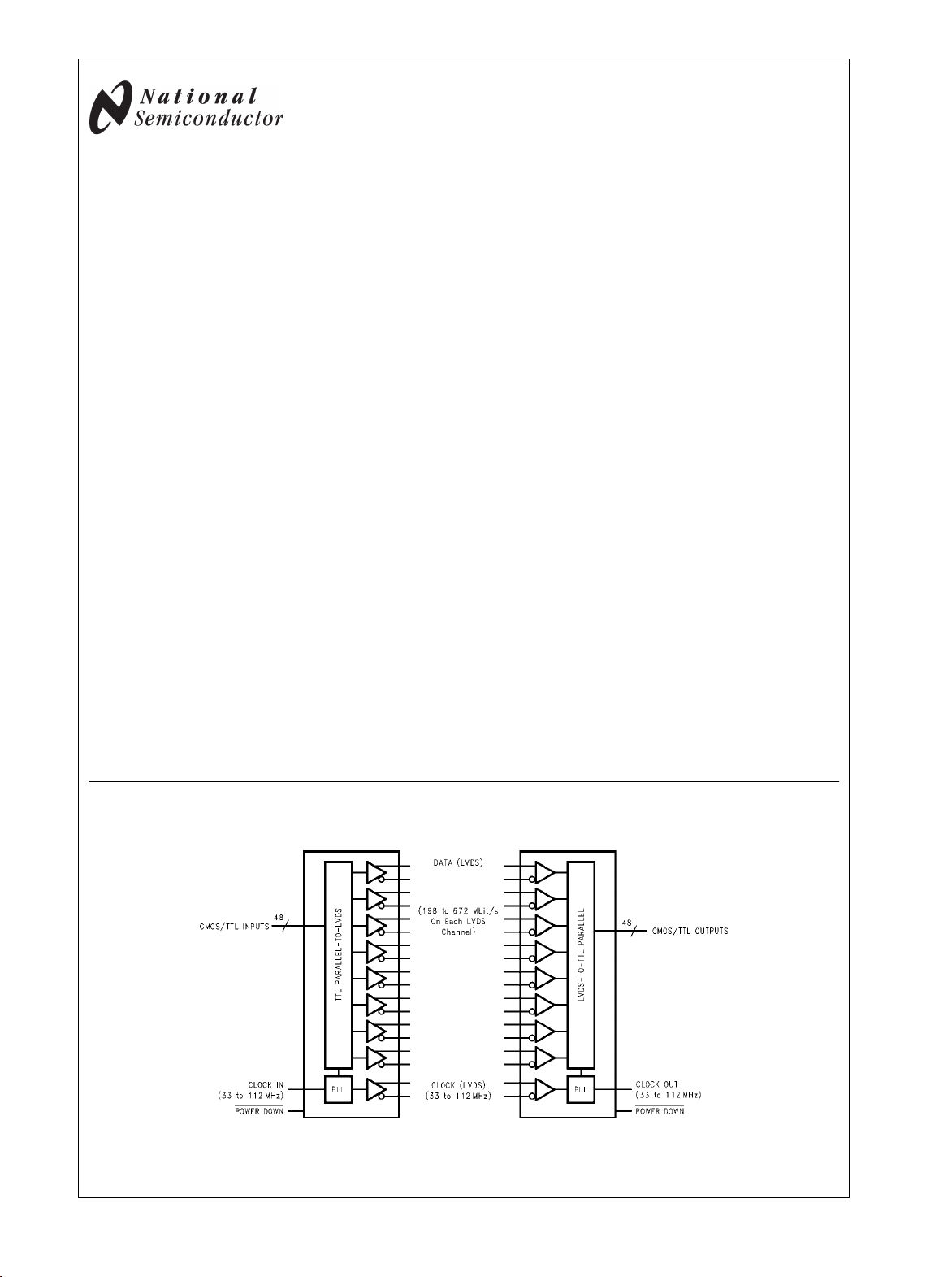
The DS90CR483A transmitter converts 48 bits of CMOS/TTL
data into eight LVDS (Low Voltage Differential Signaling) data
streams. A phase-locked transmit clock is transmitted in parallel with the data streams over a ninth LVDS link. Every cycle
of the transmit clock 48 bits of input data are sampled and
transmitted. The DS90CR484A receiver converts the LVDS
data streams back into 48 bits of CMOS/TTL data. At a transmit clock frequency of 112MHz, 48 bits of TTL data are
transmitted at a rate of 672Mbps per LVDS data channel. Using a 112MHz clock, the data throughput is 5.38Gbit/s (672Mbytes/s).
The multiplexing of data lines provides a substantial cable reduction. Long distance parallel single-ended buses typically
require a ground wire per active signal (and have very limited
noise rejection capability). Thus, for a 48-bit wide data and
one clock, up to 98 conductors are required. With this Channel
Link chipset as few as 19 conductors (8 data pairs, 1 clock
pair and a minimum of one ground) are needed. This provides
an 80% reduction in cable width, which provides a system
cost savings, reduces connector physical size and cost, and
reduces shielding requirements due to the cables' smaller
form factor.
The 48 CMOS/TTL inputs can support a variety of signal
combinations. For example, 6 8-bit words or 5 9-bit (byte +
parity) and 3 controls.
The DS90CR483A/DS90CR484A chipset is improved over
prior generations of Channel Link devices and offers higher
bandwidth support and longer cable drive with three areas of
enhancement. To increase bandwidth, the maximum clock
rate is increased to 112 MHz and 8 serialized LVDS outputs
are provided. Cable drive is enhanced with a user selectable
pre-emphasis feature that provides additional output current
during transitions to counteract cable loading effects. Optional DC balancing on a cycle-to-cycle basis, is also provided to
reduce ISI (Inter-Symbol Interference). With pre-emphasis
and DC balancing, a low distortion eye-pattern is provided at
the receiver end of the cable. A cable deskew capability has
been added to deskew long cables of pair-to-pair skew of up
to +/−1 LVDS data bit time (up to 80 MHz Clock Rate). These
three enhancements allow cables 5+ meters in length to be
driven.
The chipset is an ideal means to solve EMI and cable size
problems associated with wide, high speed TTL interfaces.
For more details, please refer to the “Applications Information” section of this datasheet.
Features
Up to 5.38 Gbits/sec bandwidth
■
33 MHz to 112 MHz input clock support
■
LVDS SER/DES reduces cable and connector size
■
Pre-emphasis reduces cable loading effects
■
DC balance data transmission provided by transmitter
■
reduces ISI distortion
Cable Deskew of +/−1 LVDS data bit time (up to 80 MHz
■
Clock Rate)
5V Tolerant TxIN and control input pins
■
Flow through pinout for easy PCB design
■
+3.3V supply voltage
■
Transmitter rejects cycle-to-cycle jitter
■
Conforms to ANSI/TIA/EIA-644-1995 LVDS Standard
■
Both devices are available in 100 lead TQFP package
■
DS90CR483A/DS90CR484A 48-Bit LVDS Channel Link SER/DES — 33 - 112 MHz
April 4, 2008
Generalized Block Diagrams
30059201
© 2008 National Semiconductor Corporation 300592 www.national.com

Generalized Transmitter Block Diagram
DS90CR483A/DS90CR484A
Generalized Receiver Block Diagram
30059202
Ordering Information
Order Number Function Package
DS90CR483AVJD Transmitter (Serializer) VJD100A
DS90CR484AVJD Receiver (Deserializer) VJD100A
www.national.com 2
30059203

DS90CR483A/DS90CR484A
Absolute Maximum Ratings (Note 1)
If Military/Aerospace specified devices are required,
please contact the National Semiconductor Sales Office/
Distributors for availability and specifications.
Supply Voltage (VCC)
CMOS/TTL Input Voltage −0.3V to +5.5V
LVCMOS/TTL Output
Voltage
−0.3V to (VCC + 0.3V)
LVDS Receiver Input
Voltage −0.3V to +3.6V
LVDS Driver Output
Voltage −0.3V to +3.6V
LVDS Output Short
Circuit Duration Continuous
Junction Temperature +150°C
Storage Temperature −65°C to +150°C
Lead Temperature
(Soldering, 4 sec.)
100L TQFP +260°C
Maximum Package Power Dissipation Capacity @ 25°
C
100 TQFP Package:
DS90CR483AVJD 2.3W
−0.3V to +4V
DS90CR484AVJD 2.3W
Package Derating:
DS90CR483AVJD 18.1mW/°C above +25°C
DS90CR484AVJD 18.1mW/°C above +25°C
ESD Rating:
DS90CR483A
(HBM, 1.5kΩ, 100pF) > 6 kV
(EIAJ, 0Ω, 200pF) > 300 V
DS90CR484A
(HBM, 1.5kΩ, 100pF) > 2 kV
(EIAJ, 0Ω, 200pF) > 200 V
Recommended Operating Conditions
Min Nom Max Units
Supply Voltage (VCC) 3.0 3.3 3.6 V
Operating Free Air
Temperature (T
A)
Receiver Input Range 0 2.4 V
Supply Noise Voltage 100 mV
Input Clock (TX) 33 112 MHz
−10 +25 +70 °C
Electrical Characteristics
Over recommended operating supply and temperature ranges unless otherwise specified.
Symbol Parameter Conditions Min Typ Max Units
CMOS/TTL DC SPECIFICATIONS
V
IH
V
IL
V
OH
V
OL
V
CL
I
IN
I
OS
High Level Input Voltage 2.0 V
Low Level Input Voltage GND 0.8 V
High Level Output
Voltage
IOH = −0.4 mA 2.7 3.3 V
IOH = −2mA 2.7 2.85 V
Low Level Output Voltage IOL = 2 mA 0.1 0.3 V
Input Clamp Voltage ICL = −18 mA −0.79 −1.5 V
Input Current VIN = 0.4V, 2.5V or V
CC
+1.8 +15 µA
VIN = GND −15 0 µA
Output Short Circuit
V
= 0V −120 mA
OUT
Current
p-p
3 www.national.com

Symbol Parameter Conditions Min Typ Max Units
LVDS DRIVER DC SPECIFICATIONS
|VOD| Differential Output
RL = 100Ω
250 345 450 mV
Voltage
ΔV
OD
Change in VOD between
35 mV
Complimentary Output
States
V
OS
ΔV
OS
DS90CR483A/DS90CR484A
I
OS
Offset Voltage 1.125 1.25 1.375 V
Change in VOS between
35 mV
Complimentary Output
States
Output Short Circuit
V
= 0V, RL = 100Ω
OUT
−3.5 −5 mA
Current
I
OZ
Output TRI-STATE
PD = 0V, V
= 0V or V
OUT
CC
±1 ±10 µA
Current
LVDS RECEIVER DC SPECIFICATIONS
V
TH
Differential Input High
VCM = +1.2V +100 mV
Threshold
V
TL
Differential Input Low
−100 mV
Threshold
I
IN
Input Current VIN = +2.4V, VCC = 3.6V ±10 µA
VIN = 0V, VCC = 3.6V ±10 µA
TRANSMITTER SUPPLY CURRENT
ICCTW Transmitter Supply
Current
Worst Case
RL = 100Ω, CL = 5 pF,
BAL = High,
Worst Case Pattern
f = 33 MHz 91.4 140 mA
f = 66 MHz 106 160 mA
f = 112 MHz 155 210 mA
(Figures 1, 2)
ICCTZ Transmitter Supply
Current
Power Down
PD = Low 5 50 µA
Driver Outputs in TRI-STATE during power down
Mode
RECEIVER SUPPLY CURRENT
ICCRW Receiver Supply Current
Worst Case
ICCRZ Receiver Supply Current
Power Down
CL = 8 pF, BAL = High,
Worst Case Pattern
(Figures 1, 3)
f = 33 MHz 125 150 mA
f = 66 MHz 200 210 mA
f = 112 MHz 250 280 mA
PD = Low
Receiver Outputs stay low during power down mode.
20 100 µA
Recommended Transmitter Input Characteristics
Over recommended operating supply and temperature ranges unless otherwise specified.
Symbol Parameter Min Typ Max Units
TCIT TxCLK In Transition Time (Figure 4) 1.0 2.0 3.0 ns
TCIP High TxCLK In Period, PLLSEL = High Gear (Figure 5) 8.928 T 26.3 ns
TCIP Low TxCLK In Period, PLLSEL = Low Gear (Figure 5) 25 T 30.3 ns
TCIH TxCLK In High Time (Figure 5) 0.35T 0.5T 0.65T ns
TCIL TxCLK In Low Time (Figure 5) 0.35T 0.5T 0.65T ns
TXIT TxIN Transition Time 1.5 6.0 ns
www.national.com 4

Transmitter Switching Characteristics
Over recommended operating supply and temperature ranges unless otherwise specified.
Symbol Parameter Min Typ Max Units
LLHT LVDS Low-to-High Transition Time, (Figure 2),
PRE = 0.75V (disabled)
LVDS Low-to-High Transition Time, (Figure 2),
PRE = Vcc (max)
LHLT LVDS High-to-Low Transition Time, (Figure 2),
PRE = 0.75V (disabled)
LVDS High-to-Low Transition Time, (Figure 2),
PRE = Vcc (max)
TBIT Transmitter Bit Width 1/7 TCIP ns
TPPOS Transmitter Pulse Positions - Normalized f = 33 to 70
MHz
f = 70 to 112
MHz
TJCC Transmitter Jitter - Cycle-to-Cycle ((Note 8) 50 100 ps
TCCS TxOUT Channel to Channel Skew 40 ps
TSTC TxIN Setup to TxCLK IN, (Figure 5) 2.5 ns
THTC TxIN Hold to TxCLK IN, (Figure 5) 0 ns
TPDL Transmitter Propagation Delay - Latency, (Figure 7) 1.5(TCIP)+3.72 1.5(TCIP)+4.4 1.5(TCIP)+6.24 ns
TPLLS Transmitter Phase Lock Loop Set, (Figure 9) 10 ms
TPDD Transmitter Powerdown Delay, (Figure 11) 100 ns
0.14 0.7 ns
0.11 0.6 ns
0.16 0.8 ns
0.11 0.7 ns
−250 0 +250 ps
−200 0 +200 ps
DS90CR483A/DS90CR484A
Receiver Switching Characteristics
Over recommended operating supply and temperature ranges unless otherwise specified.
Symbol Parameter Min Typ Max Units
CLHT CMOS/TTL Low-to-High Transition Time, (Figure 3), Rx
data out
CMOS/TTL Low-to-High Transition Time, (Figure 3), Rx
clock out
CHLT CMOS/TTL High-to-Low Transition Time, (Figure 3), Rx
data out
CMOS/TTL High-to-Low Transition Time, (Figure 3), Rx
clock out
RCOP RxCLK OUT Period, (Figure 6) 8.928 T 30.3 ns
RCOH RxCLK OUT High Time, (Figure 6),
(Note 4)
RCOL RxCLK OUT Low Time, (Figure 6),
(Note 4)
RSRC RxOUT Setup to RxCLK OUT, (Figure
6), (Note 4)
RHRC RxOUT Hold to RxCLK OUT, (Figure
6), (Note 4)
RPDL Receiver Propagation Delay - Latency, (Figure 8) 3(TCIP)+4.0 3(TCIP)+4.8 3(TCIP)+6.5 ns
RPLLS Receiver Phase Lock Loop Set, (Figure 10) 10 ms
RPDD Receiver Powerdown Delay, (Figure 12) 1 µs
f = 112 MHz 3.5 ns
f = 66 MHz 6.0 ns
f = 112 MHz 3.5 ns
f = 66 MHz 6.0 ns
f = 112 MHz 2.4 ns
f = 66 MHz 3.6 ns
f = 112 MHz 3.4 ns
f = 66 MHz 7.0 ns
2.0 ns
1.0 ns
2.0 ns
1.0 ns
5 www.national.com

Chipset RSKM Characteristics
Over recommended operating supply and temperature ranges unless otherwise specified.(Notes 4, 7). See Applications Information section for more details on this parameter and how to apply it.
Symbol Parameter Min Typ Max Units
RSKM Receiver Skew Margin without Deskew
in non-DC Balance Mode, (Figure 13),
(Note 5)
RSKM Receiver Skew Margin without Deskew
DS90CR483A/DS90CR484A
in DC Balance Mode, (Figure 13),
(Note 5)
RSKMD Receiver Skew Margin with Deskew in
DC Balance, (Figure 14),
(Note 6)
RDR Receiver Deskew Range f = 80 MHz ±1 TBIT
RDSS Receiver Deskew Step Size f = 80 MHz 0.3TBIT ns
Note 1: “Absolute Maximum Ratings” are those values beyond which the safety of the device cannot be guaranteed. They are not meant to imply that the device
should be operated at these limits. The tables of “Electrical Characteristics” specify conditions for device operation.
Note 2: Typical values are given for VCC = 3.3V and T A = +25°C.
Note 3: Current into device pins is defined as positive. Current out of device pins is defined as negative. Voltages are referenced to ground unless otherwise
specified (except VTH, VTL, VOD and ΔVOD).
Note 4: The Minimum and Maximum Limits are based on statistical analysis of the device performance over voltage and temperature ranges. This parameter is
functionally tested on Automatic Test Equipment (ATE). ATE is limited to 85MHz. A sample of characterization parts have been bench tested to verify functional
performance.
Note 5: Receiver Skew Margin (RSKM) is defined as the valid data sampling region at the receiver inputs. This margin takes into account transmitter output pulse
positions (min and max) and the receiver input setup and hold time (internal data sampling window - RSPOS). This margin allows for LVDS interconnect skew,
inter-symbol interference (both dependent on type/length of cable) and clock jitter.
RSKM ≥ cable skew (type, length) + source clock jitter (cycle to cycle, TJCC) + ISI (if any). See Applications Information section for more details.
Note 6: Receiver Skew Margin with Deskew (RSKMD) is defined as the valid data sampling region at the receiver inputs. The DESKEW function will constrain
the receiver’s sampling strobes to the middle half of the LVDS bit and removes (adjusts for) fixed interconnect skew. This margin (RSKMD) allows for inter-symbol
interference (dependent on type/length of cable), Transmitter Pulse Position (TPPOS) variance, and LVDS clock jitter (TJCC).
RSKMD ≥ ISI + TPPOS(variance) + source clock jitter (cycle to cycle). See Applications Information section for more details.
Note 7: Typical values for RSKM and RSKMD are applicable for fixed VCC and T A for the Transmitter and Receiver (both are assumed to be at the same V
and T A points).
Note 8: TJCC is a function of input clock quality and also PLLVCC noise. At 112MHz operation, with a +/−300ps input impulse at a 2us rate, TJCC has been
measured to be in the 70-80ps range (<100ps). With a nominal input clock quality (no input impulse jitter, jitter < 500kHz), TJCC is typically 50ps or less. For
RSKM/RSKMD calculations 100ps is typically used as the TJCC budget. See Clock Jitter discussion in the Applications Information section of this datasheet for
further information.
f = 112 MHz 170 ps
f = 100 MHz 170 240 ps
f = 85MHz 300 350 ps
f = 66MHz 300 350 ps
f = 112 MHz 170 ps
f = 100 MHz 170 200 ps
f = 85 MHz 250 300 ps
f = 66 MHz 250 300 ps
f = 50MHz 300 350 ps
f = 33 to 80 MHz 0.25TBIT ps
CC
www.national.com 6

AC Timing Diagrams
FIGURE 1. “Worst Case” Test Pattern
Note 9: The worst case test pattern produces a maximum toggling of digital circuits, LVDS I/O and CMOS/TTL I/O.
DS90CR483A/DS90CR484A
30059210
30059212
FIGURE 2. DS90CR483A (Transmitter) LVDS Output Load and Transition Times
FIGURE 3. DS90CR484A (Receiver) CMOS/TTL Output Load and Transition Times
30059214
FIGURE 4. DS90CR483A (Transmitter) Input Clock Transition Time
30059213
7 www.national.com

DS90CR483A/DS90CR484A
FIGURE 5. DS90CR483A (Transmitter) Setup/Hold and High/Low Times
FIGURE 6. DS90CR484A (Receiver) Setup/Hold and High/Low Times
30059215
30059216
FIGURE 7. DS90CR483A (Transmitter) Propagation Delay - Latency
www.national.com 8
30059227

30059228
FIGURE 8. DS90CR484A (Receiver) Propagation Delay - Latency
DS90CR483A/DS90CR484A
FIGURE 9. DS90CR483A (Transmitter) Phase Lock Loop Set Time
30059219
30059220
FIGURE 10. DS90CR484A (Receiver) Phase Lock Loop Set Time
9 www.national.com

DS90CR483A/DS90CR484A
30059221
FIGURE 11. DS90CR483A (Transmitter) Power Down Delay
30059222
FIGURE 12. DS90CR484A (Receiver) Power Down Delay
www.national.com 10

DS90CR483A/DS90CR484A
C — Setup and Hold Time (Internal data sampling window) defined by Rspos (receiver input strobe position) min and max
TPPOS — Transmitter output pulse position (min and max)
RSKM ≥ Cable Skew (type, length) + LVDS Source Clock Jitter (cycle to cycle) + ISI (Inter-symbol interference)
■ Cable Skew — typically 10 ps to 40 ps per foot, media dependent
■ TJCC — Cycle-to-cycle LVDS Output jitter (TJCC) is less than 100 ps (worse case estimate).
■ ISI is dependent on interconnect length; may be zero
■ See Applications Informations section for more details.
FIGURE 13. Receiver Skew Margin (RSKM) without DESKEW
C — Setup and Hold Time (Internal data sampling window) defined by Rspos (receiver input strobe position) min and max
RSKMD ≥ TPPOSvariance (d) + TJCC (output jitter)(f) + ISI (m)
■ d = Tppos — Transmitter output pulse position (min and max)
■ f = TJCC — Cycle-to-cycle LVDS Output jitter (TJCC) is less than 100 ps (worse case estimate).
■ m = extra margin - assigned to ISI in long cable applications
See Applications Informations section for more details.
30059225
30059229
FIGURE 14. Receiver Skew Margin (RSKMD)with DESKEW
11 www.national.com

LVDS Interface
DS90CR483A/DS90CR484A
Optional features supported: Pre-emphasis, and Deskew
FIGURE 15. 48 Parallel TTL Data Bits Mapped to LVDS Outputs with DC Balance Enabled
30059204
www.national.com 12

DS90CR483A/DS90CR484A
Optional feature supported: Pre-emphasis
FIGURE 16. 48 Parallel TTL Data Bits Mapped to LVDS Outputs with DC Balance Disabled
30059205
13 www.national.com

Applications Information
The DS90CR483A and DS90CR484A are upgrades to the
DS90CR483 and DS90CR484. The DS90CR483A/
DS90CR484A no longer have a PLL auto gear option selectable via the PLLSEL pin. The PLLSEL pin now allows for
the PLL low gear only or high gear only to be selected. The
DS90CR483A/DS90CR484A are fully compatible with older
generation Channel Link devices. It should be noted that
whenever devices with the auto gear feature are used, an
unintentional gear shift caused by fluctuations in VCC may
cause bit errors. By removing the auto gear feature in the
DS90CR483A/DS90CR484A, the potential for any gear shift
DS90CR483A/DS90CR484A
related bit errors has been eliminated.
The DS90CR483A/DS90CR484A chipset is improved over
prior generations of Channel Link devices and offers higher
bandwidth support and longer cable drive with three areas of
enhancement. To increase bandwidth, the maximum clock
rate is increased to 112 MHz and 8 serialized LVDS outputs
are provided. Cable drive is enhanced with a user selectable
pre-emphasis feature that provides additional output current
during transitions to counteract cable loading effects. This requires the use of one pull up resistor to Vcc; please refer to
to set the level needed. Optional DC balancing on a cycle-tocycle basis, is also provided to reduce ISI (Inter-Symbol Interference). With pre-emphasis and DC balancing, a low
distortion eye-pattern is provided at the receiver end of the
cable. A cable deskew capability has been added to deskew
TABLE 1. Pre-emphasis DC voltage level with (Rpre)
long cables of pair-to-pair skew of up to ±1 LVDS data bit time
(up to 80 MHz clock rates). For details on deskew, refer to
“Deskew” section below. These three enhancements allow
cables 5+ meters in length to be driven depending upon media and clock rate.
The DS90CR483A/DS90CR484A chipset may also be used
in a non-DC Balance mode. In this mode pre-emphasis is
supported. In this mode, the chipset is also compatible with
21 and 28-bit Channel Link Receivers. See for the LVDS
mapping.
NEW FEATURES DESCRIPTION
1. Pre-emphasis
Pre-emphasis adds extra current during LVDS logic transition
to reduce the cable loading effects. Pre-emphasis strength is
set via a DC voltage level applied from min to max (0.75V to
Vcc) at the “PRE” pin. A higher input voltage on the ”PRE” pin
increases the magnitude of dynamic current during data transition. The “PRE” pin requires one pull-up resistor (Rpre) to
Vcc in order to set the DC level. There is an internal resistor
network, which cause a voltage drop. Please refer to the tables below to set the voltage level.
The waveshape at the Receiver input should not exhibit over
or undershoot with the proper amount of pre-emphasis set.
Too much pre-emphasis generates excess noise and increases power dissipation. Cables less than 2 meters in
length typically do not require pre-emphasis.
Rpre Resulting PRE Voltage Effect
1MΩ or NC
50kΩ
9kΩ
3kΩ
1kΩ
100Ω
TABLE 2. Pre-emphasis needed per cable length
Frequency PRE Voltage Typical cable length
112MHz 1.0V 2 meters
112MHz 1.5V 5 meters
80MHz 1.0V 2 meters
80MHz 1.2V 5+ meters
66MHz 1.5V 7 meters
Note 10: This is based on testing with standard shield twisted pair cable. The amount of pre-emphasis will vary depending on the type of cable, length and
operating frequency.
2. DC Balance
In addition to data information an additional bit is transmitted
on every LVDS data signal line during each cycle as shown
in . This bit is the DC balance bit (DCBAL). The purpose of
the DC Balance bit is to minimize the short- and long-term DC
bias on the signal lines. This is achieved by selectively sending the data either unmodified or inverted.
The value of the DC balance bit is calculated from the running
word disparity and the data disparity of the current word to be
sent. The data disparity of the current word shall be calculated
by subtracting the number of bits of value 0 from the number
of bits value 1 in the current word. Initially, the running word
disparity may be any value between +7 and −6. The running
0.75V Standard LVDS
1.0V
1.5V 50% pre-emphasis
2.0V
2.6V
Vcc 100% pre-emphasis
word disparity shall be calculated as a continuous sum of all
the modified data disparity values, where the unmodified data
disparity value is the calculated data disparity minus 1 if the
data is sent unmodified and 1 plus the inverse of the calculated data disparity if the data is sent inverted. The value of
the running word disparity shall saturate at +7 and −6.
The value of the DC balance bit (DCBAL) shall be 0 when the
data is sent unmodified and 1 when the data is sent inverted.
To determine whether to send data unmodified or inverted,
the running word disparity and the current data disparity are
used. If the running word disparity is positive and the current
data disparity is positive, the data shall be sent inverted. If the
running word disparity is positive and the current data dispar-
www.national.com 14

DS90CR483A/DS90CR484A
ity is zero or negative, the data shall be sent unmodified. If the
running word disparity is negative and the current data disparity is positive, the data shall be sent unmodified. If the
running word disparity is negative and the current data disparity is zero or negative, the data shall be sent inverted. If
the running word disparity is zero, the data shall be sent inverted.
DC Balance mode is set when the BAL pin on the transmitter
is tied HIGH - see pin descriptions. DC Balancing is useful on
long cable applications which are typically greater than 5 meters in length.
3. Deskew
Deskew is supported in the DC Balance mode only (BAL =
high on DS90CR483A). The “DESKEW” pin on the receiver
when set high will deskew a minimum of ±1 LVDS data bit
time skew from the ideal strobe location between signals arriving on independent differential pairs (pair-to-pair skew). It
is required that the “DS_OPT” pin on the Transmitter must be
applied low for a minimum of four clock cycles to complete the
deskew operation. It is also required that this must be performed at least once at any time after the PLLs have locked
to the input clock frequency. If power is lost, or if the cable has
been switched, this procedure must be repeated or else the
receiver may not sample the incoming LVDS data correctly.
When the receiver is in the deskew mode, all receiver data
outputs are set to a LOW state, but the receiver clock output
is still active and switching. Setting the “DESKEW” pin to low
will disable the deskew operation and allow the receiver to
operation on a fixed data sampling strobe. In this case, the
”DS_OPT” pin on the transmitter must then be set high.
The DS_OPT pin at the input of the transmitter
(DS90CR483A) is used to initiate the deskew calibration pattern. It must be applied low for a minimum of four clock cycles
in order for the receiver to complete the deskew operation.
For this reason, the LVDS clock signal with DS_OPT applied
high (active data sampling) shall be 1111000 or 1110000 pattern. During the deskew operation with DS_OPT applied low,
the LVDS clock signal shall be 1111100 or 1100000 pattern.
The transmitter will also output a series of 1111000 or
1110000 onto the LVDS data lines (TxOUT 0-7) during
deskew so that the receiver can automatically calibrated the
data sampling strobes at the receiver inputs. Each data channel is deskewed independently and is tuned with a step size
of 1/3 of a bit time over a range of +/−1 TBIT from the ideal
strobe location. The Deskew feature operates up to clock
rates of 80 MHz only. If the Receiver is enabled in the deskew
mode, then it must be trained before data transfer.
CLOCK JITTER
The transmitter is designed to reject cycle-to-cycle jitter which
may be seen at the transmitter input clock. Very low cycle-tocycle jitter is passed on to the transmitter outputs. Cycle-tocycle jitter has been measured over frequency to be less than
100 ps with input step function jitter applied. This should be
subtracted from the RSKM/RSKMD budget as shown and described in and . This rejection capability significantly reduces
the impact of jitter at the TXinput clock pin, and improves the
accuracy of data sampling in the receiver. Transmitter output
jitter is effected by PLLVCC noise and input clock jitter - minimize supply noise and use a low jitter clock source to limit
output jitter. The falling edge of the input clock to the transmitter is the critical edge and is used by the PLL circuit.
RSKM - RECEIVER SKEW MARGIN
RSKM is a chipset parameter and is explained in AN-1059 in
detail. It is the difference between the transmitter’s pulse po-
sition and the receiver’s strobe window. RSKM must be
greater than the summation of: Interconnect skew, LVDS
Source Clock Jitter (TJCC), and ISI (if any). See . Interconnect
skew includes PCB traces differences, connector skew and
cable skew for a cable application. PCB trace and connector
skew can be compensated for in the design of the system.
Cable skew is media type and length dependant.
RSKMD - RECEIVER SKEW MARGIN WITH DESKEW
RSKMD is a chipset parameter and is applicable when the
DESKEW feature of the DS90CR484A is employed. It is the
difference between the receiver’s strobe window and the ideal
pulse locations. The DESKEW feature adjusts for skew between each data channel and the clock channel. This feature
is supported up to 80 MHz clock rate. RSKMD must be greater
than the summation of: Transmitter’s Pulse Position variance,
LVDS Source Clock Jitter (TJCC), and ISI (if any). See . With
Deskew, RSKMD is ≥ 25% of TBIT. Deskew compensates for
interconnect skew which includes PCB traces differences,
connector skew and cable skew (for a cable application). PCB
trace and connector skew can be compensated for in the design of the system. Note, cable skew is media type and length
dependant. Cable length may be limited by the RSKMD parameter prior to the interconnect skew reaching 1 TBIT in
length due to ISI effects.
POWER DOWN
Both transmitter and receiver provide a power down feature.
When asserted current draw through the supply pins is minimized and the PLLs are shut down. The transmitter outputs
are in TRI-STATE when in power down mode. The receiver
outputs are forced to a active LOW state when in the power
down mode. (See Pin Description Tables). The PD pin should
be driven HIGH to enable the device once VCC is stable.
CONFIGURATIONS
The transmitter is designed to be connected typically to a single receiver load. This is known as a point-to-point configuration. It is also possible to drive multiple receiver loads if
certain restrictions are made. Only the final receiver at the end
of the interconnect should provide termination across the pair.
In this case, the driver still sees the intended DC load of 100
Ohms. Receivers connected to the cable between the transmitter and the final receiver must not load down the signal. To
meet this system requirement, stub lengths from the line to
the receiver inputs must be kept very short.
CABLE TERMINATION
A termination resistor is required for proper operation to be
obtained. The termination resistor should be equal to the differential impedance of the media being driven. This should be
in the range of 90 to 132 Ohms. 100 Ohms is a typical value
common used with standard 100 Ohm twisted pair cables.
This resistor is required for control of reflections and also to
complete the current loop. It should be placed as close to the
receiver inputs to minimize the stub length from the resistor
to the receiver input pins.
HOW TO CONFIGURE FOR BACKPLANE APPLICATIONS
In a backplane application with differential line impedance of
100Ω the differential line pair-to-pair skew can controlled by
trace layout. The transmitter-DS90CR483A “DS_OPT” pin
may be set high. In a backplane application with short PCB
distance traces, pre-emphasis from the transmitter is typically
not required. The “PRE” pin should be left open (do not tie to
ground). A resistor pad provision for a pull up resistor to Vcc
15 www.national.com

can be implemented in case pre-emphasis is needed to counteract heavy capacitive loading effects.
HOW TO CONFIGURE FOR CABLE INTERCONNECT APPLICATIONS
In applications that require the long cable drive capability. The
DS90CR483A/DS90CR484A chipset is improved over prior
generations of Channel Link devices and offers higher bandwidth support and longer cable drive with the use of DC
balanced data transmission, pre-emphasis. Cable drive is enhanced with a user selectable pre-emphasis feature that provides additional output current during transitions to counteract
cable loading effects. This requires the use of one pull up re-
DS90CR483A/DS90CR484A
sistor to Vcc; please refer to to set the level needed. Optional
DC balancing on a cycle-to-cycle basis, is also provided to
reduce ISI (Inter-Symbol Interference) for long cable applications. With pre-emphasis and DC balancing, a low distortion
eye-pattern is provided at the receiver end of the cable. These
enhancements allow cables 5+ meters in length to be driven.
Depending upon clock rate and the media being driven, the
cable Deskew feature may also be employed - see discussion
on DESKEW, RSKM and RSKMD above.
SUPPLY BYPASS RECOMMENDATIONS
Bypass capacitors must be used on the power supply pins.
Different pins supply different portions of the circuit, therefore
capacitors should be nearby all power supply pins except as
noted in the pin description table. Use high frequency ceramic
(surface mount recommended) 0.1µF capacitors close to
each supply pin. If space allows, a 0.01µF capacitor should
be used in parallel, with the smallest value closest to the device pin. Additional scattered capacitors over the printed circuit board will improve decoupling. Multiple (large) via should
be used to connect the decoupling capacitors to the power
plane. A 4.7 to 10 µF bulk cap is recommended near the
PLLVCC pins and also the LVDSVCC (pin #40) on the Transmitter. Connections between the caps and the pin should use
wide traces.
INPUT SIGNAL QUALITY REQUIREMENTS TRANSMITTER
The input signal quality must comply to the datasheet requirements, please refer to the "Recommended Transmitter
Input Characteristics" table for specifications. In addition undershoots in excess of the ABS MAX specifications are not
recommended. If the line between the host device and the
transmitter is long and acts as a transmission line, then termination should be employed. If the transmitter is being driven
from a device with programmable drive strengths, data inputs
are recommended to be set to a weak setting to prevent
transmission line effects. The clock signal is typically set higher to provide a clean edge that is also low jitter.
UNUSED LVDS OUTPUTS
Unused LVDS output channels should be terminated with 100
Ohm at the transmitter’s output pin.
RECEIVER OUTPUT DRIVE STRENGTH
The DS90CR484A output specify a 8pF load, VOH and V
are tested at ± 2mA, which is intended for only 1 or maybe 2
OL
loads. If high fan-out is required or long transmission line driving capability, buffering the receiver output is recommended.
Receiver outputs do not support / provide a TRI-STATE function.
LVDS INTERCONNECT GUIDELINES
See AN-1108 and AN-905 for full details.
•
Use 100Ω coupled differential pairs
•
Use the S/2S/3S rule in spacings
S = space between the pair
—
2S = space between pairs
—
3S = space to TTL signal
—
•
Minimize the number of VIA
•
Use differential connectors when operating above
500Mbps line speed
•
Maintain balance of the traces
•
Minimize skew within the pair
•
Minimize skew between pairs
•
Terminate as close to the RXinputs as possible
FOR MORE INFORMATION
Channel Link Applications Notes currently available:
•
AN-1041 Introduction to Channel Link
•
AN-1059 RSKM Calculations
•
AN-1108 PCB and Interconnect Guidelines
•
AN-905 Differential Impedance
•
National’s LVDS Owner’s Manual
www.national.com 16

Typical Data Rate vs Cable Length Curve
30059231
DATA RATE VS CABLE LENGTH TEST PROCEDURE
The Data Rate vs Cable Length graph was generated using National Semiconductor’s CLINK3V48BT-112 Evaluation Kit and 3M’s
Mini D Ribbon (MDR) Cable under typical conditions (Vcc = 3.3V, Temp = +25°C). A Tektronix MB100 Bit-Error-Rate Tester (BERT)
was used to send a PRBS (215) pattern to 32 of the 48 input channels on the transmitter (DS90CR483A). The BERT was also used
to monitor the corresponding 32 receiver (DS90CR484A) output channels for bit errors. The frequency of the input signal were
increased until bit errors were reported on the BERT. The frequency on the graph is the highest frequency without error.
DS90CR483A/DS90CR484A
Results:
The DS90CR483A/DS90CR484A link was error free at 100MHz over 10 meters of 3M cable using pre-emphasis and DC balance
mode off.
17 www.national.com

DS90CR483A Pin Descriptions—Channel Link Transmitter
Pin Name I/O Description
TxIN I TTL level input. (Note 11).
TxOUTP O Positive LVDS differential data output.
TxOUTM O Negative LVDS differential data output.
TxCLKIN I TTL level clock input. The rising edge acts as data strobe.
TxCLKP O Positive LVDS differential clock output.
TxCLKM O Negative LVDS differential clock output.
PD I TTL level input. Assertion (low input) tri-states the outputs, ensuring low current at power down.
DS90CR483A/DS90CR484A
PLLSEL I PLL range select. This pin should be tied to VCC for high-range. Tied to ground or NC will force
PRE I Pre-emphasis “level” select. Pre-emphasis is active when input is tied to VCC through external
DS_OPT I Cable Deskew performed when TTL level input is low. No TxIN data is sampled during Deskew.
BAL I TTL level input. This pin was previously labeled as VCC, which enabled the DC Balance function.
V
CC
GND I Ground pins for TTL inputs and digital circuitry.
PLLV
CC
PLLGND I Ground pins for PLL circuitry.
LVDSV
CC
LVDSGND I Ground pins for LVDS outputs.
NC No Connect. Make NO Connection to these pins - leave open.
(Note 11).
the PLL to low range. Low range is 33 — 40 MHz. High range is 38 — 112 MHz.(Note 11)
pull-up resistor. Resistor value determines Pre-emphasis level (See Applications Information
Section). For normal LVDS drive level (No Pre-emphasis) leave this pin open (do not tie to
ground).
To perform Deskew function, input must be held low for a minimum of 4 clock cycles. The Deskew
operation is normally conducted after the TX and RX PLLs have locked. It should also be
conducted after a system reset, or a reconfiguration event. It must be performed at least once
when "DESKEW" is enabled. (Note 11) Deskew is only supported in the DC Balance mode (BAL
= High).
But when tied low or left open, the DC Balance function is disabled. Please refer to (Figures
15, 16) for LVDS data bit mapping respectively. (Note 11), (Note 13)
I Power supply pins for TTL inputs and digital circuitry. Bypass not required on Pins 20 and 21.
I Power supply pin for PLL circuitry.
I Power supply pin for LVDS outputs.
Note 11: Inputs default to “low” when left open due to internal pull-down resistor.
www.national.com 18

DS90CR484A Pin Descriptions—Channel Link Receiver
Pin Name I/O Description
RxINP I Positive LVDS differential data inputs.
RxINM I Negative LVDS differential data inputs.
RxOUT O TTL level data outputs. In PowerDown (PD = Low) mode, receiver outputs are forced to a Low
state.
RxCLKP I Positive LVDS differential clock input.
RxCLKM I Negative LVDS differential clock input.
RxCLKOUT O TTL level clock output. The rising edge acts as data strobe.
PLLSEL I PLL range select. This pin should be tied to VCC for high-range. Tied to ground or NC will force
the PLL to low range only. Low range is 33 — 40 MHz. High range is 38 — 112 MHz.(Note 11)
DESKEW I Deskew / Oversampling “on/off” select. When using the Deskew / Oversample feature this pin
must be tied to VCC. Tieing this pin to ground disables this feature. (Note 11) Deskew is only
supported in the DC Balance mode.
PD I TTL level input. When asserted (low input) the receiver outputs are Low. (Note 11)
V
CC
GND I Ground pins for TTL outputs and digital circuitry.
PLLV
CC
PLLGND I Ground pin for PLL circuitry.
LVDSV
CC
LVDSGND I Ground pins for LVDS inputs.
NC No Connect. Make NO Connection to these pins - leave open.
I Power supply pins for TTL outputs and digital circuitry. Bypass not required on Pins 6 and 77.
I Power supply for PLL circuitry.
I Power supply pin for LVDS inputs.
DS90CR483A/DS90CR484A
Note 12: These receivers have input fail-safe bias circuitry to guarantee a stable receiver output for floating or terminated receiver inputs. Under test conditions
receiver inputs will be in a HIGH state. If the cable interconnect (media) are disconnected which results in floating/terminated inputs, the outputs will remain in
the last valid state.
Note 13: The DS90CR484A is design to automatically detect the DC Balance or non-DC Balance transmitted data from the DS90CR483A and deserialize the
LVDS data according to the define bit mapping.
19 www.national.com

Pin Diagram
DS90CR483A/DS90CR484A
Transmitter - DS90CR483A - TQFP (TOP VIEW)
www.national.com 20
30059206

Pin Diagram
DS90CR483A/DS90CR484A
Receiver - DS90CR484A - TQFP (TOP VIEW)
30059207
21 www.national.com

Physical Dimensions inches (millimeters) unless otherwise noted
DS90CR483A/DS90CR484A
Order Number DS90CR483AVJD and DS90CR484AVJD
Dimensions show in millimeters
NS Package Number VJD100A
www.national.com 22

Notes
DS90CR483A/DS90CR484A
23 www.national.com

Notes
For more National Semiconductor product information and proven design tools, visit the following Web sites at:
Products Design Support
Amplifiers www.national.com/amplifiers WEBENCH www.national.com/webench
Audio www.national.com/audio Analog University www.national.com/AU
Clock Conditioners www.national.com/timing App Notes www.national.com/appnotes
Data Converters www.national.com/adc Distributors www.national.com/contacts
Displays www.national.com/displays Green Compliance www.national.com/quality/green
Ethernet www.national.com/ethernet Packaging www.national.com/packaging
Interface www.national.com/interface Quality and Reliability www.national.com/quality
LVDS www.national.com/lvds Reference Designs www.national.com/refdesigns
Power Management www.national.com/power Feedback www.national.com/feedback
Switching Regulators www.national.com/switchers
LDOs www.national.com/ldo
LED Lighting www.national.com/led
PowerWise www.national.com/powerwise
Serial Digital Interface (SDI) www.national.com/sdi
Temperature Sensors www.national.com/tempsensors
Wireless (PLL/VCO) www.national.com/wireless
THE CONTENTS OF THIS DOCUMENT ARE PROVIDED IN CONNECTION WITH NATIONAL SEMICONDUCTOR CORPORATION
(“NATIONAL”) PRODUCTS. NATIONAL MAKES NO REPRESENTATIONS OR WARRANTIES WITH RESPECT TO THE ACCURACY
OR COMPLETENESS OF THE CONTENTS OF THIS PUBLICATION AND RESERVES THE RIGHT TO MAKE CHANGES TO
SPECIFICATIONS AND PRODUCT DESCRIPTIONS AT ANY TIME WITHOUT NOTICE. NO LICENSE, WHETHER EXPRESS,
IMPLIED, ARISING BY ESTOPPEL OR OTHERWISE, TO ANY INTELLECTUAL PROPERTY RIGHTS IS GRANTED BY THIS
DOCUMENT.
TESTING AND OTHER QUALITY CONTROLS ARE USED TO THE EXTENT NATIONAL DEEMS NECESSARY TO SUPPORT
NATIONAL’S PRODUCT WARRANTY. EXCEPT WHERE MANDATED BY GOVERNMENT REQUIREMENTS, TESTING OF ALL
PARAMETERS OF EACH PRODUCT IS NOT NECESSARILY PERFORMED. NATIONAL ASSUMES NO LIABILITY FOR
APPLICATIONS ASSISTANCE OR BUYER PRODUCT DESIGN. BUYERS ARE RESPONSIBLE FOR THEIR PRODUCTS AND
APPLICATIONS USING NATIONAL COMPONENTS. PRIOR TO USING OR DISTRIBUTING ANY PRODUCTS THAT INCLUDE
NATIONAL COMPONENTS, BUYERS SHOULD PROVIDE ADEQUATE DESIGN, TESTING AND OPERATING SAFEGUARDS.
EXCEPT AS PROVIDED IN NATIONAL’S TERMS AND CONDITIONS OF SALE FOR SUCH PRODUCTS, NATIONAL ASSUMES NO
LIABILITY WHATSOEVER, AND NATIONAL DISCLAIMS ANY EXPRESS OR IMPLIED WARRANTY RELATING TO THE SALE
AND/OR USE OF NATIONAL PRODUCTS INCLUDING LIABILITY OR WARRANTIES RELATING TO FITNESS FOR A PARTICULAR
PURPOSE, MERCHANTABILITY, OR INFRINGEMENT OF ANY PATENT, COPYRIGHT OR OTHER INTELLECTUAL PROPERTY
RIGHT.
LIFE SUPPORT POLICY
NATIONAL’S PRODUCTS ARE NOT AUTHORIZED FOR USE AS CRITICAL COMPONENTS IN LIFE SUPPORT DEVICES OR
SYSTEMS WITHOUT THE EXPRESS PRIOR WRITTEN APPROVAL OF THE CHIEF EXECUTIVE OFFICER AND GENERAL
COUNSEL OF NATIONAL SEMICONDUCTOR CORPORATION. As used herein:
Life support devices or systems are devices which (a) are intended for surgical implant into the body, or (b) support or sustain life and
whose failure to perform when properly used in accordance with instructions for use provided in the labeling can be reasonably expected
to result in a significant injury to the user. A critical component is any component in a life support device or system whose failure to perform
can be reasonably expected to cause the failure of the life support device or system or to affect its safety or effectiveness.
DS90CR483A/DS90CR484A 48-Bit LVDS Channel Link SER/DES — 33 - 112 MHz
National Semiconductor and the National Semiconductor logo are registered trademarks of National Semiconductor Corporation. All other
brand or product names may be trademarks or registered trademarks of their respective holders.
Copyright© 2008 National Semiconductor Corporation
For the most current product information visit us at www.national.com
www.national.com
National Semiconductor
Americas Technical
Support Center
Email:
new.feedback@nsc.com
Tel: 1-800-272-9959
National Semiconductor Europe
Technical Support Center
Email: europe.support@nsc.com
German Tel: +49 (0) 180 5010 771
English Tel: +44 (0) 870 850 4288
National Semiconductor Asia
Pacific Technical Support Center
Email: ap.support@nsc.com
National Semiconductor Japan
Technical Support Center
Email: jpn.feedback@nsc.com
 Loading...