

Page 1
October 1998
DS90CF384A/DS90CF364A
+3.3V LVDS Receiver 24-Bit Flat Panel Display (FPD)
Link—65 MHz, +3.3V LVDS Receiver 18-Bit Flat Panel
Display (FPD) Link—65 MHz
DS90CF384A/DS90CF364A +3.3V LVDS Receiver 24-Bit-Color Flat Panel Display (FPD)
Link— 65 MHz, +3.3V LVDS Receiver 18-Bit-Color Flat Panel Display (FPD) Link—65 MHz
General Description
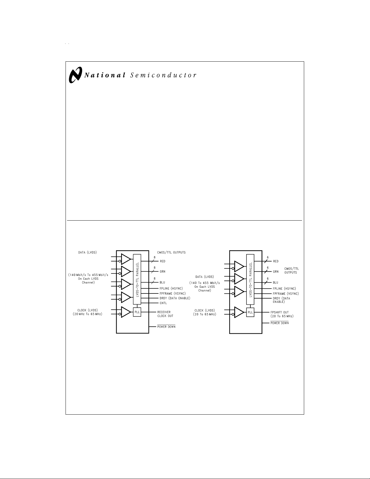
The DS90CF384A receiver converts the four LVDS data
streams (Up to 1.8 Gbps throughput or 227 Megabytes/sec
bandwidth) back into parallel 28 bits of CMOS/TTL data (24
bits of RGB and 4 bits of Hsync,Vsync, DE and CNTL).Also
available is the DS90CF364A that converts the three LVDS
data streams (Up to 1.3 Gbps throughput or 170 Megabytes/
sec bandwidth) back into parallel 21 bits of CMOS/TTL data
(18 bits of RGB and 3 bits of Hsync, Vsync and DE). Both
Receivers’ outputs are Falling edge strobe. A Rising edge or
Falling edge strobe transmitter (DS90C383A/DS90C363A)
will interoperate with a Falling edge strobe Receiver without
any translation logic.
This chipset is an ideal means to solve EMI and cable size
problems associated with wide, high speed TTL interfaces.
Block Diagrams
DS90CF384A
Features
n 20 to 65 MHz shift clock support
n 50%duty cycle on receiver output clock
n Best–in–Class Set & Hold Times on RxOUTPUTs
n Rx power consumption
Grayscale
n Rx Power-down mode
n ESD rating
n Supports VGA, SVGA, XGA and Dual Pixel SXGA.
n PLL requires no external components
n Compatible with TIA/EIA-644 LVDS standard
n Low profile 56-lead or 48-lead TSSOP package
>
7 kV (HBM),>700V (EIAJ)
<
250 mW (typ)@65MHz
<
200µW (max)
DS90CF364A
DS100870-27
Order Number DS90CF384AMTD
See NS Package Number MTD56
TRI-STATE®is a registered trademark of National Semiconductor Corporation.
© 1998 National Semiconductor Corporation DS100870 www.national.com
Order Number DS90CF364AMTD
See NS Package Number MTD48
DS100870-28
Page 2
Absolute Maximum Ratings (Note 1)
If Military/Aerospace specified devices are required,
please contact the National Semiconductor Sales Office/
Distributors for availability and specifications.
Supply Voltage (V
CMOS/TTL Output Voltage −0.3V to (V
LVDS Receiver Input Voltage −0.3V to (V
Junction Temperature +150˚C
Storage Temperature −65˚C to +150˚C
Lead Temperature
(Soldering, 4 sec) +260˚C
Maximum Package Power Dissipation Capacity
MTD56 (TSSOP) Package:
DS90CF384A 1.61 W
MTD48 (TSSOP) Package:
DS90CF364A 1.89 W
) −0.3V to +4V
CC
CC
CC
@
25˚C
+ 0.3V)
+ 0.3V)
Package Derating:
DS90CF384A 12.4 mW/˚C above +25˚C
DS90CF364A 15 mW/˚C above +25˚C
ESD Rating
(HBM, 1.5 kΩ, 100 pF)
(EIAJ, 0Ω, 200 pF)
>
>
Recommended Operating
Conditions
Supply Voltage (V
) 3.0 3.3 3.6 V
CC
Operating Free Air
Temperature (T
) −10 +25 +70 ˚C
A
Receiver Input Range 0 2.4 V
Supply Noise Voltage (V
Min Nom Max Units
) 100 mV
CC
7kV
700V
Electrical Characteristics
Over recommended operating supply and temperature ranges unless otherwise specified.
Symbol Parameter Conditions Min Typ Max Units
CMOS/TTL DC SPECIFICATIONS
V
OH
V
OL
I
OS
LVDS RECEIVER DC SPECIFICATIONS
V
TH
V
TL
I
IN
RECEIVER SUPPLY CURRENT
ICCRW Receiver Supply Current C
ICCRW Receiver Supply Current C
ICCRG Receiver Supply Current, C
ICCRZ Receiver Supply Current Power Down = Low
Note 1: “Absolute Maximum Ratings” are those values beyond which the safety of the device cannot be guaranteed. They are not meant to imply that the device
should be operated at these limits. The tables of “Electrical Characteristics” specify conditions for device operation.
Note 2: Typical values are given for V
Note 3: Current into device pins is defined as positive. Current out of device pins is defined as negative. Voltages are referenced to ground unless otherwise speci-
fied (except V
High Level Output Voltage IOH= −0.4 mA 2.7 3.3 V
Low Level Output Voltage IOL= 2 mA 0.06 0.3 V
Output Short Circuit Current V
= 0V −60 −120 mA
OUT
Differential Input High Threshold VCM= +1.2V +100 mV
Differential Input Low Threshold −100 mV
Input Current VIN= +2.4V, VCC= 3.6V
V
= 0V, VCC= 3.6V
IN
= 8 pF, f = 32.5 MHz 49 65 mA
L
±
10 µA
±
10 µA
Worst Case Worst Case Pattern, f = 37.5 MHz 53 70 mA
DS90CF384A
(Figures
f = 65 MHz 81 105 mA
1,4)
= 8 pF, f = 32.5 MHz 49 55 mA
L
Worst Case Worst Case Pattern, f = 37.5 MHz 53 60 mA
DS90CF364A
(Figures
f = 65 MHz 78 90 mA
1,4)
= 8 pF, f = 32.5 MHz 28 45 mA
L
16 Grayscale 16 Grayscale Pattern, f = 37.5 MHz 30 47 mA
(Figures 2, 3, 4 )
f = 65 MHz 43 60 mA
10 55 µA
Power Down Receiver Outputs Stay Low during
Power Down Mode
= 3.3V and TA= +25C.
CC
and ∆VOD).
OD
PP
www.national.com 2
Page 3
Receiver Switching Characteristics
Over recommended operating supply and temperature ranges unless otherwise specified
Symbol Parameter Min Typ Max Units
CLHT CMOS/TTL Low-to-High Transition Time
CHLT CMOS/TTL High-to-Low Transition Time
RSPos0 Receiver Input Strobe Position for Bit 0
,
Figure 12 )
11
(Figure 4 )
(Figure 4 )
(Figure
f = 65 MHz 0.7 1.1 1.4 ns
25ns
1.8 5 ns
RSPos1 Receiver Input Strobe Position for Bit 1 2.9 3.3 3.6 ns
RSPos2 Receiver Input Strobe Position for Bit 2 5.1 5.5 5.8 ns
RSPos3 Receiver Input Strobe Position for Bit 3 7.3 7.7 8.0 ns
RSPos4 Receiver Input Strobe Position for Bit 4 9.5 9.9 10.2 ns
RSPos5 Receiver Input Strobe Position for Bit 5 11.7 12.1 12.4 ns
RSPos6 Receiver Input Strobe Position for Bit 6 13.9 14.3 14.6 ns
RSKM RxIN Skew Margin (Note 4)
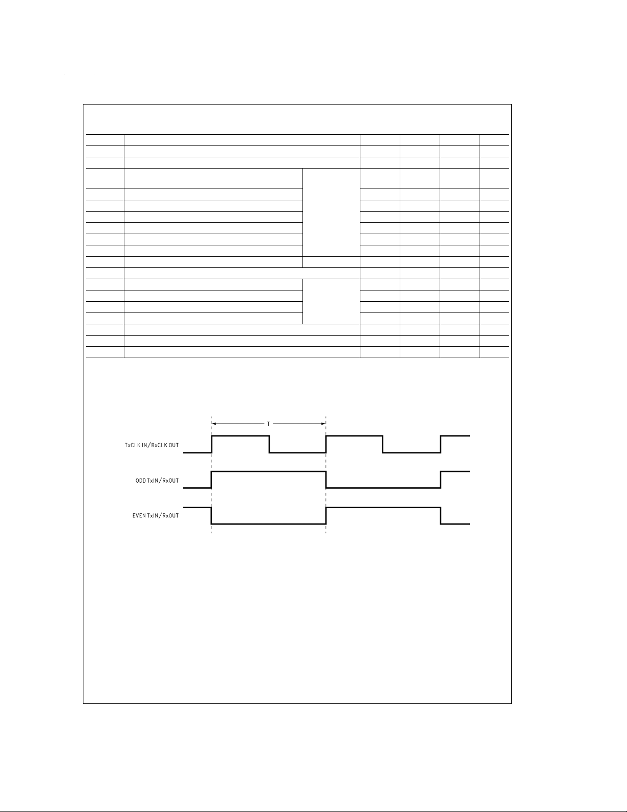
RCOP RxCLK OUT Period
RCOH RxCLK OUT High Time
RCOL RxCLK OUT Low Time
RSRC RxOUT Setup to RxCLK OUT
RHRC RxOUT Hold to RxCLK OUT
RCCD RxCLK IN to RxCLK OUT Delay 25˚C, V
RPLLS Receiver Phase Lock Loop Set
RPDD Receiver Power Down Delay
Note 4: ReceiverSkew Margin is defined as the validdatasampling region at the receiver inputs. Thismargintakes into account the transmitter pulse positions(min
and max) and the receiver input setup and hold time (internal data sampling window - RSPos). This margin allows for LVDS interconnect skew, inter-symbol interference (both dependent on type/length of cable), and clock jitter (less than 250 ps).
(Figure 5)
(Figure 5 )
(Figure 5)
(Figure 13 )
(Figure 5 )
(Figure 5 )
(Figure 7 )
(Figure 10 )
CC
= 3.3V
f = 65 MHz 400 ps
15 T 50 ns
f = 65 MHz 5.0 7.6 9.0 ns
5.0 6.3 9.0 ns
4.5 7.3 ns
4.0 6.3 ns
(Figure 6 )
3.5 5.0 7.5 ns
10 ms
1µs
AC Timing Diagrams
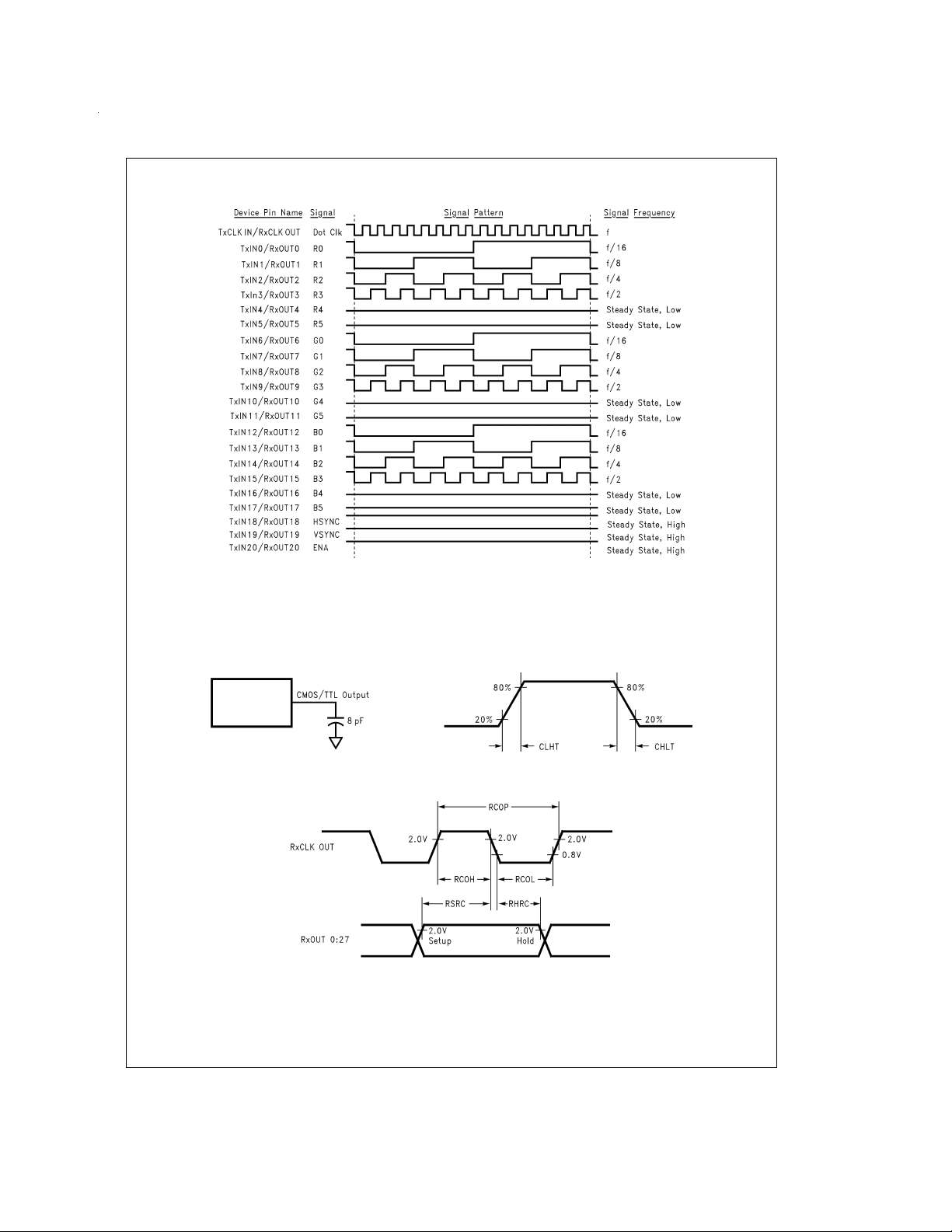
FIGURE 1. “Worst Case” Test Pattern
DS100870-2
www.national.com3
Page 4
AC Timing Diagrams (Continued)
FIGURE 2. “16 Grayscale” Test Pattern (DS90CF384A)(Notes 5, 6, 7, 8)
www.national.com 4
DS100870-12
Page 5
AC Timing Diagrams (Continued)
DS100870-3
FIGURE 3. “16 Grayscale” Test Pattern (DS90CF364A)(Notes 5, 6, 7, 8)
Note 5: The worst case test pattern produces a maximum toggling of digital circuits, LVDS I/O and CMOS/TTL I/O.
Note 6: The 16 grayscale test pattern tests device power consumption for a “typical” LCD display pattern. The test pattern approximates signal switching needed
to produce groups of 16 vertical stripes across the display.
Note 7:
Figures 1, 3
Note 8: Recommended pin to signal mapping. Customer may choose to define differently.
show a falling edge data strobe (TxCLK IN/RxCLK OUT).
DS100870-4
FIGURE 4. DS90CF384A/DS90CF364A (Receiver) CMOS/TTL Output Load and Transition Times
DS100870-5
FIGURE 5. DS90CF384A/DS90CF364A (Receiver) Setup/Hold and High/Low Times
www.national.com5
Page 6

AC Timing Diagrams (Continued)
FIGURE 6. DS90CF384A/DS90CF364A (Receiver) Clock In to Clock Out Delay
FIGURE 7. DS90CF384A/DS90CF364A (Receiver) Phase Lock Loop Set Time
DS100870-6
DS100870-7
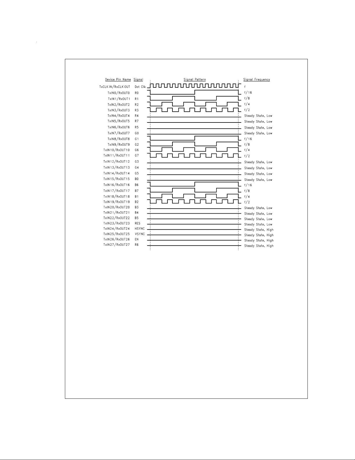
FIGURE 8. 28 Parallel TTL Data Inputs Mapped to LVDS Outputs - DS90CF384A
www.national.com 6
DS100870-9
Page 7

AC Timing Diagrams (Continued)
FIGURE 9. 21 Parallel TTL Data Inputs Mapped to LVDS Outputs - DS90CF364A
DS100870-10
FIGURE 10. DS90CF384A/DS90CF364A (Receiver) Power Down Delay
DS100870-8
www.national.com7
Page 8

AC Timing Diagrams (Continued)
FIGURE 11. DS90CF384A (Receiver) LVDS Input Strobe Position
www.national.com 8
DS100870-25
Page 9

AC Timing Diagrams (Continued)
FIGURE 12. DS90CF364A (Receiver) LVDS Input Strobe Position
DS100870-26
www.national.com9
Page 10

AC Timing Diagrams (Continued)
C—Setup and Hold Time (Internal data sampling window) defined by Rspos (receiver input strobe position) min and max
Tppos—Transmitter output pulse position (min and max)
RSKM = Cable Skew (type, length) + Source Clock Jitter (cycle to cycle) (Note 9) + ISI (Inter-symbol interference) (Note 10)
Cable Skew — typically 10 ps–40 ps per foot, media dependent
Note 9: Cycle-to-cycle jitter is less than 250 ps at 65 MHz.
Note 10: ISI is dependent on interconnect length; may be zero.
FIGURE 13. Receiver LVDS Input Skew Margin
DS100870-11
www.national.com 10
Page 11

DS90CF384A Pin Description—24-Bit FPD Link Receiver
Pin Name I/O No. Description
RxIN+ I 4 Positive LVDS differentiaI data inputs.
RxIN− I 4 Negative LVDS differential data inputs.
RxOUT O 28 TTL level data outputs. This includes: 8 Red, 8 Green, 8 Blue, and 3 control
lines—FPLINE, FPFRAME, DRDY (also referred to as HSYNC, VSYNC, Data
Enable).
RxCLK IN+ I 1 Positive LVDS differential clock input.
RxCLK IN− I 1 Negative LVDS differential clock input.
RxCLK OUT O 1 TTL Ievel clock output. The falling edge acts as data strobe.
PWR DOWN
V
CC
I 1 TTL level input. When asserted (low input) the receiver outputs are low.
I 4 Power supply pins for TTL outputs.
GND I 5 Ground pins for TTL outputs.
PLL V
CC
I 1 Power supply for PLL.
PLL GND I 2 Ground pin for PLL.
LVDS V
CC
I 1 Power supply pin for LVDS inputs.
LVDS GND I 3 Ground pins for LVDS inputs.
DS90CF364A Pin Description—18-Bit FPD Link Receiver
Pin Name I/O No. Description
RxIN+ I 3 Positive LVDS differentiaI data inputs. (Note 11)
RxIN− I 3 Negative LVDS differential data inputs. (Note 11)
RxOUT O 21 TTL level data outputs. This includes: 6 Red, 6 Green, 6 Blue, and 3 control lines— FPLINE,
RxCLK IN+ I 1 Positive LVDS differential clock input.
RxCLK IN− I 1 Negative LVDS differential clock input.
RxCLK OUT O 1 TTL Ievel clock output. The falling edge acts as data strobe.
PWR DOWN
V
CC
I 1 TTL level input. When asserted (low input) the receiver outputs are low.
I 4 Power supply pins for TTL outputs.
GND I 5 Ground pins for TTL outputs.
PLL V
CC
I 1 Power supply for PLL.
PLL GND I 2 Ground pin for PLL.
LVDS V
CC
I 1 Power supply pin for LVDS inputs.
LVDS GND I 3 Ground pins for LVDS inputs.
Note 11: These receivers have input failsafe bias circuitry to guarantee a stablereceiver output for floating orterminated receiver inputs. Under these conditions receiver inputs will be in a HIGH state. If a clock signal is present, outputs will all be HIGH; if the clock input is also floating/terminated outputs will remain in the last
valid state. A floating/terminated clock input will result in a HIGH clock output.
FPFRAME, DRDY (also referred to as HSYNC, VSYNC, Data Enable).
www.national.com11
Page 12

Pin Diagram
DS90CF384A
DS90CF364A
DS100870-13
DS100870-23
www.national.com 12
Page 13
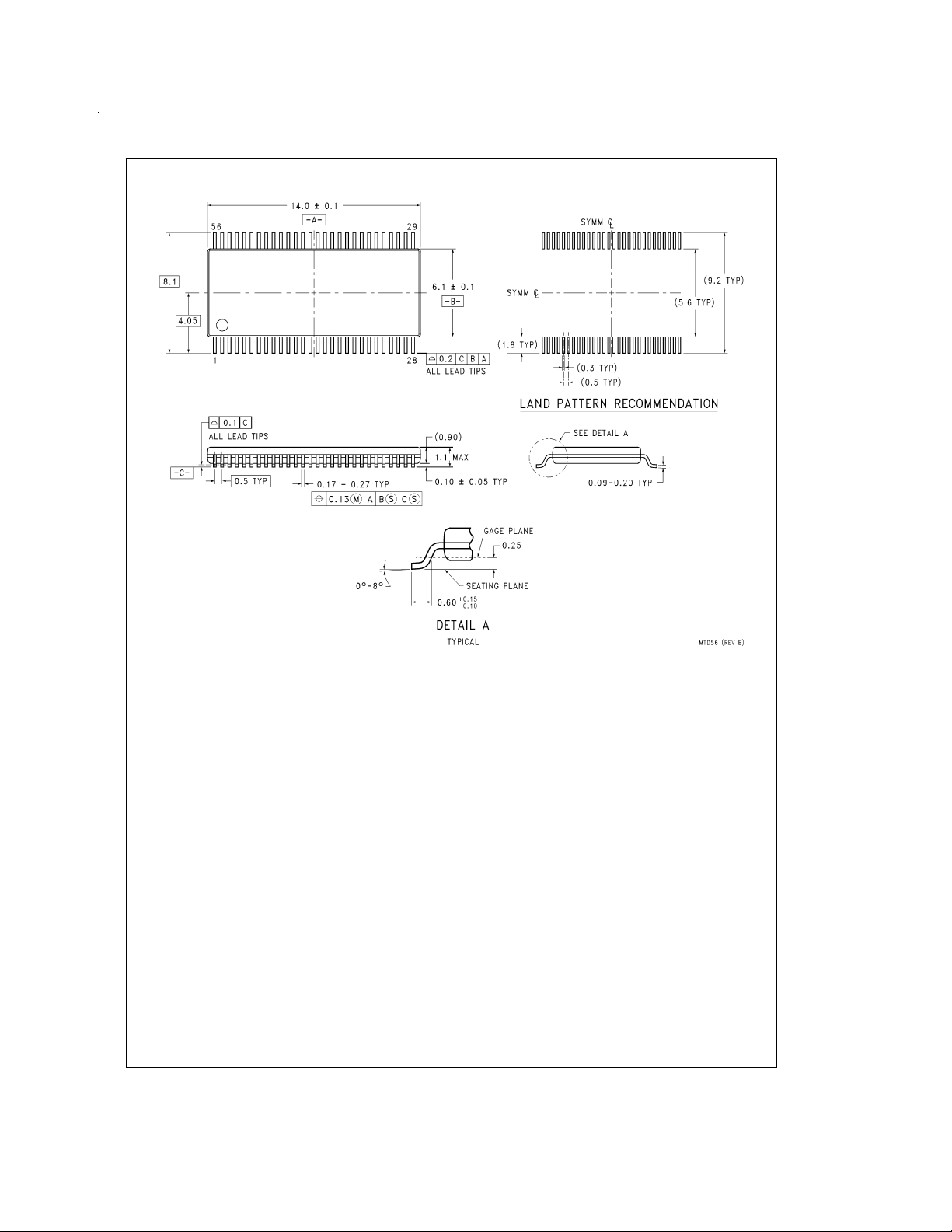
Physical Dimensions inches (millimeters) unless otherwise noted
56-Lead Molded Thin Shrink Small Outline Package, JEDEC
Order Number DS90CF384AMTD
NS Package Number MTD56
www.national.com13
Page 14

Physical Dimensions inches (millimeters) unless otherwise noted (Continued)
DS90CF384A/DS90CF364A +3.3V LVDS Receiver 24-Bit-Color Flat Panel Display (FPD)
Link— 65 MHz, +3.3V LVDS Receiver 18-Bit-Color Flat Panel Display (FPD) Link—65 MHz
48-Lead Molded Thin Shrink Small Outline Package, JEDEC
Order Number DS90CF364AMTD
NS Package Number MTD48
LIFE SUPPORT POLICY
NATIONAL’S PRODUCTS ARE NOT AUTHORIZED FOR USE AS CRITICAL COMPONENTS IN LIFE SUPPORT DEVICES OR SYSTEMS WITHOUT THE EXPRESS WRITTEN APPROVAL OF THE PRESIDENT OF NATIONAL SEMICONDUCTOR CORPORATION. As used herein:
1. Life support devices or systems are devices or systems which, (a) are intended for surgical implant into
the body, or (b) supportor sustainlife, and whose failure to perform when properly used in accordance
2. A critical component in any component of a life support
device or system whose failure to perform can be reasonably expected to causethe failure of the life support
device or system, or to affect itssafety oreffectiveness.
with instructions for use provided in the labeling, can
be reasonably expected to result in asignificant injury
to the user.
National Semiconductor
Corporation
Americas
Tel: 1-800-272-9959
Fax: 1-800-737-7018
Email: support@nsc.com
www.national.com
National Semiconductor
Europe
Fax: +49 (0) 1 80-530 85 86
Email: europe.support@nsc.com
Deutsch Tel: +49 (0) 1 80-530 85 85
English Tel: +49 (0) 1 80-532 78 32
Français Tel: +49 (0) 1 80-532 93 58
Italiano Tel: +49 (0) 1 80-534 16 80
National Semiconductor
Asia Pacific Customer
Response Group
Tel: 65-2544466
Fax: 65-2504466
Email: sea.support@nsc.com
National Semiconductor
Japan Ltd.
Tel: 81-3-5620-6175
Fax: 81-3-5620-6179
National does not assume any responsibility for use of any circuitry described, no circuit patent licenses are implied and National reserves the right at any time without notice to change said circuitry and specifications.
 Loading...