

查询DS90C365MTD供应商
DS90C385/DS90C365
+3.3V Programmable LVDS Transmitter 24-Bit Flat Panel
Display (FPD) Link-85 MHz, +3.3V Programmable LVDS
Transmitter 18-Bit Flat Panel Display (FPD) Link-85 MHz
General Description
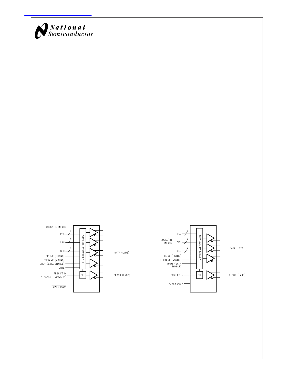
The DS90C385 transmitter converts 28 bits of LVCMOS/
LVTTL data into four LVDS (Low Voltage Differential Signaling) data streams. A phase-locked transmit clock is transmitted in parallel with the data streams over a fifth LVDS link.
Every cycle of the transmit clock 28 bits of input data are
sampled and transmitted. At a transmit clock frequency of 85
MHz, 24 bits of RGB data and 3 bits of LCD timing and
control data (FPLINE, FPFRAME, DRDY) are transmitted at
a rate of 595 Mbps per LVDS data channel. Using a 85 MHz
clock, the data throughput is 297.5 Mbytes/sec. Also available is the DS90C365 that converts 21 bits of LVCMOS/
LVTTL data into three LVDS (Low Voltage Differential Signaling) data streams. Both transmitters can be programmed
for Rising edge strobe or Falling edge strobe through a
dedicated pin. A Rising edge or Falling edge strobe transmitter will interoperate with a Falling edge strobe Receiver
(DS90CF386/DS90CF366) without any translation logic.
The DS90C385 is also offered in a 64 ball, 0.8mm fine pitch
ball grid array (FBGA) package which provides a 44 %
reduction in PCB footprint compared to the TSSOP package.
This chipset is an ideal means to solve EMI and cable size
problems associated with wide, high-speed TTL interfaces.
Features
n 20 to 85 MHz shift clock support
n Best–in–Class Set & Hold Times on TxINPUTs
<
n Tx power consumption
Grayscale
n Tx Power-down mode
n Supports VGA, SVGA, XGA and Dual Pixel SXGA.
n Narrow bus reduces cable size and cost
n Up to 2.38 Gbps throughput
n Up to 297.5 Megabytes/sec bandwidth
n 345 mV (typ) swing LVDS devices for low EMI
n PLL requires no external components
n Compatible with TIA/EIA-644 LVDS standard
n Low profile 56-lead or 48-lead TSSOP package
n DS90C385 also available in a 64 ball, 0.8mm fine pitch
ball grid array (FBGA) package
130 mW (typ)@85MHz
<
200µW (max)
May 2003
DS90C385/DS90C365 +3.3V Programmable LVDS Transmitter 24-Bit Flat Panel Display (FPD)
Link-85 MHz, +3.3V Programmable LVDS Transmitter 18-Bit Flat Panel Display (FPD) Link-85 MHz
Block Diagrams
DS90C385
Order Number DS90C385MTD or DS90C385SLC
See NS Package Number MTD56 or SLC64A
10086801
DS90C365
10086829
Order Number DS90C365MTD
See NS Package Number MTD48
TRI-STATE®is a registered trademark of National Semiconductor Corporation.
© 2003 National Semiconductor Corporation DS100868 www.national.com
Absolute Maximum Ratings (Note 1)
If Military/Aerospace specified devices are required,
please contact the National Semiconductor Sales Office/
Distributors for availability and specifications.
Supply Voltage (V
CMOS/TTL Input Voltage −0.5V to (V
LVDS Driver Output Voltage −0.3V to (V
DS90C385/DS90C365
LVDS Output Short Circuit
Duration Continuous
Junction Temperature +150˚C
) −0.3V to +4V
CC
CC
CC
+ 0.3V)
+ 0.3V)
DS90C385SLC 2.0 W
Package Derating:
DS90C385MTD 12.5 mW/˚C above +25˚C
Package Derating:
DS90C365MTD 16 mW/˚C above +25˚C
DS90C385SLC 10.2 mW/˚C above +25˚C
ESD Rating
(HBM, 1.5kΩ, 100pF)
(EIAJ, 0Ω, 200 pF)
Latch Up Tolerance
@
25˚C
>
Storage Temperature −65˚C to +150˚C
Lead Temperature
(Soldering, 4 sec) +260˚C
Solder reflow Temperature
(20 sec for FBGA) +220˚C
Maximum Package Power Dissipation Capacity
@
MTD56 (TSSOP) Package:
DS90C385MTD 1.63 W
MTD48 (TSSOP) Package:
DS90C365MTD 1.98 W
25˚C
Recommended Operating
Conditions
Min Nom Max Units
Supply Voltage (V
Operating Free Air
Temperature (T
Supply Noise Voltage (V
TxCLKIN frequency 20 85 MHz
) 3.0 3.3 3.6 V
CC
) −10 +25 +70 ˚C
A
) 100 mV
CC
SLC64 (FBGA) Package:
Electrical Characteristics
Over recommended operating supply and temperature ranges unless otherwise specified.
Symbol Parameter Conditions Min Typ Max Units
LVCMOS/LVTTL DC SPECIFICATIONS
V
IH
V
IL
V
CL
I
IN
LVDS DC SPECIFICATIONS
V
OD
∆V
OD
V
OS
∆V
OS
I
OS
I
OZ
TRANSMITTER SUPPLY CURRENT
ICCTW Transmitter Supply Current
ICCTG Transmitter Supply Current
High Level Input Voltage 2.0 V
CC
Low Level Input Voltage GND 0.8 V
Input Clamp Voltage ICL= −18 mA −0.79 −1.5 V
Input Current VIN= 0.4V, 2.5V or V
V
= GND −10 0 µA
IN
CC
+1.8 +10 µA
Differential Output Voltage RL= 100Ω 250 345 450 mV
Change in VODbetween
35 mV
complimentary output states
Offset Voltage (Note 4) 1.125 1.25 1.375 V
Change in VOSbetween
35 mV
complimentary output states
Output Short Circuit Current V
Output TRI-STATE®Current Power Down = 0V,
Worst Case
DS90C385
16 Grayscale
DS90C385
= 0V, RL= 100Ω −3.5 −5 mA
OUT
±
1
V
=0VorV
OUT
= 100Ω,
R
L
= 5 pF,
C
L
Worst Case Pattern
(Figures 1, 4 )
= 100Ω,
R
L
= 5 pF,
C
L
16 Grayscale Pattern
(Figures 2, 4 )
CC
f = 32.5 MHz 31 45 mA
f = 40 MHz 32 50 mA
f = 65 MHz 37 55 mA
f = 85 MHz 42 60 mA
f = 32.5 MHz 29 38 mA
f = 40 MHz 30 40 mA
f = 65 MHz 35 45 mA
f = 85 MHz 39 50 mA
±
10 µA
>
>
±
300mA
7kV
500V
PP
V
www.national.com 2
Electrical Characteristics (Continued)
Over recommended operating supply and temperature ranges unless otherwise specified.
Symbol Parameter Conditions Min Typ Max Units
TRANSMITTER SUPPLY CURRENT
ICCTW Transmitter Supply Current
Worst Case
DS90C365
ICCTG Transmitter Supply Current
16 Grayscale
DS90C365
ICCTZ Transmitter Supply Current
Power Down
Note 1: “Absolute Maximum Ratings” are those values beyond which the safety of the device cannot be guaranteed. They are not meant to imply that the device
should be operated at these limits. The tables of “Electrical Characteristics” specify conditions for device operation.
Note 2: Typical values are given for V
Note 3: Current into device pins is defined as positive. Current out of device pins is defined as negative. Voltages are referenced to ground unless otherwise
specified (except V
Note 4: V
OS
and ∆VOD).
OD
previously referred as VCM.
= 3.3V and TA= +25C.
CC
= 100Ω,
R
L
= 5 pF,
C
L
Worst Case Pattern
(Figures 1, 4 )
= 100Ω,
R
L
= 5 pF,
C
L
16 Grayscale Pattern
(Figures 3, 4 )
f = 32.5 MHz 28 42 mA
f = 40 MHz 29 47 mA
f = 65 MHz 34 52 mA
f = 85 MHz 39 57 mA
f = 32.5 MHz 26 35 mA
f = 40 MHz 27 37 mA
f = 65 MHz 32 42 mA
f = 85 MHz 36 47 mA
Power Down = Low
Driver Outputs in TRI-STATE under
Power Down Mode
10 55 µA
DS90C385/DS90C365
Recommended Transmitter Input Characteristics
Over recommended operating supply and temperature ranges unless otherwise specified
Symbol Parameter Min Typ Max Units
TCIT TxCLK IN Transition Time (Figure 6) 1.0 6.0 ns
TCIP TxCLK IN Period (Figure 7) 11.76 T 50 ns
TCIH TxCLK IN High Time (Figure 7) 0.35T 0.5T 0.65T ns
TCIL TxCLK IN Low Time (Figure 7) 0.35T 0.5T 0.65T ns
TXIT TxIN Transition Time 1.5 6.0 ns
Transmitter Switching Characteristics
Over recommended operating supply and temperature ranges unless otherwise specified
Symbol Parameter Min Typ Max Units
LLHT LVDS Low-to-High Transition Time (Figure 5) 0.75 1.5 ns
LHLT LVDS High-to-Low Transition Time (Figure 5) 0.75 1.5 ns
TPPos0 Transmitter Output Pulse Position for Bit 0 (Figures 13, 14)
(Note 5)
TPPos1 Transmitter Output Pulse Position for Bit 1 3.32 3.57 3.82 ns
TPPos2 Transmitter Output Pulse Position for Bit 2 6.89 7.14 7.39 ns
TPPos3 Transmitter Output Pulse Position for Bit 3 10.46 10.71 10.96 ns
TPPos4 Transmitter Output Pulse Position for Bit 4 14.04 14.29 14.54 ns
TPPos5 Transmitter Output Pulse Position for Bit 5 17.61 17.86 18.11 ns
TPPos6 Transmitter Output Pulse Position for Bit 6 21.18 21.43 21.68 ns
TPPos0 Transmitter Output Pulse Position for Bit 0 (Figures 13, 14)
(Note 5)
TPPos1 Transmitter Output Pulse Position for Bit 1 2.00 2.20 2.40 ns
TPPos2 Transmitter Output Pulse Position for Bit 2 4.20 4.40 4.60 ns
TPPos3 Transmitter Output Pulse Position for Bit 3 6.39 6.59 6.79 ns
TPPos4 Transmitter Output Pulse Position for Bit 4 8.59 8.79 8.99 ns
TPPos5 Transmitter Output Pulse Position for Bit 5 10.79 10.99 11.19 ns
TPPos6 Transmitter Output Pulse Position for Bit 6 12.99 13.19 13.39 ns
f = 40 MHz −0.25 0 0.25 ns
f = 65 MHz −0.20 0 0.20 ns
www.national.com3
Transmitter Switching Characteristics (Continued)
Over recommended operating supply and temperature ranges unless otherwise specified
Symbol Parameter Min Typ Max Units
TPPos0 Transmitter Output Pulse Position for Bit 0 (Figures 13, 14)
(Note 5)
TPPos1 Transmitter Output Pulse Position for Bit 1 1.48 1.68 1.88 ns
TPPos2 Transmitter Output Pulse Position for Bit 2 3.16 3.36 3.56 ns
DS90C385/DS90C365
TPPos3 Transmitter Output Pulse Position for Bit 3 4.84 5.04 5.24 ns
TPPos4 Transmitter Output Pulse Position for Bit 4 6.52 6.72 6.92 ns
TPPos5 Transmitter Output Pulse Position for Bit 5 8.20 8.40 8.60 ns
TPPos6 Transmitter Output Pulse Position for Bit 6 9.88 10.08 10.28 ns
TSTC TxIN Setup to TxCLK IN (Figure 7) 2.5 ns
THTC TxIN Hold to TxCLK IN (Figure 7) 0ns
TCCD TxCLK IN to TxCLK OUT Delay (Figure 8) T
TxCLK IN to TxCLK OUT Delay (Figure 8) 2.8 7.1 ns
TJCC Transmitter Jitter Cycle-to-Cycle (Figures 15, 16) (Note 6) f = 85 MHz 110 150 ps
TPLLS Transmitter Phase Lock Loop Set (Figure 9) 10 ms
TPDD Transmitter Power Down Delay (Figure 12) 100 ns
Note 5: The Minimum and Maximum Limits are based on statistical analysis of the device performance over process, voltage, and temperature ranges. This
parameter is functionality tested only on Automatic Test Equipment (ATE).
Note 6: The limits are based on bench characterization of the device’s jitter response over the power supply voltage range. Output clock jitter is measured with a
cycle-to-cycle jitter of +/−3ns applied to the input clock signal while data inputs are switching (See Figures 15 and 16). A jitter event of 3ns, represents worse case
jump in the clock edge from most graphics controller VGA chips currently available. This parameter is used when calculating system margin as described in AN-1059.
f = 85 MHz −0.20 0 0.20 ns
= 25˚C, VCC=
A
3.8 6.3 ns
3.3V
f = 65 MHz 210 230 ps
f = 40 MHz 350 370 ps
AC Timing Diagrams
10086804
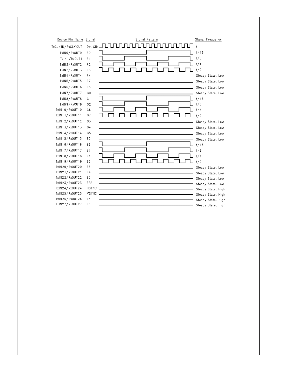
FIGURE 1. “Worst Case” Test Pattern (Note 7)
www.national.com 4
AC Timing Diagrams (Continued)
DS90C385/DS90C365
FIGURE 2. “16 Grayscale” Test Pattern - DS90C385 (Notes 8, 9, 10)
10086805
www.national.com5
AC Timing Diagrams (Continued)
DS90C385/DS90C365
10086831
FIGURE 3. “16 Grayscale” Test Pattern - DS90C365 (Notes 8, 9, 10)
Note 7: The worst case test pattern produces a maximum toggling of digital circuits, LVDS I/O and CMOS/TTL I/O.
Note 8: The 16 grayscale test pattern tests device power consumption for a “typical” LCD display pattern. The test pattern approximates signal switching needed
to produce groups of 16 vertical stripes across the display.
Note 9: Figures 1, 2 show a falling edge data strobe (TxCLK IN/RxCLK OUT).
Note 10: Recommended pin to signal mapping. Customer may choose to define differently.
10086830
FIGURE 4. DS90C385/DS90C365 (Transmitter) LVDS Output Load
10086806
FIGURE 5. DS90C385/DS90C365 (Transmitter) LVDS Transition Times
www.national.com 6

AC Timing Diagrams (Continued)
FIGURE 6. DS90C385/DS90C365 (Transmitter) Input Clock Transition Time
DS90C385/DS90C365
10086808
10086810
FIGURE 7. DS90C385/DS90C365 (Transmitter) Setup/Hold and High/Low Times (Falling Edge Strobe)
10086812
FIGURE 8. DS90C385/DS90C365 (Transmitter) Clock In to Clock Out Delay
FIGURE 9. DS90C385/DS90C365 (Transmitter) Phase Lock Loop Set Time
10086814
www.national.com7

AC Timing Diagrams (Continued)
DS90C385/DS90C365
FIGURE 10. 28 Parallel TTL Data Inputs Mapped to LVDS Outputs - DS90C385
10086817
FIGURE 11. 21 Parallel TTL Data Inputs Mapped to LVDS Outputs - DS90C365
FIGURE 12. Transmitter Power Down Delay
www.national.com 8
10086832
10086818

AC Timing Diagrams (Continued)
DS90C385/DS90C365
FIGURE 13. Transmitter LVDS Output Pulse Position Measurement - DS90C385
10086826
www.national.com9

AC Timing Diagrams (Continued)
DS90C385/DS90C365
FIGURE 14. Transmitter LVDS Output Pulse Position Measurement - DS90C365
FIGURE 15. TJCC Test Setup - DS90C385 Shown
10086833
10086827
www.national.com 10

AC Timing Diagrams (Continued)
FIGURE 16. Timing Diagram of the Input cycle-to-cycle clock jitter
DS90C385/DS90C365
10086828
DS90C385 MTD56 (TSSOP) Package Pin Description —
FPD Link Transmitter
Pin Name I/O No. Description
TxIN I 28 TTL level input. This includes: 8 Red, 8 Green, 8 Blue, and 4 control lines —FPLINE,
FPFRAME and DRDY (also referred to as HSYNC, VSYNC, Data Enable).
TxOUT+ O 4 Positive LVDS differentiaI data output.
TxOUT− O 4 Negative LVDS differential data output.
TxCLKIN I 1 TTL Ievel clock input. Pin name TxCLK IN.
R_FB I 1 Programmable strobe select (See Table 1).
TxCLK OUT+ O 1 Positive LVDS differential clock output.
TxCLK OUT− O 1 Negative LVDS differential clock output.
PWR DOWN
V
CC
GND I 4 Ground pins for TTL inputs.
PLL V
CC
PLL GND I 2 Ground pins for PLL.
LVDS V
LVDS GND I 3 Ground pins for LVDS outputs.
CC
I 1 TTL level input. Assertion (low input) TRI-STATES the outputs, ensuring low current at power
down. See Applications Information section.
I 3 Power supply pins for TTL inputs.
I 1 Power supply pin for PLL.
I 1 Power supply pin for LVDS outputs.
www.national.com11

DS90C385SLC SLC64A (FBGA) Package Pin Summary —
FPD Link Transmitter
Pin Name I/O No. Description
TxIN I 28 TTL level input.
TxOUT+ O 4 Positive LVDS differential data output.
TxOUT− O 4 Negative LVDS differential data output.
DS90C385/DS90C365
TxCLKIN I 1 TTL IeveI clock input. The rising edge acts as data strobe. Pin name TxCLK IN.
R_FB I 1 Programmable strobe select. HIGH = rising edge, LOW = falling edge.
TxCLK OUT+ O 1 Positive LVDS differential clock output.
TxCLK OUT− O 1 Negative LVDS differential clock output.
PWR DOWN
V
CC
GND I 5 Ground pins for TTL inputs.
PLL V
CC
PLL GND I 2 Ground pins for PLL.
LVDS V
LVDS GND I 4 Ground pins for LVDS outputs.
NC 6 Pins not connected.
CC
I 1 TTL level input. Assertion (low input) TRI-STATES the outputs, ensuring low current at
power down. See Applications Information section.
I 3 Power supply pins for TTL inputs.
I 1 Power supply pin for PLL.
I 2 Power supply pin for LVDS outputs.
DS90C385SLC SLC64A (FBGA) Package Pin Description —
FPD Link Transmitter
By Pin By Pin Type
Pin Pin Name Type Pin Pin Name Type
A1 TxIN27 I D3 GND G
A2 TxOUT0- O E4 GND G
A3 TxOUT0+ O E8 GND G
A4 LVDS VCC P G1 GND G
A5 LVDS VCC P G6 GND G
A6 TxCLKOUT- O B3 LVDS GND G
A7 TxCLKOUT+ O B4 LVDS GND G
A8 TxOUT3+ O B7 LVDS GND G
B1 TxIN1 I D5 LVDS GND G
B2 TxIN0 I C6 PLL GND G
B3 LVDS GND G D6 PLL GND G
B4 LVDS GND G D7 PWR DOWN
B5 TxOUT2- O G5 R_FB I
B6 TxOUT3- O C8 TxCLKIN I
B7 LVDS GND G B2 TxIN0 I
B8 NC B1 TxIN1 I
C1 TxIN3 I D2 TxIN2 I
C2 NC C1 TxIN3 I
C3 NC D1 TxIN4 I
C4 TxOUT1- O F1 TxIN5 I
C5 TxOUT2+ O E2 TxIN6 I
C6 PLL GND G E3 TxIN7 I
C7 PLL VCC P G2 TxIN8 I
C8 TxCLKIN I H1 TxIN9 I
D1 TxIN4 I G3 TxIN10 I
D2 TxIN2 I H3 TxIN11 I
D3 GND G F4 TxIN12 I
I
www.national.com 12

DS90C385SLC SLC64A (FBGA) Package Pin Description —
FPD Link Transmitter
By Pin By Pin Type
D4 TxOUT1+ O G4 TxIN13 I
D5 LVDS GND G H4 TxIN14 I
D6 PLL GND G H5 TxIN15 I
D7 PWD DOWN
D8 TxIN26 I F5 TxIN17 I
E1 VCC P H6 TxIN18 I
E2 TxIN6 I H7 TxIN19 I
E3 TxIN7 I H8 TxIN20 I
E4 GND G G7 TxIN21 I
E5 TxIN16 I F7 TxIN22 I
E6 VCC P G8 TxIN23 I
E7 TxIN24 I E7 TxIN24 I
E8 GND G F8 TxIN25 I
F1 TxIN5 I D8 TxIN26 I
F2 NC A1 TxIN27 I
F3 NC A6 TxCLKOUT- O
F4 TxIN12 I A7 TxCLKOUT+ O
F5 TxIN17 I A2 TxOUT0- O
F6 NC A3 TxOUT0+ O
F7 TxIN22 I C4 TxOUT1- O
F8 TxIN25 I D4 TxOUT1+ O
G1 GND G B5 TxOUT2- O
G2 TxIN8 I C5 TxOUT2+ O
G3 TxIN10 I B6 TxOUT3- O
G4 TxIN13 I A8 TxOUT3+ O
G5 R_FB I A4 LVDS VCC P
G6 GND G A5 LVDS VCC P
G7 TxIN21 I C7 PLL VCC P
G8 TxIN23 I E1 VCC P
H1 TxIN9 I E6 VCC P
H2 VCC P H2 VCC P
H3 TxIN11 I B8 NC
H4 TxIN14 I C2 NC
H5 TxIN15 I C3 NC
H6 TxIN18 I F2 NC
H7 TxIN19 I F3 NC
H8 TxIN20 I F6 NC
G : Ground
I : Input
O : Output
P : Power
NC : No Connect
(Continued)
I E5 TxIN16 I
DS90C385/DS90C365
www.national.com13

DS90C365 Pin Description —
FPD Link Transmitter
Pin Name I/O No. Description
TxIN I 21 TTL level input. This includes: 6 Red, 6 Green, 6 Blue, and 3 control lines —FPLINE,
FPFRAME and DRDY (also referred to as HSYNC, VSYNC, Data Enable).
TxOUT+ O 3 Positive LVDS differential data output.
DS90C385/DS90C365
TxOUT− O 3 Negative LVDS differential data output.
TxCLKIN I 1 TTL Ievel clock input. Pin name TxCLK IN.
R_FB I 1 Programmable strobe select (See Table 1).
TxCLK OUT+ O 1 Positive LVDS differential clock output.
TxCLK OUT− O 1 Negative LVDS differential clock output.
PWR DOWN
V
CC
GND I 4 Ground pins for TTL inputs.
PLL V
CC
PLL GND I 2 Ground pins for PLL.
LVDS V
LVDS GND I 3 Ground pins for LVDS outputs.
CC
I 1 TTL level input. Assertion (low input) TRI-STATES the outputs, ensuring low current at power
down. See Applications Information section.
I 3 Power supply pins for TTL inputs.
I 1 Power supply pin for PLL.
I 1 Power supply pin for LVDS outputs.
Applications Information
The DS90C385/DS90C365 are backward compatible with
the DS90C383/DS90C363, DS90C383A/DS90C363A and
the TSSOP versions are a pin-for-pin replacements. The
device (DS90C385/DS90C365) utilizes a different PLL architecture employing an internal 7X clock for enhanced pulse
position control.
This device (DS90C385/DS90C365) also features reduced
variation of the TCCD parameter which is important for dual
pixel applications. (See AN-1084) TCCD variation has been
measured to be less than 500ps at 85MHz under normal
operating conditions.
This device may also be used as a replacement for the
DS90CF583/563 (5V, 65MHz) and DS90CF581/561 (5V,
40MHz) FPD-Link Transmitters with certain considerations/
modifications:
1. Change 5V power supply to 3.3V. Provide this supply to
, LVDS VCCand PLL VCCof the transmitter.
the V
CC
2. The DS90C385/DS90C365 transmitter input and control
inputs accept 3.3V LVTTL/LVCMOS levels. They are not
5V tolerant.
3. To implement a falling edge device for the DS90C385/
DS90C365, the R_FB pin may be tied to ground OR left
unconnected (an internal pull-down resistor biases this
pin low). Biasing this pin to Vcc implements a rising edge
device.
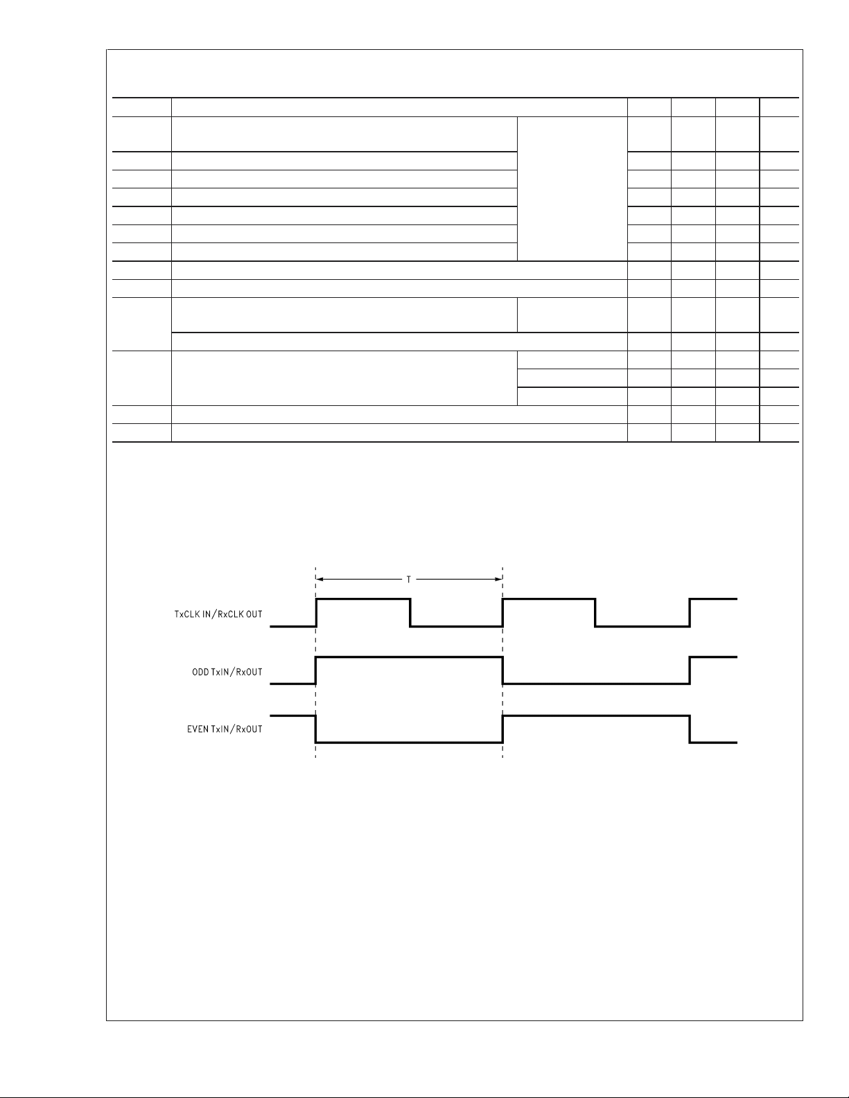
TRANSMITTER CLOCK JITTER CYCLE-TO-CYCLE
Figures 15 and 16 illustrate the timing of the input clock
relative to the input data. The input clock (TxCLKin) is intentionally shifted to the left −3ns and +3ns to the right when
data (Txin0-27) is high. This 3ns of cycle-to-cycle clock jitter
is repeated at a period of 2µs, which is the period of the input
data (1µs high, 1µs low). At different operating frequencies
the N Cycle is changed to maintain the desired 3ns cycleto-cycle jitter at 2µs period.
TRANSMITTER INPUT PINS
The TxIN and control input pins are compatible with LVCMOS and LVTTL levels. These pins are not 5V tolerant.
TRANSMITTER INPUT CLOCK
The transmitter input clock must always be present when the
device is enabled (PWR DOWN = HIGH). If the clock is
stopped, the PWR DOWN pin must be used to disable the
PLL. The PWR DOWN pin must be held low until after the
input clock signal has been reapplied. This will ensure a
proper device reset and PLL lock to occur.
POWER SEQUENCING AND POWERDOWN MODE
Outputs of the transmitter remain in TRI-STATE until the
power supply reaches 2V. Clock and data outputs will begin
to toggle 10 ms after V
down pin is above 1.5V. Either device may be placed into a
powerdown mode at any time by asserting the Powerdown
pin (active low). Total power dissipation for each device will
decrease to 5 µW (typical).
The transmitter input clock may be applied prior to powering
up and enabling the transmitter. The transmitter input clock
may also be applied after power up; however, the use of the
PWR DOWN pin is required as described in the Transmitter
Input Clock section. Do not power up and enable (PWR
DOWN = HIGH) the transmitter without a valid clock signal
applied to the TxCLK IN pin.
The FPD Link chipset is designed to protect itself from
accidental loss of power to either the transmitter or receiver.
If power to the transmit board is lost, the receiver clocks
(input and output) stop. The data outputs (RxOUT) retain the
states they were in when the clocks stopped. When the
receiver board loses power, the receiver inputs are controlled by a failsafe bias circuitry. The LVDS inputs are
High-Z during initial power on and power off conditions.
Current is limited (5 mA per input) by the fixed current mode
drivers, thus avoiding the potential for latchup when powering the device.
RECEIVER FAILSAFE FEATURE
The FPD Link receivers have input failsafe bias circuitry to
guarantee a stable receiver output for floating or terminated
receiver inputs. Under these conditions receiver inputs will
be pulled to a HIGH state. This is the case if not all data
channels are required in the application. Leave the extra
has reached 3V and the Power-
CC
www.national.com 14

Applications Information (Continued)
channel’s inputs open. This minimizes power dissipation and
locks the unused channels outputs into a stable known
(HIGH) state.
Pin Diagram for TSSOP Packages
DS90C385MTD DS90CF365MTD
DS90C385/DS90C365
If a clock signal is present, data outputs will all be HIGH; if
the clock input is also floating/terminated, data outputs will
remain in the last valid state. A floating/terminated clock
input will result in a LOW clock output.
10086823
Typical Application
TABLE 1. Programmable Transmitter (DS90C385/DS90C365)
Pin Condition Strobe Status
R_FB R_FB = V
CC
Rising edge strobe
R_FB R_FB = GND or NC Falling edge strobe
10086824
10086803
www.national.com15

Physical Dimensions inches (millimeters) unless otherwise noted
DS90C385/DS90C365
56-Lead Molded Thin Shrink Small Outline Package, JEDEC
Dimensions in millimeters only
Order Number DS90C385MTD
NS Package Number MTD56
48-Lead Molded Thin Shrink Small Outline Package, JEDEC
Dimensions in millimeters only
Order Number DS90C365MTD
NS Package Number MTD48
www.national.com 16

Physical Dimensions inches (millimeters) unless otherwise noted (Continued)
DS90C385/DS90C365 +3.3V Programmable LVDS Transmitter 24-Bit Flat Panel Display (FPD)
Link-85 MHz, +3.3V Programmable LVDS Transmitter 18-Bit Flat Panel Display (FPD) Link-85 MHz
64 ball, 0.8mm fine pitch ball grid array (FBGA) Package
Dimensions show in millimeters only
Order Number DS90C385SLC
NS Package Number SLC64A
LIFE SUPPORT POLICY
NATIONAL’S PRODUCTS ARE NOT AUTHORIZED FOR USE AS CRITICAL COMPONENTS IN LIFE SUPPORT
DEVICES OR SYSTEMS WITHOUT THE EXPRESS WRITTEN APPROVAL OF THE PRESIDENT AND GENERAL
COUNSEL OF NATIONAL SEMICONDUCTOR CORPORATION. As used herein:
1. Life support devices or systems are devices or
systems which, (a) are intended for surgical implant
into the body, or (b) support or sustain life, and
whose failure to perform when properly used in
accordance with instructions for use provided in the
2. A critical component is any component of a life
support device or system whose failure to perform
can be reasonably expected to cause the failure of
the life support device or system, or to affect its
safety or effectiveness.
labeling, can be reasonably expected to result in a
significant injury to the user.
National Semiconductor
Americas Customer
Support Center
Email: new.feedback@nsc.com
Tel: 1-800-272-9959
www.national.com
National does not assume any responsibility for use of any circuitry described, no circuit patent licenses are implied and National reserves the right at any time without notice to change said circuitry and specifications.
National Semiconductor
Europe Customer Support Center
Fax: +49 (0) 180-530 85 86
Email: europe.support@nsc.com
Deutsch Tel: +49 (0) 69 9508 6208
English Tel: +44 (0) 870 24 0 2171
Français Tel: +33 (0) 1 41 91 8790
National Semiconductor
Asia Pacific Customer
Support Center
Email: ap.support@nsc.com
National Semiconductor
Japan Customer Support Center
Fax: 81-3-5639-7507
Email: jpn.feedback@nsc.com
Tel: 81-3-5639-7560
 Loading...