

查询DS90C2501供应商
DS90C2501
Transmitter with built-in scaler for LVDS Display
Interface (LDI)
DS90C2501 Transmitter with built-in scaler for LVDS Display Interface (LDI)
October 2003
General Description
The DS90C2501 is a highly integrated scaling IC with LVDS
transmitter with a scaled resolution up to SXGA+ for single
pixel input. The DS90C2501 is a video controller hub designed to be compatible with Graphic Memory Controller
Hub (GMCH). The input interface can be single or dual DVO
port (12 pin per port). The high quality cubic zoom engine
scales the input graphics into the desired/optimal output
resolution up to 1400x1050 resolution. Advanced video digital signal processing provides gamma correction, and dithering for the display output. A two-wire serial interface is
used to communicate with the host system. The dual high
speed LVDS channels supports single pixel in-single pixel
out, single pixel in-dual pixel out, and dual pixel in-dual pixel
out transmission modes. The DS90C2501 complies to Open
LDI standard, and can be paired up with DS90CF388 receiver or FPD8531x/FPD8731x series integrated timing controller or FPDLink LVDS receivers such as DS90CF364/
DS90CF384A/DS90CF384/DS90CF384A. The LVDS output
is similar to DS90C387 and DS90C387R. Thus, this transmitter can be paired up with DS90CF388, receiver of
112MHz LDI chipset or FPD-Link Receivers in non-DC Balance mode operation which provides GUI/LCD panel/mother
board vendors a wide choice of inter-operation with LVDS
based TFT panels.
This chip is an ideal solution to solve EMI and cable size
problems for high-resolution flat panel applications. It provides a reliable industry standard interface based on LVDS
technology that delivers the bandwidth needed for highresolution panels while maximizing bit times, and keeping
clock rates low to reduce EMI and shielding requirements.
For more details, please refer to the “Applications Information” section of this datasheet.
Features
n Complies with Open LDI and GMCH DVO specification
for digital display interfaces
n 25 to 65 MHz clock in single pixel in to single pixel out
operation.
n 50 to 130 MHz clock in single pixel in to dual pixel out
operation.
n Support 24bit/48bit color TFT LCD with Conventional
and Non-Conventional Color Mappings.
n Support 16bit/32bit color TFT LCD.
n Single pixel transmitter inputs support single pixel GUI
interface.
n Up scaling/panel fitting supports VGA to SXGA+ output
in single pixel input mode at 640x480
800x600
1400x1050
n Independent horizontal and vertical scaling.
n Support dithering (available for 6-bit color only),
programmable smoothing and anti-aliasing filter.
n Programmable digital sharpness, edge enhancement
and contrast control via gamma correction.
n Allow 2% at 200KHz spread spectrum clocking, rejects
cycle-to-cycle jitter (+/− 20% of input data bit time).
n Programmable LCD panel power sequencing.
n Support low voltage swing signal level (1V to 1.8V),
2.5V and 3.3V LVTTL level on CLKINP, CLKINM, D0 to
D23, DE, HSYNC and VSYNC pins
n Support 2.5V/3.3V LVTTL level on configuration pins
n Support 3.3V LVTTL level on GPIO pins
n Available in 10mm x 10mm x 1mm 128pin thermally
enhanced CSP package.
n Two-wire serial communication interface is active during
normal as well as power down mode and support data
rates up to 400KHz.
n TIA/EIA-644, Open LDI, DVO compliance.
@
60Hz, 1024x768@60Hz, 1280x1024@60Hz,
@
60Hz.
@
60Hz,
TRI-STATE®is a registered trademark of National Semiconductor Corporation.
DVO is a registered trademark of Intel Corporation.
AGP or 4x AGP is a registered trademark of Intel Corporation.
© 2003 National Semiconductor Corporation DS200045 www.national.com
Block Diagram
DS90C2501
20004552
www.national.com 2
DS90C2501
Absolute Maximum Ratings (Note 1)
If Military/Aerospace specified devices are required,
please contact the National Semiconductor Sales Office/
Distributors for availability and specifications.
Supply Voltage (V
Supply Voltage (V
CMOS/TTL Input Voltage −0.3V to V
CMOS/TTL Output
Voltage −0.3V to (V
LVDS Driver Output
) −0.3V to +2.8V
CC
) −0.3V to +3.6V
CC3V
+ 0.3V)
CC
CC3V
Typical Package Power Dissipation Capacity
and Max V
CC
128 CSP Package:
DS90C2501 1.8W
Maximum Operating Case Temperature: 97˚C
(measured at top center of package)
ESD Rating:
DS90C2501
(HBM, 1.5kΩ, 100pF)
(EIAJ, 0Ω, 200pF)
@
>
>
70˚C
2kV
250 V
Voltage −0.3V to (VCC+ 0.3V)
LVDS Output Short
Circuit Duration Continuous
Junction Temperature +150˚C
Storage Temperature −65˚C to +150˚C
Lead Temperature
(Soldering, 4 sec.) +260˚C
Recommended Operating
Conditions
Min Nom Max Units
All Supply Voltage except
)
(V
CC3V
V
Supply Voltage 3.0 3.3 3.6 V
CC3V
2.250 2.5 2.750 V
Operating Free Air
Temperature (TA) 0 +25 +70 ˚C
Supply Noise Voltage (V
)
CC
100 mV
P-P
up to 33Mhz
DC Characteristics
Over recommended operating supply and temperature ranges unless otherwise specified.
Symbol Parameter Conditions Min Typ Max Units
LVCMOS/LVTTL DC SPECIFICATIONS (All input pins when operate in LVTTL level except DUAL pin. Note: On ID0, ID1
pins have typical 30K ohm internal pull-down, and ID2 and ID3 pins have typical 3K ohm internal pull-down.)
V
IH
V
IL
V
CL
I
IN
LVCMOS/LVTTL DC SPECIFICATIONS for DUAL pin, pin35
V
DUAL High Level Input Voltage (for
IH
DUAL High Level Input Voltage (for
V
IM
DUAL High Level Input Voltage (for
V
IL
V
CL
I
IN
LVCMOS/LVTTL DC SPECIFICATIONS for MSEN, pin 98
V
OL
LVCMOS/LVTTL DC SPECIFICATIONS (Pin 62 to pin 69 when operate in 3.3V LVTTL level)
V
OH
V
OL
I
OS
High Level Input Voltage V
Low Level Input Voltage V
REF=VCC3V
REF=VCC3V
2.0 V
CC3V
-0.3 0.8 V
Input Clamp Voltage ICL= 18 mA -0.9 -1.5 V
Input Current VIN= 0.4V, or V
V
= GND −15 0 µA
IN
PD=V
CC3V
CC
2.0 V
+1.8 +15 µA
CC
dual pixel in to dual pixel
out).
PD=V
CC3V
1
⁄2VCC−0.1
1
⁄2V
1
CC
⁄2VCC+0.1 V
single pixel in to dual pixel
out).
PD=V
CC3V
0 0.4 V
single pixel in to single pixel
out).
Input Clamp Voltage ICL= 18 mA -0.9 -1.5 V
Input Current VIN= 0.4V, V
V
= Gnd -15 0 µA
IN
Low level Open Drain Output
IOL= 2 mA 0.1 0.3 V
CC
1.8 15 µA
Voltage
High Level Input Voltage IOL= 2 mA 2.2 2.95 V
Low Level Input Voltage 0.055 0.4 V
Output Short Circuit Current V
= 0V -50 −120 mA
OUT
V
V
www.national.com3
DC Characteristics (Continued)
Over recommended operating supply and temperature ranges unless otherwise specified.
Symbol Parameter Conditions Min Typ Max Units
DS90C2501
Low Voltage Level DC SPECIFICATIONS (pins D0 to D23, CLKINP, CLKINM, DE, HSYNC,VSYNC)
V
DDQ
V
ILSH
V
ILSL
V
REF
LVDS DRIVER DC SPECIFICATIONS (Output pins AnP, AnM, CLKnP and CLKnM)
V
OD
∆V
OD
V
OS
∆V
OS
I
OS
I
OZ
SUPPLY CURRENT
I
1 Transmitter Supply Current
CC
2 Transmitter Supply Current
I
CC
3 Transmitter Supply Current
I
CC
4 Transmitter Supply Current
I
CC
ICCTZ Transmitter Supply Current
Low Swing Voltage from GMCH 1 +1.8 V
Low Swing High Level Input
Voltage
Low Swing Low Level Input
Voltage
Differential Input Reference
V
REF
+
V
DDQ
100mV
0V
REF
100mV
0.475
1
⁄2V
DDQ
0.945 V
Voltage
Differential Output Voltage RL= 100Ω 250 345 450 mV
Change in VODbetween
335mV
Complimentary Output
States
Offset Voltage 1.125 1.32 1.475 V
Change in VOSbetween
1.5 35 mV
Complimentary Output
States
Output Short Circuit Current V
Output TRI-STATE Current PD = 0V, V
when data input and clock
input are at Low Swing level.
when data input and clock
input are at Low Swing level.
when data input and clock
input are at Low Swing level.
= 0V 0 −8.5 -15 mA
OUT
OUT
= 100Ω,CL=
R
L
5 pF, DUAL pin
= GND, BAL =
GND, one 12bit
input, Pattern
Figure 1
= 100Ω,CL=
R
L
5 pF, DUAL pin
1
⁄2VCC, BAL =
=
GND, one 12bit
input, Pattern
Figure 1
= 100Ω,CL=
R
L
5 pF, DUAL pin
= GND, BAL =
=0VorV
CC
f = 65MHz,
scaler off, 2.75V
supply
f = 65 MHz,
scaler off, 3.6V
supply
f = 108MHz,
scaler off, 2.75V
supply
f = 108 MHz,
scaler off, 3.6V
supply.
f = 65 MHz,
scaler on, 2.75V
supply
±
0.1
70 120 mA
38 90 mA
85 130 mA
75 130 mA
330 415 mA
±
10 µA
GND, one 12bit
input
when data input and clock
input are at Low Swing level.
= 100Ω,CL=
R
L
5 pF, DUAL pin
1
⁄2VCC, BAL =
=
f = 108 MHz,
scaler on, 2.75V
supply
483 610 mA
GND, one 12bit
input
75 µA
Power Down
PD = GND. TST1, TST2, TST3, ID0,
ID1, ID2, ID3, A0, A1, A2, RES1,
RES2, RES3, RES4 = GND, BAL =
GND.
V
-
V
www.national.com 4
Two-Wire Serial Communication Interface
Unless otherwise noted, below specifications apply for VCC3V pin = 3.0V to 3.6V.
Symbol Parameter Conditions Min Typ Max Units
V
(1) Logical“1”input voltage 2.1 V
IN
V
(0) Logical“0”input voltage 0.8 V
IN
V
OL
Serial Bus Low level output
IOL= 3mA 0.1 0.4 V
voltage
= 6mA 0.15 0.6 V
I
OL
Recommended DVO Port Input Characteristics
Over recommended operating supply and temperature ranges unless otherwise specified.
Symbol Parameter Min Typ Max Units
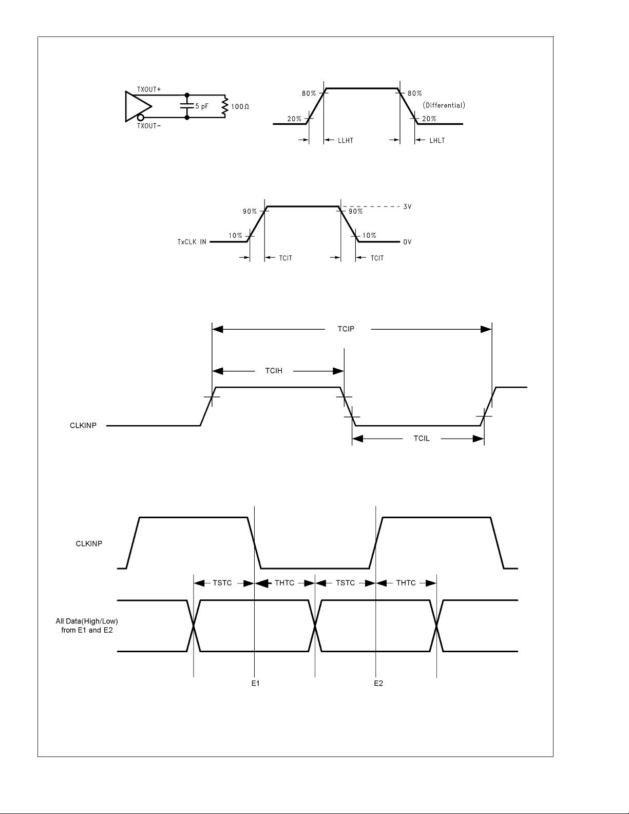
TCIT TxCLK IN Transition Time (Figure 4) DUAL = Gnd 0.8 1.2 2.4 ns
TCIP TxCLK IN Period (Figure 5) DUAL = Gnd 5.9 T 40 ns
TCIH TxCLK in High Time (Figure 5) 0.35T 0.5T 0.65T ns
TCIL TxCLK in Low Time (Figure 5) 0.35T 0.5T 0.65T ns
TXIT D0 to D23 Transition Time 1 ns
VDDQ Low Swing Voltage Amplitude from GMCH 1.0 1.8 V
DS90C2501
www.national.com5
AC Switching Characteristics
Over recommended operating supply and temperature ranges unless otherwise specified.
Symbol Parameter Min Typ Max Units
DS90C2501
LLHT LVDS Low-to-High Transition Time (Figure 3). (Note 7) 0.14 0.8 ns
LHLT LVDS High-to-Low Transition Time (Figure 3). (Note 7) 0.11 0.8 ns
TBIT Transmitter Output Bit Width DUAL pin = V
Gnd
DUAL pin =
TCCS TxOUT Channel to Channel Skew 100 ps
TPPOS0 Transmitter Output Pulse Position for Bit 0
(previous cycle) from CLK1P rising edge
f = 65 MHz, DUAL pin
=V
CC
(Note 7).
TPPOS1 Transmitter Output Pulse Position for Bit1
(previous cycle) from CLK1P rising edge.
f = 65 MHz, DUAL pin
=V
CC
(Note 7)
TPPOS2 Transmitter Output Pulse Position for Bit2
from CLK1P rising edge. (Note 7)
TPPOS3 Transmitter Output Pulse Position for Bit3
from CLK1P rising edge. (Note 7)
TPPOS4 Transmitter Output Pulse Position for Bit4
from CLK1P rising edge. (Note 7)
TPPOS5 Transmitter Output Pulse Position for Bit5
from CLK1P rising edge. (Note 7)
TPPOS6 Transmitter Output Pulse Position for Bit6
from CLK1P rising edge. (Note 7)
f = 65 MHz, DUAL pin
=V
CC
f = 65 MHz, DUAL pin
=V
CC
f = 65 MHz, DUAL pin
=V
CC
f = 65 MHz, DUAL pin
=V
CC
f = 65 MHz, DUAL pin
=V
CC
TSTC DxIN Setup to CLKINP (Figure 6) (Note 7) 0.8 ns
THTC DxIN Hold to CLKINP (Figure 6) (Note 7) 0.8 ns
TJCC Transmitter Jitter Cycle-to-cycle (Note 4) f = 85 MHz, DUAL pin
= Gnd
f = 54 MHz, DUAL pin
=V
CC
TPLLS Transmitter Phase Lock Loop Set (Figure 7) (Note 7) 10 ms
TPDD Transmitter Powerdown Delay (Figure 8) (Note 7) 100 ns
Transmitter Input to Output Latency for
f = 170 MHz (Note 6) 1.5 TCIP
single in-to-dual out mode. Figure 9
or
CC
1
⁄2V
CC
1/7 TCIP ns
2/7 TCIP ns
−0.49 0 +0.49 ns
(1/7)TCIP
−0.49
(2/7)TCIP
−0.49
(3/7)TCIP
−0.49
(4/7)TCIP
−0.49
(5/7)TCIP
−0.49
(6/7)TCIP
−0.49
(1/7)TCIP (1/7)TCIP
+0.49
(2/7)TCIP (2/7)TCIP
+0.49
(3/7)TCIP (3/7)TCIP
+0.49
(4/7)TCIP (4/7)TCIP
+0.49
(5/7)TCIP (5/7)TCIP
+0.49
(6/7)TCIP (6/7)TCIP
+0.49
114 ps
114 ps
+4.1
ns
ns
ns
ns
ns
ns
ns
www.national.com 6
Two-Wire Serial Communication Interface Switching Characteristics
Unless otherwise noted, below specifications apply for VCC3V pin = +3.3V, load capacitance on output lines = 80 pF. Load capacitance on output lines can be up to 400pF provided that external pull-up is on board. The following parameters are the timing relationship between SCL and SDA signals related to the DS90C2501.
Symbol Parameter Min Typ Max Units
t
1
t
2
t
3
t
4
t
5
Note 1: “Absolute Maximum Ratings” are those values beyond which the safety of the device cannot be guaranteed. They are not meant to imply that the device
should be operated at these limits. The tables of “Electrical Characteristics” specify conditions for device operation.
Note 2: Typical values are given for V
Note 3: Current into device pins is defined as positive. Current out of device pins is defined as negative. Voltages are referenced to ground unless otherwise
specified (except V
Note 4: The limits are based on bench characterization of the device’s jitter response over the power supply voltage range. Output clock jitter is measured with a
cycle-to-cycle jitter of
calculating system margin as described in AN-1059.
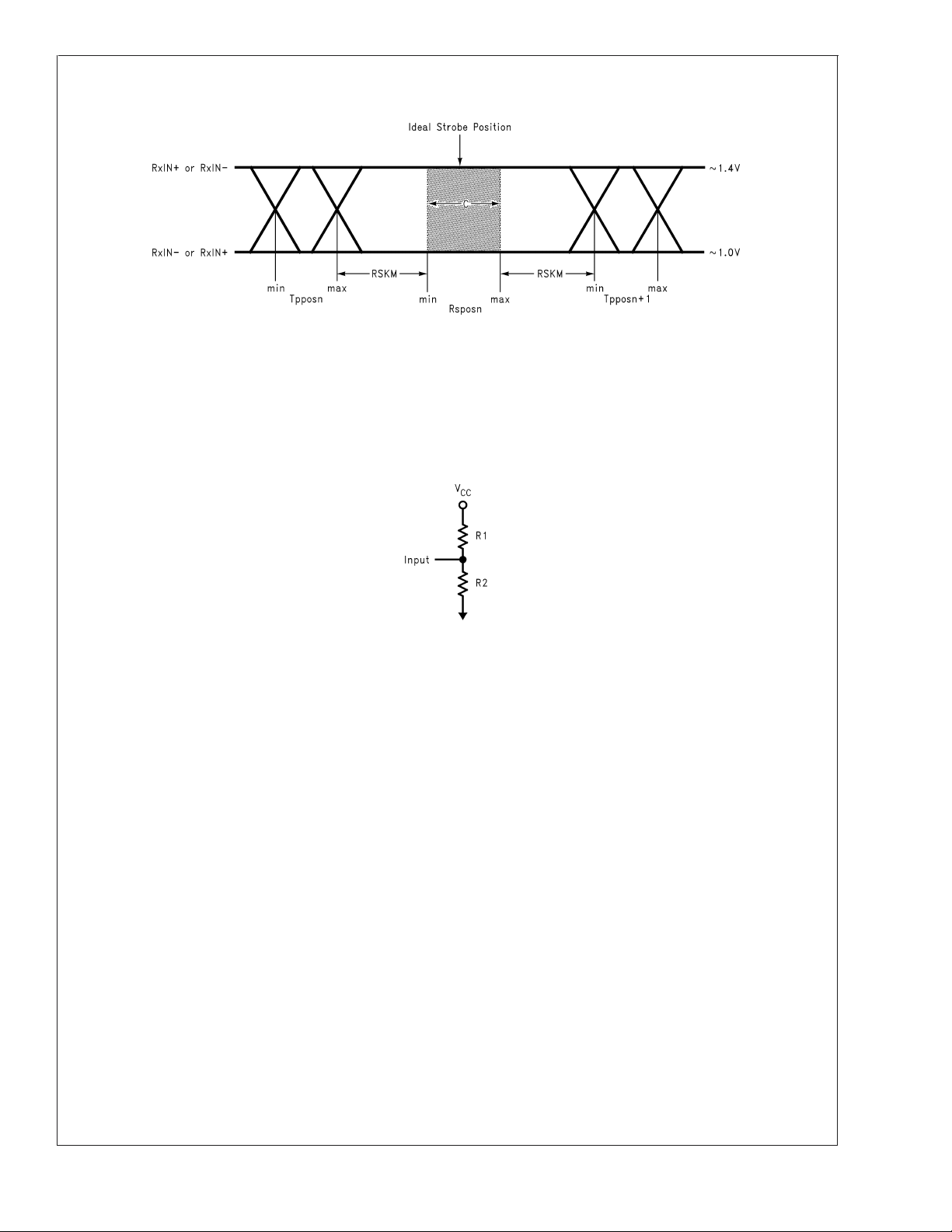
Note 5: Receiver Skew Margin is defined as the valid data sampling region at the receiver inputs. This margin takes into account transmitter output pulse positions
(min and max) and the receiver input setup and hold time (internal data sampling window - RSPOS). This margin allows for LVDS interconnect skew, inter-symbol
interference (both dependent on type/length of cable) and clock jitter.
RSKM ≥ cable skew (type, length) + source clock jitter (cycle to cycle).
Note 6: From V = 1.25V of CLKINP to V
Note 7: Guaranteed by Design
SCL (Clock) Period 2.5
Data in Set-Up Time to SCL High 100 ns
Data Out Stable after SCL Low 0 ns
SDA Low Set-Up Time to SCL Low (Start Condition) 100 ns
SDA High Hold Time after SCL High (Stop Condition) 100 ns
= 2.5V and V
CC
and ∆VOD).
OD
±
20% data input bit time applied to the input clock signal while data inputs are switching (see figures 11 and 12). This parameter is used when
= 0V of CLK1P when EDGE pin = Gnd, DUAL pin = Gnd or VCCor1⁄2VCC, BAL pin= Gnd.
DIFF
= 3.3V at TA= +25˚C.
CC3V
2000
(Note 7)
µs
DS90C2501
AC Timing Diagrams
FIGURE 1. “Alternate High/Low” Test Pattern in 12-bit Input Mode (Note 8)
20004532
www.national.com7
AC Timing Diagrams (Continued)
DS90C2501
20004551
FIGURE 2. “16 Grayscale” Test Pattern in 12-bit Input Mode(Note 9)
Note 8: The “Alternate High/Low” test pattern produces a maximum toggling of digital circuits, LVDS I/O and CMOS/TTL I/O.
Note 9: The 16 grayscale test pattern tests device power consumption for a “typical” LCD display pattern. The test pattern approximates signal switching needed
to produce groups of 16 vertical stripes across the display.
www.national.com 8
AC Timing Diagrams (Continued)
FIGURE 3. DS90C2501 (Transmitter) LVDS Output Load and Transition Times
FIGURE 4. DS90C2501 (Transmitter) Input Clock Transition Time
DS90C2501
20004512
20004514
FIGURE 5. DS90C2501 (Transmitter) Input Clock High/Low Times
FIGURE 6. Setup/Hold Times, V
20004554
= 0.900V, EDGE = Gnd, DUAL = VCC, BAL = Gnd
REF
20004555
www.national.com9
AC Timing Diagrams (Continued)
DS90C2501
FIGURE 7. DS90C2501 (Transmitter) Phase Lock Loop Set Time
20004519
FIGURE 8. Transmitter Power Down Delay
FIGURE 9. Transmitter Input to Output Lantency
20004521
20004553
www.national.com 10
AC Timing Diagrams (Continued)
DS90C2501
C —Setup and Hold Time (Internal data sampling window) defined by Rspos (receiver input strobe position) min and max
Tppos —Transmitter output pulse position (min and max)
RSKM = Cable Skew (type, length) + Source Clock Jitter (cycle to cycle) + ISI (Inter-symbol interference) (Note 10)
Cable Skew — typically 10 ps– 40 ps per foot, media dependent
Note 10: ISI is dependent on interconnect length; may be zero
20004525
FIGURE 10. Receiver Skew Margin
20004508
FIGURE 11. Resistor Network for “DUAL” pin input - recommend using R1=R2=10kΩ±1% for single to dual mode
www.national.com11
DS90C2501 Pin Description
Pin Name Pin No. I/O Type Description
DVO INTERFACE
DS90C2501
D0–D23 17, 16,
15, 14,
13, 12, 9,
8, 7, 6, 5,
4, 32, 31,
30, 29,
28, 27,
26, 25,
I-LVTTL/ Low
Swing (See
signal
V
REF
description
for more
information
on Low
Swing)
24, 23,
22, 21
DE 3 I-LVTTL/ Low
Swing
HSYNC 2 I-LVTTL/ Low
Swing
VSYNC 1 I-LVTTL/ Low
Swing
CLKINP 10 I-LVTTL/ Low
Swing
Differential
CLKINM 11 I-LVTTL/ Low
Swing
Differential
HOST INTERFACE
RESETN
61 I-LVTTL 2.5 Active low RESET signal. Asserting RESETN will reset all internal logic and
S2CCLK 72 I-LVTTL3V This is the clock line for the two-wire serial communication interface. Normally
S2CDAT 71 I/O-LVTTL3V This is the data line for two-wire serial communication interface. A Pull-up
MSEN 98 O-LVTTL 2.5 Interrupt signal. This is an open drain output, a pull-up resistor is required.
PD
99 I-LVTTL 2.5 Power Down Signal. A logic “0” will place the device in power down mode per
CLOCK
REFCLK1 18 I-LVTTL3V Reference clock, — A 3V, 14.318 MHz clock is required for internal control
DVO Port RGB input data
When DUAL pin = GND inputs D0–D11 correspond to LVDS ports A0–A3.
1
When DUAL pin =
⁄2VCC, 1st pixel from D0– D11 corresponds to LVDS ports
A0–A3, 2nd pixel from D0– D11 corresponds to LVDS ports A4–A7.
When DUAL pin = V
, 1st pixel from D0– D11 corresponds to LVDS ports
CC
A0–A3, 2nd pixel from D12– D23 corresponds to LVDS ports A4–A7.
Note: Ports refer to the corresponding differential LVDS pin pairs. The port A nomenclature should not
be confused with the serial interface slave address pins AO-A2.
Display Data Enable. When High, input pixel data is valid to DS90C2501
when R_FDE bit = High (default). See RFDE register field for more
information .
Display Horizontal Sync input control signal.
Display Vertical Sync input control signal.
“Positive” differential pixel clock input. A differential clock is recommended for
applications 65 MHz or higher.
“Minus” differential pixel clock input. A differential clock is recommended for
applications 65 MHz or higher.
clear the Host Interface registers.
a pull-up resistor is required in the system.
resistor is normally required in the system.
Please refer to MDI, RSEN, TSEL and MSEL register fields in Register Field
Definitions for more information. This signal requires support from host
software.
Table 1 below.
When maximum power savings is desired, the PD pin or soft power down bit
(Reg 08h bit 0) should be used to power down the DS90C2501.
LVDS outputs of the device will be in TRI-STATE.
Scaling engine will be powered down, and retain all register values.
PLL will be powered down.
All data input pads will be powered down. V
circuit is powered down. The
REF
two-wire serial communication interface remains active and all register
contents will be retained.
All GPIO pins will be disabled (tri-state if programmed as an output).
ENAVDD, ENABKL, PWM, VSTALL and HIRQ pins remain active and can be
accessed through the two-wire serial communication interface.
and timing. This clock must be stable when the DS90C2501 is powered-up.
www.national.com 12
DS90C2501 Pin Description (Continued)
Pin Name Pin No. I/O Type Description
OPTION SELECTION
BAL 97 I-LVTTL 2.5 Tie this pin to GND.
DUAL 35 I-LVTTL 2.5 LVTTL level input.
Input = GND for single pixel in-to-single pixel out mode. LVDS output
channels A0 to A3 are enabled, A4 to A7 are CLK2 are disable.
Input = V
to A7, CLK1 and CLK2 are enable. Use a 10K typ. pull-up resistor.
Input =
A0 to A7, CLK1 and CLK2 are enabled. See register CFG1 (08h) BPASS field
for more information.
See Figure 11 for example interface circuit.
COLOR 34 I-LVTTL 2.5 LVTTL level input to select RGB to LVDS color mapping.
Tie to GND for 18-bit/36-bit LCD.
Tie to GND to select conventional color mapping for 24-bit/48-bit LCD.
Tie to Logic “1” to select non-conventional color mapping for 24-bit/48-bit
LCD.
A0, A1, A2 115, 116,
117
I-LVTTL 2.5 These are input pins to select the 2-wire Serial Communication Slave Device
Address Lower Bits.
EDGE 36 I-LVTTL 2.5 Selects primary clock edge E1.
Tie to Logic “1” to select Rising edge for E1.
Tie to ground to select Falling edge for E1.
PANEL INTERFACE
A0P, A1P,
A2P, A3P
55, 53,
51, 47
O-LVDS Positive LVDS differential data output.
When DUAL pin = GND, input to D0–D11 will be coming out of A0P to A3P.
For 6-bit color application, no connect for channel A3P.
When DUAL pin =
of A0P to A3P, and the second pixel going in D0–D11 will come out of A4P to
A7P. For 6-bit color application, no connect for channels A3P and A7P.
When DUAL pin = V
A0P to A3P, the second pixel going in D12–D23 will be coming out of A4P to
A7P. For 6-bit color application, no connect for channels A3P and A7P.
A0M, A1M,
A2M, A3M
56, 54,
52, 48
O-LVDS Negative LVDS differential data output.
When DUAL pin = GND, input to D0–D11 will be coming out of A0M to A3M.
For 6-bit color application, no connect for channel A3M.
When DUAL pin =
of A0M to A3M, and the second pixel going in D0–D11 will come out of A4M
to A7M. For 6-bit color application, no connect for channels A3M and A7M.
When DUAL pin = V
A0M to A3M, the second pixel going in D12–D23 will be coming out of A4M
to A7M. For 6-bit color application, no connect for channels A3M and A7M.
A4P, A5P,
A6P, A7P
45, 43,
41, 39
O-LVDS Positive LVDS differential data output for second pixel.
When DUAL pin = GND, input to D0–D11 will be coming out of A0P to A3P.
For 6-bit color application, no connect for channel A3P.
When DUAL pin =
of A0P to A3P, and the second pixel going in D0–D11 will come out of A4P to
A7P. For 6-bit color application, no connect for channels A3P and A7P.
When DUAL pin = V
A0P to A3P, the second pixel going in D12–D23 will be coming out of A4P to
A7P. For 6-bit color application, no connect for channels A3P and A7P.
for dual pixel in-to-dual pixel out mode. LVDS output channel A0
CC
1
⁄2VCCfor single pixel in-to-dual pixel out mode. LVDS output channel
1
⁄2VCC, the first pixel going in D0–D11 will be coming out
, the first pixel going in D0–D11 will be coming out of
CC
1
⁄2VCC, the first pixel going in D0–D11 will be coming out
, the first pixel going in D0–D11 will be coming out of
CC
1
⁄2VCC, the first pixel going in D0–D11 will be coming out
, the first pixel going in D0–D11 will be coming out of
CC
DS90C2501
www.national.com13
DS90C2501 Pin Description (Continued)
Pin Name Pin No. I/O Type Description
OPTION SELECTION
DS90C2501
A4M, A5M,
A6M, A7M
CLK1P 49 O-LVDS Positive LVDS differential clock output.
CLK1M 50 O-LVDS Negative LVDS differential clock output.
CLK2P 37 O-LVDS Additional positive LVDS differential clock output pin. Identical to CLK1P. No
CLK2M 38 O-LVDS Additional negative LVDS differential clock output pin. Identical to CLK1M. No
ID0, ID1, ID2,
ID3
ENAVDD 69 O-LVTTL 2.5 Output to control LCD panel power under software control. Typically, this
ENABKL 68 O-LVTTL 2.5 Output to control LCD panel back light power under software control.
MISCELLANEOUS/TEST
GPIO1,
GPIO2,
GPIO3
CLK_INV 114 I-LVTTL 2.5 This pin is used to invert the polarity of the incoming pixel CLK
RES2 70 I-LVTTL 2.5 This pin is used in production testing and should be tied to GND in normal
RES3 113 I-LVTTL 2.5 This pin is used in production testing and should be tied to GND in normal
RES4 100 I-LVTTL 2.5 This pin is used in production testing and should be tied to GND in normal
PWM 67 O-LVTTL 3V This signal was provided for legacy support and is no longer required. This
VSTALL 66 O-LVTTL 3V This signal was provided for legacy support and is no longer required. This
HIRQ 65 O-LVTTL 3V This signal was provided for legacy support and is no longer required. This
46, 44,
42, 40
O-LVDS Negative LVDS differential data output for second pixel.
When DUAL pin = GND, input to D0–D11 will be coming out of A0M to A3M.
For 6-bit color application, no connect for channel A3M.
1
When DUAL pin =
⁄2VCC, the first pixel going in D0–D11 will be coming out
of A0M to A3M, and the second pixel going in D0–D11 will come out of A4M
to A7M. For 6-bit color application, no connect for channels A3M and A7M.
When DUAL pin = V
, the first pixel going in D0–D11 will be coming out of
CC
A0M to A3M, the second pixel going in D12–D23 will be coming out of A4M
to A7M. For 6-bit color application, no connect for channels A3M and A7M.
connect if not used.
connect if not used.
57, 58,
59, 60
I-LVTTL 2.5 These four pins are used to select one out of 16 pre-determined LCD display
timing information. The values are from 0 to 15. This function requires support
from VBIOS or display driver. Tie these pins to GND when not in use. Tie
these four pins [ID3, ID2, ID1, ID0] to High or Low for selecting LCD panel.
ID0 is the LSB, and ID3 is the MSB. For example: 1000 will select the 9th
LCD panel.
A 4-bit register field [3:0] will be used to store the selected value for the host
to read. See PANEL field for more information.
output is used with a power switch such as a FET circuit to control LCD panel
(Note 11).
V
CC
Typically, this output is used to control the enable on a backlight inverter
(Note 11).
64, 63, 62 I/O-LVTTL 3V General purpose inputs or outputs referenced to GND.
When the device is powered up, this pin defaults to an input.
When the scaler is in the power down state these signals are tri-state if
programmed as outputs (Note 11).
(CLKINP/CLKINM). A logic 0 = Normal, Logic 1 = Invert.
operation.
operation.
operation.
pin should be left open in normal operation.
pin should be left open in normal operation.
pin should be left open in normal operation.
www.national.com 14
DS90C2501 Pin Description (Continued)
Pin Name Pin No. I/O Type Description
OPTION SELECTION
V
REF
TST1, TST2,
TST3
POWER (See Application Information for power supply decoupling requirements)
V
/DV
CC
CC
GND/DGND 33, 73,
3V 121, 127 PWR The VCC3V is required for internal logic and certain 3V I/O.
V
CC
GND3V 120, 126,
SPLLV
CC
SPLLGND 86, 88, 90 PWR Ground returns for scaler PLL circuitry.
PLLV
CC
PLLGND 91, 93, 95 PWR Ground returns for Tx PLL circuitry.
LVDSV
CC
LVDSGND 104, 108 PWR Ground return pins for LVDS output drivers.
LVDSV
3V 101, 103,
CC
LVDSGND3V 102, 106,
Note 11: When device power is applied, it is possible for these outputs to switch to a logic “1” momentarily as the 3.3V is rising and before 2.5V reaches at least
0.8V. During this brief period, the pad control logic could be non-deterministic, RESETN will have no effect. It is recommended these outputs are gated externally
if the system design requires them to remain in the inactive logic “0” state during power-on.
83 I-ANALOG This pin is never to be left floating and never tie to GND.
For LVTTL level data input, tie V
to VCC3V. When V
REF
>
1.8V, input data
REF
is set to LVTTL level.
For low voltage swing level data input, tie V
host interface) V
is from the host. When V
DDQ
REF
to1⁄2V
DDQ(VDDQ
<
=1.0V, indicates input
REF
provided by
data is in low voltage swing mode.
Input data = logic High = V
Input data = logic Low = V
+100 mV in low voltage swing level.
REF
−100 mV in low voltage swing level.
REF
19, 20, 85 I-LVTTL 2.5 These pins are used in production testing and should be tied to GND in
normal operation.
81, 82,
75, 77,
PWR Power supply pins (pin 75, 77, 81, 82, 96, 119, 123, and 125) for 2.5V LVTTL
inputs and digital circuitry.
96, 119,
123, 125
PWR GND or DGND reference for 2.5V TTL inputs and digital circuitry.
74, 76,
78, 79,
80, 84,
118, 122,
124
During power up stage, voltage readings on these pins must be higher than
2.5V pins.
PWR Ground return pins for V
3V powered logic.
CC
128
87, 89 PWR 2.5V power supply pins for scaler PLL circuitry. It is not recommended to
share this power with PLLV
.
CC
92, 94 PWR 2.5V power supply pins for Tx PLL circuitry. It is not recommended to share
this power with SPLLV
.
CC
105, 109 PWR Power supply pins for LVDS output drivers.
PWR 3V power supply pins for LVDS output drivers.
107, 111
During power up stage, voltage readings on these pins must be higher than
2.5V pins.
PWR Ground return pins for 3V LVDS outputs.
110, 112
DS90C2501
www.national.com15

DS90C2501 Pin Description (Continued)
TABLE 1. scaler is powered down under these conditions
DS90C2501
/PD pin H L
DUAL pin
provided that PD
bit is 1 and
BYPASS bit is 0
No input clock is
detected
PD bit issued by
host
BYPASS bit
issued by host.
scaler is On scaler is OFF
1
⁄2V
Lor
CC
NO YES
10
01
Lor1⁄2VCCor VCC
Two-Wire Serial Communication
Interface Description
There are two register sets on DS90C2501. One set is for
controlling the input and output blocks as shown below, and
one set is for controlling the scaler which is not shown on this
datasheet. Both register sets are accessible by the host
system through the Two-Wire Serial Communication Interface. The DS90C2501 operates as a slave on the Serial Bus,
so the SCL line is an input (no clock is generated by the
DS90C2501) and the SDA line is bi-directional. DS90C2501
has a 7-bit slave address. The address bits are controlled by
the state of the address select pins A2, A1 and A0, and are
set by connecting these pins to ground for a LOW, (0) , to
3V pin for a HIGH, (1).
V
CC
Therefore, the complete slave address is:
A6 A5 A4 A3 A2 A1 A0
MSB LSB
and is selected as follows:
Address Select Pin
State
A2 A1 A0 A6:A0 binary
0 0 0 0111000
0 0 1 0111001
0 1 0 0111010
0 1 1 0111011
1 0 0 0 111100
1 0 1 0 111101
1 1 0 011111 0
1 1 1 0111111
DS90C2501 Serial
Bus Slave Address
(A6:A3 are hardwired
to "0111")
The DS90C2501 latches the state of the address select pins
during the first read or write on the Serial Bus. Changing the
state of the address select pins after the first read or write to
any device on the Serial Bus will not change the slave
address of the DS90C2501.
Communicating with the DS90C2501 Control Registers
All registers are predefined as read only, or read and write.
The Serial Interface will always attempt to detect if a LCD
panel/monitor is connected.
A Write to the DS90C2501 will always include the slave
address byte, data register address byte, a data byte.
A Read from the DS90C2501 can take place either of two
ways:
1. If the location latched in the data register addresses is
correct , then the read can simply consist of a slave
address byte, followed by retrieving the data byte.
2. If the data register address needs to be set, then a slave
address byte, data register address will be sent first,
then the master will repeat start, send the slave address
byte and receive data byte to accomplish a read.
The data byte has the most significant bit first. At the end of
a read, the DS90C2501 can accept either Acknowledge or
No Acknowledge from the Master (No Acknowledge is typically used as a signal for the slave that the Master has read
its last byte).
Serial Bus Protocol
The DS90C2501 slave state machine does not require an
internal clock, and supports only byte read and write. Page
mode is not supported. The 7-bit binary address is
“0 111A
A6:A3 are hardwired internally to "0111"
”, where A2A1A0are pin programmable and
2A1A0
www.national.com 16

Serial Bus Protocol (Continued)
DS90C2501
20004530
FIGURE 12. Byte Read
The master must generate a “ Start ”, and send the 7-bit
slave address plus a 0 first, and wait for acknowledge from
DS90C2501. When DS90C2501 acknowledges (the 1st
ACK) that the master is calling, the master then sends the
data register address byte, and waits for acknowledge from
the slave. When the slave acknowledges(the 2nd ACK), the
master repeats the “ Start ” by sending the 7-bit slave
address plus a 1 (indicating that READ operation is in
progress), and waits for acknowledge from DS90C2501.
After the slave responds (the 3rd ACK), the slave sends the
FIGURE 13. Byte Write
The master must generate a “ Start ”, and send the 7-bit
slave address plus a 0 and wait for acknowledge from
DS90C2501. When DS90C2501 acknowledges (the 1st
ACK), that the master is calling, the master then sends the
data register address byte, and waits for acknowledge from
the slave. When the slave acknowledges (the 2nd ACK), the
master sends the data byte and wait for acknowledge from
the slave. When the slave acknowledges (the 3rd ACK), the
master generates a “ Stop ”. This completes the “ WRITE ”.
If the master doesn’t generate the “ Stop ”, the master can
keep sending data to location of the next register address
(Register Address + 1), and waits for acknowledge from the
data to the bus, and waits for acknowledge from the master.
When the master acknowledges (the 4th ACK), and generates a “ Stop ”, this completes the “ READ ”.
If the 4th ACK is received from the master and no “ Stop ”
follows it, the slave will keep sending the data of next register
until “ Stop ” is received from the master. If the 4thACK is not
received from the master, the slave will terminate the Serial
Bus communication, and giving the bus control back to the
master.
20004531
slave. If the slave acknowledges, the master can send data
to the next register address (Register Address + 2). If the
slave doesn’t acknowledges, the master will have the control
of the bus and can generate a “ Stop ” to end the “ WRITE”operation. During the process, if the master attempts to
send data to “ Read Only ” registers, the slave will not
acknowledge and return the bus control back to the master.
A complete programming guide is available for the
DS90C2501 to OEM customers. This can be obtained by
contacting your local National Semiconductor sales
representative.
Host Control Register Descriptions
Register Name: VND_IDL
Address Offset: 00h
Default Value: 05h
Access Method: Read Only
www.national.com17

Host Control Register Descriptions (Continued)
Bit Description
7:0 Vendor ID Low Byte
DS90C2501
Register Name: VND_IDH
Address Offset: 01h
Default Value: 13h
Access Method: Read Only
Bit Description
7:0 Vendor ID High Byte
Register Name: DEV_IDL
Address Offset: 02h
Default Value: 26h
Access Method: Read Only
Bit Description
7:0 Device ID Low Byte
Register Name: DEV_IDH
Address Offset: 03h
Default Value: 67h
Access Method: R/W
Bit Description
7:0 Device ID High Byte
Register Name: DEVICE REVISION
Address Offset: 04h
Default Value: 01h
Access Method: R/W
Bit Description
7:0 Device Revision Value
Register Name: RESERVED
Address Offset: 05h
Default Value: A5h
Access Method: Read Only
Bit Description
7:0 Reserved
Register Name: FRQ_LOW
Address Offset: 06h
Default Value: 19h
Access Method: Read Only
Bit Description
7:0 Minimum LVDS Output Frequency (25 MHz)
Register Name: FRQ_HIGH
Address Offset: 07h
Default Value: See Description
Access Method: Read Only
Bit Description
7:0 Maximum LVDS Output Frequency
If DUAL = GND or V
If DUAL =
www.national.com 18
1
⁄2VCCvalue is 55h (85 MHz)
value is A2h (162 MHz)
CC

Host Control Register Descriptions (Continued)
Register Name: CFG1
Address Offset: 08h
Default Value: 39h
Access Method: R/W
Bit Description
0 Soft Power Down; 0 = Power Down, 1 = Normal Operation
1 Reserved
2 BPASS (1 = bypass, 0 = non-bypass)
This field is valid only when DUAL pin is 0V or
can be achieved in bypass mode.
3 DSEL
0= Input clock is differential (recommended for clocks above 65 MHz),
1= input clock is single-ended
4 HEN (HSYNC enable)
0= HSYNC is transmitted as a fixed low,
1= HSYNC is same as input
5 VEN (VSYNC enable)
0= VSYNC is transmitted as a fixed low,
1= VSYNC is same as input
7:6 Reserved
1
⁄2VCC. Note: When image scaling is not required power savings
DS90C2501
www.national.com19

Host Control Register Descriptions (Continued)
Register Name: CFG2
Address Offset: 09h
DS90C2501
Default Value: 95h
Access Method: R/W
Bit Description
0 MDI (read only)
1 Reserved
2 RSEN (read only) —Receiver Sense
0= LVDS receiver connected to transmitter output,
1= No receiver connected
Note: this function is valid only with DC coupled systems
3 TSEL — Interrupt generation
0= Interrupt bit (MDI) is generated by monitoring RSEN, fixed valve
4:6 MSEL (R/W) — Selects source for MSEL output pin
000= MSEN disabled
001= Output the MDI bit - interrupt
010= Output the RSEN bit - receiver detect
011–111 = Reserved
7 VLOW (read only)
1= V
0= V
Register Name: CFG3
Address Offset: 0Ah
Default Value: 81H
Access Method: R/W
set for low swing,
REF
set for LVTTL
REF
Bit Description
0 R_FDE- Input DE strobe Polarity Select
0 = DE active Low,
1 = DE active High
3:1 Reserved
7:4 Reserved
Register Name: CFG
Address Offset: 0Bh
Default Value: See Description
Access Method: Read Only
Bit Description
7:0 Contains state of input data bits 23:16
Register Name: PANEL
Address Offset: 0Ch
Default Value: See Description
Access Method: R/W
Bit Description
0:3 System defined Panel ID values set on ID0:3 pins (Read Only)
4:7 System defined Panel ID field which can be written/ read from host
www.national.com 20

Host Control Register Descriptions (Continued)
Register Name: DEBUG_A
Address Offset: 0Dh
Default Value: See Description — Depends on pin state
Access Method: Mixed
Bit Description
1:0 DUAL (1:0), State of DUAL pin (Read Only)
00= SISO
01= SIDO
11= DIDO
2 PLLOCK (Read Only)
3 Reserved (Read Only)
7:4 Reserved (R/W)
Register Name: RESERVED
Address Offset: 0Eh–0Fh
Default Value: 00h
Access Method: R/W
Bit Description
7:0 Reserved
DS90C2501
LVDS Interface
TABLE 2. LVDS data bit naming convention
X Y Z Description
X=R Red
X=G Green
X=B Blue
Y=1 Odd (First) Pixel
Y=2 Even (Second) Pixel
Z=0-7 LVDS bit number (not VGA controller LSB to MSB)
www.national.com21

LVDS Interface (Continued)
TABLE 3. Conventional Data mapping for one 12-bit (two data per clock )single pixel in-to-single pixel out application
DS90C2501
VGA - TFT Data Signals Color
Bits
24-bit 18-bit DS90C2501 DS90CF388 18-bit 24-bit
LSB R0 E2-D4 R16 R0
R1 E2-D5 R17 R1
R2 R0 E2-D6 R10 R0 R2
R3 R1 E2-D7 R11 R1 R3
R4 R2 E2-D8 R12 R2 R4
R5 R3 E2-D9 R13 R3 R5
R6 R4 E2-D10 R14 R4 R6
MSB R7 R5 E2-D11 R15 R5 R7
LSB G0 E1-D8 G16 G0
G1 E1-D9 G17 G1
G2 G0 E1-D10 G10 G0 G2
G3 G1 E1-D11 G11 G1 G3
G4 G2 E2-D0 G12 G2 G4
G5 G3 E2-D1 G13 G3 G5
G6 G4 E2-D2 G14 G4 G6
MSB G7 G5 E2-D3 G15 G5 G7
LSB B0 E1-D0 B16 B0
B1 E1-D1 B17 B1
B2 B0 E1-D2 B10 B0 B2
B3 B1 E1-D3 B11 B1 B3
B4 B2 E1-D4 B12 B2 B4
B5 B3 E1-D5 B13 B3 B5
B6 B4 E1-D6 B14 B4 B6
MSB B7 B5 E1-D7 B15 B5 B7
(DUAL = Gnd, only Port1 A0-A3 are active, BAL = Gnd)
Transmitter input pin names Receiver output pin names TFT Panel Data
Signals
www.national.com 22

LVDS Interface (Continued)
TABLE 4. Conventional Data mapping for one 12-bit (two data per clock )single pixel in-to-dual pixel out application
(DUAL = 1/2V
VGA - TFT Data
Signals Color Bits
24-bit DS90C2501 DS90CF388 18-bit 24-bit
LSB R0 E2-D4 R16 RO0
R1 E2-D5 R17 RO1
R2 E2-D6 R10 RO0 RO2
R3 E2-D7 R11 RO1 RO3
R4 E2-D8 R12 RO2 RO4
R5 E2-D9 R13 RO3 RO5
R6 E2-D10 R14 RO4 RO6
MSB R7 E2-D11 R15 RO5 RO7
LSB G0 E1-D8 G16 GO0
G1 E1-D9 G17 GO1
G2 E1-D10 G10 GO0 GO2
G3 E1-D11 G11 GO1 GO3
G4 E2-D0 G12 GO2 GO4
G5 E2-D1 G13 GO3 GO5
G6 E2-D2 G14 GO4 GO6
MSB G7 E2-D3 G15 GO5 GO7
LSB B0 E1-D0 B16 BO0
B1 E1-D1 B17 BO1
B2 E1-D2 B10 BO0 BO2
B3 E1-D3 B11 BO1 BO3
B4 E1-D4 B12 BO2 BO4
B5 E1-D5 B13 BO3 BO5
B6 E1-D6 B14 BO4 BO6
MSB B7 E1-D7 B15 BO5 BO7
LSB R0 E4-D4 R26 RE0
R1 E4-D5 R27 RE1
R2 E4-D6 R20 RE0 RE2
R3 E4-D7 R21 RE1 RE3
R4 E4-D8 R22 RE2 RE4
R5 E4-D9 R23 RE3 RE5
R6 E4-D10 R24 RE4 RE6
MSB R7 E4-D11 R25 RE5 RE7
LSB G0 E3-D8 G26 GE0
G1 E3-D9 G27 GE1
G2 E3-D10 G20 GE0 GE2
G3 E3-D11 G21 GE1 GE3
G4 E4-D0 G22 GE2 GE4
G5 E4-D1 G23 GE3 GE5
G6 E4-D2 G24 GE4 GE6
MSB G7 E4-D3 G25 GE5 GE7
LSB B0 E3-D0 B26 BE0
B1 E3-D1 B27 BE1
B2 E3-D2 B20 BE0 BE2
Transmitter input pin names Receiver output pin names TFT Panel Data
, Port1 A0-A3 and Port2 A4-A7 are active, BAL = Gnd)
CC
Port 1-Primary (the first active RGB pixel)
Port 2-Secondary (the second active RGB pixel)
Signals
DS90C2501
www.national.com23

LVDS Interface (Continued)
TABLE 4. Conventional Data mapping for one 12-bit (two data per clock )single pixel in-to-dual pixel out application
DS90C2501
VGA - TFT Data
Signals Color Bits
MSB B7 E3-D7 B25 BE5 BE7
(DUAL = 1/2V
B3 E3-D3 B21 BE1 BE3
B4 E3-D4 B22 BE2 BE4
B5 E3-D5 B23 BE3 BE5
B6 E3-D6 B24 BE4 BE6
, Port1 A0-A3 and Port2 A4-A7 are active, BAL = Gnd) (Continued)
CC
Transmitter input pin names Receiver output pin names TFT Panel Data
Signals
www.national.com 24

LVDS Interface (Continued)
TABLE 5. Conventional Data Mapping for two 12-bit (two data per clock)dual pixel in-to-dual pixel out
application(DUAL = V
VGA - TFT Data
Signals Color Bits
24-bit DS90C2501 DS90CF388 18-bit 24-bit
LSB R0 E2-D4 R16 R0
R1 E2-D5 R17 R1
R2 E2-D6 R10 R0 R2
R3 E2-D7 R11 R1 R3
R4 E2-D8 R12 R2 R4
R5 E2-D9 R13 R3 R5
R6 E2-D10 R14 R4 R6
MSB R7 E2-D11 R15 R5 R7
LSB G0 E1-D8 G16 G0
G1 E1-D9 G17 G1
G2 E1-D10 G10 G0 G2
G3 E1-D11 G11 G1 G3
G4 E2-D0 G12 G2 G4
G5 E2-D1 G13 G3 G5
G6 E2-D2 G14 G4 G6
MSB G7 E2-D3 G15 G5 G7
LSB B0 E1-D0 B16 B0
B1 E1-D1 B17 B1
B2 E1-D2 B10 B0 B2
B3 E1-D3 B11 B1 B3
B4 E1-D4 B12 B2 B4
B5 E1-D5 B13 B3 B5
B6 E1-D6 B14 B4 B6
MSB B7 E1-D7 B15 B5 B7
LSB R0 E2-D16 R26 R0
R1 E2-D17 R27 R1
R2 E2-D18 R20 R0 R2
R3 E2-D19 R21 R1 R3
R4 E2-D20 R22 R2 R4
R5 E2-D21 R23 R3 R5
R6 E2-D22 R24 R4 R6
MSB R7 E2-D23 R25 R5 R7
LSB G0 E1-D20 G26 G0
G1 E1-D21 G27 G1
G2 E1-D22 G20 G0 G2
G3 E1-D23 G21 G1 G3
G4 E2-D12 G22 G2 G4
G5 E2-D13 G23 G3 G5
G6 E2-D14 G24 G4 G6
MSB G7 E2-D15 G25 G5 G7
LSB B0 E1-D12 B26 B0
B1 E1-D13 B27 B1
B2 E1-D14 B20 B0 B2
Transmitter input pin names Receiver output pin names TFT Panel Data
, Port1 A0-A3 and Port2 A4-A7 are active, BAL = Gnd. )
CC
Port 1-Primary ( the first active RGB pixel)
Port 2-Secondary ( the second active RGB pixel)
DS90C2501
Signals
www.national.com25

LVDS Interface (Continued)
TABLE 5. Conventional Data Mapping for two 12-bit (two data per clock)dual pixel in-to-dual pixel out
DS90C2501
application(DUAL = V
VGA - TFT Data
Signals Color Bits
B3 E1-D15 B21 B1 B3
B4 E1-D16 B22 B2 B4
B5 E1-D17 B23 B3 B5
B6 E1-D18 B24 B4 B6
MSB B7 E1-D19 B25 B5 B7
, Port1 A0-A3 and Port2 A4-A7 are active, BAL = Gnd. ) (Continued)
CC
Transmitter input pin names Receiver output pin names TFT Panel Data
Signals
www.national.com 26

LVDS Interface (Continued)
TABLE 6. Non-Conventional Data mapping for one 12-bit (two data per clock )single pixel in-to-single pixel out
application (DUAL = Gnd, only Port1 A0-A3 are active, BAL = Gnd)
VGA - TFT Data Signals Color
Bits
24-bit 18-bit DS90C2501 DS90CF388 18-bit 24-bit
LSB R0 E2-D4 R16 R0
R1 E2-D5 R17 R1
R2 R0 E2-D6 R10 R0 R2
R3 R1 E2-D7 R11 R1 R3
R4 R2 E2-D8 R12 R2 R4
R5 R3 E2-D9 R13 R3 R5
R6 R4 E2-D10 R14 R4 R6
MSB R7 R5 E2-D11 R15 R5 R7
LSB G0 E1-D8 G16 G0
G1 E1-D9 G17 G1
G2 G0 E1-D10 G10 G0 G2
G3 G1 E1-D11 G11 G1 G3
G4 G2 E2-D0 G12 G2 G4
G5 G3 E2-D1 G13 G3 G5
G6 G4 E2-D2 G14 G4 G6
MSB G7 G5 E2-D3 G15 G5 G7
LSB B0 E1-D0 B16 B0
B1 E1-D1 B17 B1
B2 B0 E1-D2 B10 B0 B2
B3 B1 E1-D3 B11 B1 B3
B4 B2 E1-D4 B12 B2 B4
B5 B3 E1-D5 B13 B3 B5
B6 B4 E1-D6 B14 B4 B6
MSB B7 B5 E1-D7 B15 B5 B7
Transmitter input pin names Receiver output pin names TFT Panel Data
Signals
DS90C2501
www.national.com27

LVDS Interface (Continued)
TABLE 7. Non-Conventional Data mapping for one 12-bit (two data per clock )single pixel in-to-dual pixel out
DS90C2501
VGA - TFT Data
Signals Color Bits
LSB R0 E2-D4 R16 RO0
MSB R7 E2-D11 R15 RO5 RO7
LSB G0 E1-D8 G16 GO0
MSB G7 E2-D3 G15 GO5 GO7
LSB B0 E1-D0 B16 BO0
MSB B7 E1-D7 B15 BO5 BO7
LSB R0 E4-D4 R26 RE0
MSB R7 E4-D11 R25 RE5 RE7
LSB G0 E3-D8 G26 GE0
MSB G7 E4-D3 G25 GE5 GE7
LSB B0 E3-D0 B26 BE0
application (DUAL = 1/2V
24-bit DS90C2501 DS90CF388 18-bit 24-bit
R1 E2-D5 R17 RO1
R2 E2-D6 R10 RO0 RO2
R3 E2-D7 R11 RO1 RO3
R4 E2-D8 R12 RO2 RO4
R5 E2-D9 R13 RO3 RO5
R6 E2-D10 R14 RO4 RO6
G1 E1-D9 G17 GO1
G2 E1-D10 G10 GO0 GO2
G3 E1-D11 G11 GO1 GO3
G4 E2-D0 G12 GO2 GO4
G5 E2-D1 G13 GO3 GO5
G6 E2-D2 G14 GO4 GO6
B1 E1-D1 B17 BO1
B2 E1-D2 B10 BO0 BO2
B3 E1-D3 B11 BO1 BO3
B4 E1-D4 B12 BO2 BO4
B5 E1-D5 B13 BO3 BO5
B6 E1-D6 B14 BO4 BO6
R1 E4-D5 R27 RE1
R2 E4-D6 R20 RE0 RE2
R3 E4-D7 R21 RE1 RE3
R4 E4-D8 R22 RE2 RE4
R5 E4-D9 R23 RE3 RE5
R6 E4-D10 R24 RE4 RE6
G1 E3-D9 G27 GE1
G2 E3-D10 G20 GE0 GE2
G3 E3-D11 G21 GE1 GE3
G4 E4-D0 G22 GE2 GE4
G5 E4-D1 G23 GE3 GE5
G6 E4-D2 G24 GE4 GE6
B1 E3-D1 B27 BE1
B2 E3-D2 B20 BE0 BE2
, Port1 A0-A3 and Port2 A4-A7 are active, BAL = Gnd)
CC
Transmitter input pin names Receiver output pin names TFT Panel Data
Signals
Port 1-Primary ( the first active RGB pixel)
Port 2-Secondary ( the second active RGB pixel)
www.national.com 28

LVDS Interface (Continued)
TABLE 7. Non-Conventional Data mapping for one 12-bit (two data per clock )single pixel in-to-dual pixel out
application (DUAL = 1/2V
VGA - TFT Data
Signals Color Bits
B3 E3-D3 B21 BE1 BE3
B4 E3-D4 B22 BE2 BE4
B5 E3-D5 B23 BE3 BE5
B6 E3-D6 B24 BE4 BE6
MSB B7 E3-D7 B25 BE5 BE7
Transmitter input pin names Receiver output pin names TFT Panel Data
, Port1 A0-A3 and Port2 A4-A7 are active, BAL = Gnd) (Continued)
CC
Signals
DS90C2501
www.national.com29

LVDS Interface (Continued)
TABLE 8. Non-Conventional Data Mapping for two 12-bit (two data per clock)dual pixel in-to-dual pixel out application
DS90C2501
Signals Color Bits
(DUAL= V
VGA - TFT Data
24-bit DS90C2501 DS90CF388 18-bit 24-bit
LSB R0 E2-D4 R16 R0
R1 E2-D5 R17 R1
R2 E2-D6 R10 R0 R2
R3 E2-D7 R11 R1 R3
R4 E2-D8 R12 R2 R4
R5 E2-D9 R13 R3 R5
R6 E2-D10 R14 R4 R6
MSB R7 E2-D11 R15 R5 R7
LSB G0 E1-D8 G16 G0
G1 E1-D9 G17 G1
G2 E1-D10 G10 G0 G2
G3 E1-D11 G11 G1 G3
G4 E2-D0 G12 G2 G4
G5 E2-D1 G13 G3 G5
G6 E2-D2 G14 G4 G6
MSB G7 E2-D3 G15 G5 G7
LSB B0 E1-D0 B16 B0
B1 E1-D1 B17 B1
B2 E1-D2 B10 B0 B2
B3 E1-D3 B11 B1 B3
B4 E1-D4 B12 B2 B4
B5 E1-D5 B13 B3 B5
B6 E1-D6 B14 B4 B6
MSB B7 E1-D7 B15 B5 B7
LSB R0 E2-D16 R26 R0
R1 E2-D17 R27 R1
R2 E2-D18 R20 R0 R2
R3 E2-D19 R21 R1 R3
R4 E2-D20 R22 R2 R4
R5 E2-D21 R23 R3 R5
R6 E2-D22 R24 R4 R6
MSB R7 E2-D23 R25 R5 R7
LSB G0 E1-D20 G26 G0
G1 E1-D21 G27 G1
G2 E1-D22 G20 G0 G2
G3 E1-D23 G21 G1 G3
G4 E2-D12 G22 G2 G4
G5 E2-D13 G23 G3 G5
G6 E2-D14 G24 G4 G6
MSB G7 E2-D15 G25 G5 G7
LSB B0 E1-D12 B26 B0
B1 E1-D13 B27 B1
B2 E1-D14 B20 B0 B2
Transmitter input pin names Receiver output pin names TFT Panel Data
, Port1 A0-A3 and Port2 A4-A7 are active, BAL = Gnd. )
CC
Port 1-Primary (the first active RGB pixel)
Port 2-Secondary ( the second active RGB pixel)
Signals
www.national.com 30

LVDS Interface (Continued)
TABLE 8. Non-Conventional Data Mapping for two 12-bit (two data per clock)dual pixel in-to-dual pixel out application
(DUAL= V
VGA - TFT Data
Signals Color Bits
B3 E1-D15 B21 B1 B3
B4 E1-D16 B22 B2 B4
B5 E1-D17 B23 B3 B5
B6 E1-D18 B24 B4 B6
MSB B7 E1-D19 B25 B5 B7
, Port1 A0-A3 and Port2 A4-A7 are active, BAL = Gnd. ) (Continued)
CC
Transmitter input pin names Receiver output pin names TFT Panel Data
Signals
DS90C2501
www.national.com31

LVDS Interface (Continued)
DS90C2501
20004533
FIGURE 14. How Data is Latched in the DS90C2501
Note 12: The lower half of the pixel is latched by the primary clock edge E1.
Note 13: E3 and E4 only apply when DUAL pin = 1/2 V
Note 14: Above figure only valid when R_FDE bit = V
Note 15: D0 to D11 are clocked at the crossing point of CLKOUT+ and CLKOUT− when differential clock input is applied. This applies to D12 to D23 when DUAL
pin=V
.
CC
Note 16: Single-ended clock is not recommended for operation above 65MHz by GMCH vendor.
.
CC
, DE signal from GUI is set to be active HIGH.
CC
TABLE 9. 12-bit (two data per clock) input application data mapping with GMCH.
P0 P1 P2
P0L P0H P1L P1H P2L P2H
Pin Name Low High Low High Low High
D11 G0[3] R0[7] G1[3] R1[7] G2[3] R2[7]
D10 G0[2] R0[6] G1[2] R1[6] G2[2] R2[6]
D9 G0[1] R0[5] G1[1] R1[5] G2[1] R2[5]
D8 G0[0] R0[4] G1[0] R1[4] G2[0] R2[4]
D7 B0[7] R0[3] B1[7] R1[3] B2[7] R2[3]
D6 B0[6] R0[2] B1[6] R1[2] B2[6] R2[2]
D5 B0[5] R0[1] B1[5] R1[1] B2[5] R2[1]
D4 B0[4] R0[0] B1[4] R1[0] B2[4] R2[0]
D3 B0[3] G0[7] B1[3] G1[7] B2[3] G2[7]
D2 B0[2] G0[6] B1[2] G1[6] B2[2] G2[6]
D1 B0[1] G0[5] B1[1] G1[5] B2[1] G2[5]
D0 B0[0] G0[4] B1[0] G1[4] B2[0] G2[4]
Note 17: Color notation: R = RED, G = GREEN, B = BLUE.
Note 18: Bit significance within a color: [7:0] = [MSB:LSB].
www.national.com 32

LVDS Interface (Continued)
DS90C2501
FIGURE 15. 24bit/48bit Conventional Data Inputs Mapped to LVDS Outputs
(BAL = Gnd, DUAL = Gnd for A0 to A3-first pixel, DUAL = V
for A0 to A7-first pixel and second pixel)
CC
20004535
www.national.com33

LVDS Interface (Continued)
DS90C2501
FIGURE 16. 24bit/48bit Conventional Data Inputs Mapped to LVDS Outputs
( BAL = Gnd, DUAL = 1/2V
for A0 to A7-first pixel and second pixel)
CC
20004538
www.national.com 34

LVDS Interface (Continued)
DS90C2501
FIGURE 17. 24bit/48bit Non-Conventional Data Inputs Mapped to LVDS Outputs
(BAL = Gnd, DUAL = Gnd for A0 to A3-first pixel, DUAL = V
for A0 to A7-first pixel and second pixel)
CC
20004558
www.national.com35

LVDS Interface (Continued)
DS90C2501
FIGURE 18. 24bit/48bit Non-Conventional Data Inputs Mapped to LVDS Outputs
(BAL = Gnd, DUAL = 1/2V
for A0 to A7-first pixel and second pixel)
CC
20004560
www.national.com 36

Scaler Information
DVO Input and Bypass Mode:
The input single port DVO data is translated into 18bit/24bit
RGB data for scaling. Single port data over 108MHz or dual
port data will be bypassed and not scaled. The LVDS output
can be single or dual port.
Input Timing Control:
The DS90C2501 input timing control can detect the input
timing information such as horizontal and vertical sync width,
pixel-total and line-total count and the active video starting
and ending positions. Such information can be provided to
the host through two-wire serial communication Interface to
help determine the input mode.
Display Synchronization
The DS90C2501 synchronizes the display timing with input
graphics timing so that no external frame buffer is needed.
There are three operation modes:
Free-run mode: No synchronization. Output timing is generated from external 14.318MHz reference clock.
Line lock mode: the display Hsync is synchronized with the
input line rate.
Frame lock mode: the display Vsync is synchronized with the
input frame rate.
In free-run mode, the display timing is decided by the values
programmed into the various timing registers. In line-lock
mode, the display line rate is a function of the selected input
clock, forcing the output frame rate to be locked to input
DS90C2501
frame rate. Timing management is more complicated The
frame-lock mode is used more often. The output pixel clock
and Hsync are generated from the external 14.318MHz reference clock and the embedded PLL, but the Vsync is
refreshed at the input frame rate.
Gamma Look-up Table (LUT):
The DS90C2501 provides an 8-bit look-up-table (LUT) for
each input color channel in case gamma correction is
needed. The LUT is user programmable to provide an arbitrary transfer function.
The transmitter is offered with programmable edge data
strobes for convenient interface with a variety of graphics
controllers. The transmitter can be programmed for rising
edge strobe or falling edge strobe through a dedicated pin. A
rising edge transmitter will inter-operate with a falling edge
receiver without any translation logic.
Output Timing Control:
The DS90C2501 output timing is fully programmable through
two-wire serial communication Interface for different panel
requirements. When 6-bit color LCD is used, dithering (FRC)
can be turned on via two-wire serial communication programming interface. The least two LSB of each color are
default to be logic low all the time. When 8-bit color LCD is
used, dithering (FRC) is not needed, and can be turned off
via two-wire serial communication programming interface.
See DS90C2501 guide for further information on programming these features.
www.national.com37

Scaler Information (Continued)
DS90C2501
1 Vertical Scaling Region Start
2 Vertical Scaling Region End
3 Horizontal Scaling Region Start
4 Horizontal Scaling Region End
FIGURE 19. Input Timing of DS90C2501 scaler 1of 2
FIGURE 20. Input Timing of DS90C2501 scaler 2 of 2
20004566
20004567
www.national.com 38

Scaler Information (Continued)
DS90C2501
1 Vsync start.
2 Vsync end.
3 Vertical action region start.
4 Vertical action region end.
5 Total vertical scan-lines in a frame.
6 Hsync start.
7 Hsync end.
8 Horizontal active region start.
9 Horizontal active region end.
10 Total horizontal pixels in a scan-line.
FIGURE 21. Display Signal Timing of DS90C2501 scaler 1of 2
20004568
www.national.com39

Scaler Information (Continued)
DS90C2501
FIGURE 22. Display Signal Timing of DS90C2501 scaler 2 of 2
20004562
FIGURE 23. Sample LCD Power Up Sequence
20004557
www.national.com 40

Applications Information
How to configure the DS90C2501 with DS90C364 or
DS90CF364A or DS90CF366 for most common application:
1. To configure for single pixel in to single pixel out application using the DS90C2501 with DS90CF364 or
DS90CF364A or DS90CF366, the “DUAL” pin must be set to
Gnd (single). In this mode, outputs A0-to-A3 and CLK1 are
enabled, and outputs A4-to-A7 and CLK2 are disabled which
reduces power dissipation.
TABLE 10. Connection for SISO Operation
From DS90C2501 To GMCH
RGB data signal connection
D0 DVOxDATA0
D1 DVOxDATA1
D2 DVOxDATA2
D3 DVOxDATA3
D4 DVOxDATA4
D5 DVOxDATA5
D6 DVOxDATA6
D7 DVOxDATA7
D8 DVOxDATA8
D9 DVOxDATA9
D10 DVOxDATA10
D11 DVOxDATA11
D12 to D23 GND
CLKINP DVOxCLKOUT1
CLKINM DVOxCLKOUT0
DE DVOxBLANK
HSYNC DVOxHSYNC
VSYNC DVOxVYSNC
connection for other pins
DUAL GND
EDGE GND
BAL GND
A0 Pull Up/Pull Down, Based on Device Address
A1 Pull Up/Pull Down, Based on Device Address
A2 Pull Up/Pull Down, Based on Device Address
ID0 Pull Up/Pull Down, Based on Panel ID
ID1 Pull Up/Pull Down, Based on Panel ID
ID2 Pull Up/Pull Down, Based on Panel ID
ID3 Pull Up/Pull Down, Based on Panel ID
RES1 GND
RES2 GND
RES3 GND
RES4 GND
TST1 GND
TST2 GND
TST3 GND
S2Cclk I2CCLK
S2Cdat I2CDATA
REFCLK 3V 14.31818MHz
COLOR GND
DS90C2501
Features Description:
2. Programmable Primary Edge E1: The transmitter is
latching data on both the rising and falling edges of clock
signal coming in on CLKINP pin. The EDGE pin can be used
to program to select the rising edge of CLKINP as the
primary edge E1 or to have the falling edge of CLKINP as the
primary edge E1. However, the logic state of the EDGE pin
must agree with the GUI to generate the correct display.
www.national.com41

Applications Information (Continued)
TABLE 10. Connection for SISO Operation (Continued)
DS90C2501
PD DVCC or equivalent
RSETN
VREF
DVCC or equivalent
1
⁄2V
of GMCH
DDQ
www.national.com 42

Applications Information (Continued)
3. To configure for single pixel in to dual pixel out application
using the DS90C2501 for Single-In-Single-Out operation,
TABLE 11. Connection for SIDO Operation
From DS90C2501 To GMCH
RGB data signal connection
D0 DVOxDATA0
D1 DVOxDATA1
D2 DVOxDATA2
D3 DVOxDATA3
D4 DVOxDATA4
D5 DVOxDATA5
D6 DVOxDATA6
D7 DVOxDATA7
D8 DVOxDATA8
D9 DVOxDATA9
D10 DVOxDATA10
D11 DVOxDATA11
D12 to D23 GND
CLKINP DVOxCLKOUT1
CLKINM DVOxCLKOUT0
DE DVOxBLANK
HSYNC DVOxHSYNC
VSYNC DVOxVYSNC
connection for other pins
DUAL
EDGE GND
BAL GND
A0 Pull Up/Pull Down, Based on Device Address
A1 Pull Up/Pull Down, Based on Device Address
A2 Pull Up/Pull Down, Based on Device Address
ID0 Pull Up/Pull Down, Based on Panel ID
ID1 Pull Up/Pull Down, Based on Panel ID
ID2 Pull Up/Pull Down, Based on Panel ID
ID3 Pull Up/Pull Down, Based on Panel ID
RES1 GND
RES2 GND
RES3 GND
RES4 GND
TST1 GND
TST2 GND
TST3 GND
S2Cclk I2CCLK
S2Cdat I2CDATA
REFCLK1 3V 14.31818MHz
COLOR GND
PD
RSETN
VREF
see Table 10. The “DUAL” pin must be set to Gnd. In this
mode, outputs A0-to-A7, and CLK1, CLK2 are enabled.
1
⁄2VCC
DVCC or equivalent
DVCC or equivalent
1
⁄2V
of GMCH
DDQ
DS90C2501
www.national.com43

Applications Information (Continued)
4. To configure for dual pixel in to dual pixel out application
using the DS90C2501 with DS90CF364 or DS90CF364A or
DS90C2501
DS90CF366, the “DUAL” pin must be set to V
mode, outputs A0-to-A7, and CLK1, CLK2 are enabled. Do
note that scaler will be shut down in this configuration.
Board Layout and Thermal Considerations for the
DS90C2501
Note: The thermal information listed in this document is
based on preliminary simulation results and subject to
change.
The thermal enhancement features of the (CSP) chip scale
package require special considerations and guidelines to be
observed to insure optimal thermal performance in applications were the cooling method is free-air convection.
The CSP128 package has a 5X5 matrix of thermal pads
designed to efficiently conduct heat from the device to the
plane of the printed circuit board. The package requires this
thermal connection to increase the effective surface area of
the package to maintain safe operating die temperatures.
The vias of the thermal pads should be connected to the
board’s ground plane having a minimum effective area of
2000 mm
For more complex system thermal design situations, it is
recommended that system level thermal analysis tools be
utilized to insure the maximum junction temperature is not
exceeded.
2
.
. In this
CC
The graph in Figure 24 shows the expected junction temperature for a given plane area under varying ambient temperature conditions. Figure 25 shows the recommended
PCB footprint for the DS90C2501. The following assumptions were used:
Board Thickness = 1.6mm
•
Board Area = 7742 sq. mm
•
Copper Plane=1oz.
•
Number of layers = 4
•
Signal Trace Length = 25.4mm
•
Maximum Junction Temperature = +150˚C
•
Package θJA= 31.7˚C/W (Natural Convection)
•
The example does not take heating effects from adjacent
•
system components into consideration.
Pd (max) = 1.8W*
•
*(scaler on, SXGA to SXGA+ scaling, single in -dual output
port mode, V
2.5 +10%, VDD3.3 +10%, max. process
DD
variation)
As a final design verification, the temperature at the top-
center of the case (T
) should not exceed 97˚C.
CASE
Junction Temperature vs. Plane Area
20004570
FIGURE 24. Junction Temperature vs. Ground Plane Area
www.national.com 44

Applications Information (Continued)
DS90C2501
20004571
FIGURE 25. Recommended Land Pattern Component Side (1) and Wiring Side (2) of Board with Thermal Pads
Connected to Ground Plane of PCB.
www.national.com45

Pin Diagram
DS90C2501
www.national.com 46
20004564

Physical Dimensions inches (millimeters) unless otherwise noted
DS90C2501 Transmitter with built-in scaler for LVDS Display Interface (LDI)
Dimensions show in millimeters
Order Number DS90C2501SLB
NS Package Number SLB128B
Refer to Application Note AN1125 for more information
LIFE SUPPORT POLICY
NATIONAL’S PRODUCTS ARE NOT AUTHORIZED FOR USE AS CRITICAL COMPONENTS IN LIFE SUPPORT
DEVICES OR SYSTEMS WITHOUT THE EXPRESS WRITTEN APPROVAL OF THE PRESIDENT AND GENERAL
COUNSEL OF NATIONAL SEMICONDUCTOR CORPORATION. As used herein:
1. Life support devices or systems are devices or
systems which, (a) are intended for surgical implant
into the body, or (b) support or sustain life, and
whose failure to perform when properly used in
accordance with instructions for use provided in the
2. A critical component is any component of a life
support device or system whose failure to perform
can be reasonably expected to cause the failure of
the life support device or system, or to affect its
safety or effectiveness.
labeling, can be reasonably expected to result in a
significant injury to the user.
BANNED SUBSTANCE COMPLIANCE
National Semiconductor certifies that the products and packing materials meet the provisions of the Customer Products
Stewardship Specification (CSP-9-111C2) and the Banned Substances and Materials of Interest Specification
(CSP-9-111S2) and contain no ‘‘Banned Substances’’ as defined in CSP-9-111S2.
National Semiconductor
Americas Customer
Support Center
Email: new.feedback@nsc.com
Tel: 1-800-272-9959
National does not assume any responsibility for use of any circuitry described, no circuit patent licenses are implied and National reserves the right at any time without notice to change said circuitry and specifications.
National Semiconductor
Europe Customer Support Center
Fax: +49 (0) 180-530 85 86
Email: europe.support@nsc.com
Deutsch Tel: +49 (0) 69 9508 6208
English Tel: +44 (0) 870 24 0 2171
Français Tel: +33 (0) 1 41 91 8790
National Semiconductor
Asia Pacific Customer
Support Center
Email: ap.support@nsc.com
National Semiconductor
Japan Customer Support Center
Fax: 81-3-5639-7507
Email: jpn.feedback@nsc.com

DS90C2501 Transmitter with built-in scaler for LVDS Display Interface (LDI)
Tel: 81-3-5639-7560www.national.com
National does not assume any responsibility for use of any circuitry described, no circuit patent licenses are implied and National reserves the right at any time without notice to change said circuitry and specifications.
 Loading...