

February 1996
DS55113/DS75113 Dual TRI-STATE Differential Line Driver
DS55113/DS75113 Dual TRI-STATE
Differential Line Driver
General Description
The DS55113/DS75113 dual differential line drivers with
TRI-STATE outputs are designed to provide all the features
of the DS55114/DS75114 line drivers with the added feature of driver output controls. There are individual controls
for each output pair, as well as a common control for both
output pairs. When an output control is low, the associated
output is in a high-impedance state and the output can neither drive nor load the bus. This permits many devices to be
connected together on the same transmission line for partyline applications.
The output stages are similar to TTL totem-pole outputs, but
with the sink outputs, YS and ZS, and the corresponding
active pull-up terminals, YP and ZP, available on adjacent
package pins.
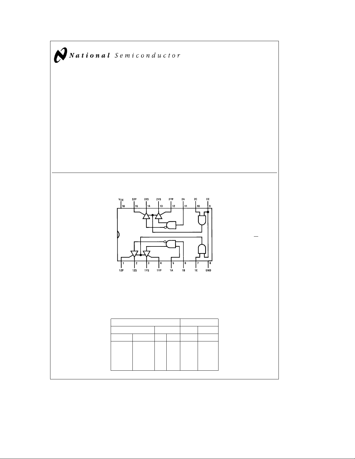
Connection Diagram
Dual-In-Line Package
Features
Y
Each circuit offers a choice of open-collector or active
pull-up (totem-pole) outputs
Y
Single 5V supply
Y
Differential line operation
Y
Dual channels
Y
TTL/LS compatibility
Y
High-impedance output state for party-line applications
Y
Short-circuit protection
Y
High current outputs
Y
Single-ended or differential AND/NAND outputs
Y
Common and individual output controls
Y
Clamp diodes at inputs
Y
Easily adaptable to DS55114/DS75114 applications
É
Positive logic: YeAB
Output is OFF when
CorCCislow
e
Z
AB
Order Number DS55113J, DS75113M or DS75113N
Top View
See NS Package Number J16A, M16A or N16A
For Complete Military 883 Specifications, see RETS Datasheet.
Order Number DS55113J/883
See NS Package Number J16A
Truth Table
Inputs Outputs
Output Control Data AND NAND
CCCAB*YZH
LXXXZZ
XLXXZZ
HHLXLH*
HHXLLH
HHHHHL
TRI-STATEÉis a registered trademark of National Semiconductor Corp.
C
1996 National Semiconductor Corporation RRD-B30M36/Printed in U. S. A.
TL/F/5785
TL/F/5785– 1
e
high level
Lelow level
e
X
irrelevant
e
high impedance (OFF)
Z
*B input and 4th line of truth
table applicable only to
driver number 1
http://www.national.com
Absolute Maximum Ratings (Note 1)
If Military/Aerospace specified devices are required,
please contact the National Semiconductor Sales
Office/Distributors for availability and specifications.
Supply Voltage (V
) (Note 1) 7V
CC
Input Voltage 5.5V
OFF-State Voltage Applied to
Open-Collector Outputs 12V
Maximum Power Dissipation* at 25
Cavity Package 1433 mW
C
§
Molded DIP Package 1362 mW
SO Package 1002 mW
Operating Free-Air Temperature Range
DS55113
DS75113 0
*Derate cavity package 9.6 mW/§C above 25§C; derate molded DIP pack-
age 10.9 mW/
(Note 2).
C above 25§C; derate SO package 8.01 mW/§C above 25§C
§
b
55§Ctoa125§C
Ctoa70§C
§
Storage Temperature Range
Lead Temperature (1/16×from case for
60 seconds): J Package 300
Lead Temperature (1/16
from case for
×
4 seconds): N Package 260
Operating Conditions
Supply Voltage (V
DS55113 4.5 5.5 V
DS75113 4.75 5.25 V
High Level Output Current (I
Low Level Output Current (IOL)40mA
Operating Free-Air Temperature (TA)
DS55113
DS75113 0 70
CC
)
)
OH
b
65§Ctoa150§C
Min Max Units
b
40 mA
b
55 125
Electrical Characteristics Over recommended operating free-air temperature range (unless otherwise noted)
Symbol Parameter Conditions (Note 3)
V
High Level
IH
Input Voltage
V
Low Level
IL
Input Voltage
e
V
Input Clamp Voltage V
IK
V
High Level V
OH
Output Voltage V
V
Low Level V
OL
Output Voltage
V
Output Clamp Voltage V
OK
I
Off-State V
O(off)
Open-Collector
CC
CC
IL
CC
CC
CC
e
Output Current
I
Off-State (High- V
OZ
Impedance-State) Output Controls
CC
Output Current at 0.8V
I
Input Current at A, B, C V
I
Maximum Input
Voltage
I
High Level A, B, C V
IH
Input Current
I
Low Level A, B, C V
IL
Input Current
CC
CC 2 2
CC
CC 80 80
CC
CC
Min, I
e
Min, V
0.8V
e
Min, V
e
Max, I
e
Max V
e
Max, T
e
Max, V
e
Max, V
e
Max, V
eb
12 mA
I
e
2V, I
IH
IH
O
I
I
I
e
eb
e
e
e
e
2V, V
0.8V, I
IL
40 mA
e
12V T
OH
e
V
5.25V T
OH
e
25§C, V
A
e
T
A
O
Max
5.5V 1 1
2.4V 40 40
0.4V
eb
10 mA 2.4 3.4 2.4 3.4
OH
eb
I
40 mA 2 3.0 2 3.0
OH
e
40 mA
OL
e
25§C110
A
e
T
125§C 200
A
e
25§C110
A
e
T
70§C20
A
e
0toV
CC
e
0V
V
O
e
0.4V
V
O
e
V
2.4V
O
e
V
V
O
CC
DS55113 DS75113
Typ
Min
(Note 4) (Note 4)
Max Min
Typ
22V
0.8 0.8 V
b
0.9b1.5
b
0.9b1.5 V
0.23 0.4 0.23 0.4 V
b
1.1b1.5
g
10
b
150
g
80
g
80
b
1.1b1.5 V
80 20
b
1.6
b
3.2
Max
g
10
b
20
g
20 mA
g
20
b
1.6
b
3.2
§
§
C
§
C
§
Units
mA
mA
mA
mA
C
C
V
http://www.national.com 2
Electrical Characteristics
Over recommended operating free-air temperature range (unless otherwise noted) (Continued)
Symbol Parameter Conditions (Note 3)
I
Short-Circuit Output V
OS
Current (Note 5)
I
Supply Current All Inputs at 0V, No Load V
CC
(Both Drivers) T
Note 1: All voltage values are with respect to network ground terminal.
Note 2: For operation above 25
Note 3: All parameters with the exception of OFF-state open-collector output current are measured with the active pull-up connected to the sink output.
Note 4: All typical values are at T
Note 5: Only one output should be shorted at a time, and duration of the short-circuit should not exceed one second.
C free-air temperature, refer to Dissipation Derating Curves in the Thermal information section.
§
e
A
CC
A
25§C and V
e
e
25§C
CC
e
Max, V
e
5V, with the exception of ICCat 7V.
0V
O
e
Max 47 65 47 65
CC
e
V
7V 65 85 65 85
CC
DS55113 DS75113
Typ
Min
(Note 4) (Note 4)
b40b90b
Max Min
120b40b90b120 mA
Typ
Units
Max
mA
Switching Characteristics V
CC
e
5V, C
L
e
30 pF, T
Symbol Parameter Conditions
t
t
t
t
t
t
PLH
PHL
PZH
PZL
PHZ
PLZ
Propagation Delay Time, Low-to
High-Level Output
Propagation Delay Time, High-to
Low-Level Output
Output Enable Time to High Level R
Output Enable Time to Low Level R
Output Disable Time from High R
Level
Output Disable Time from Low R
Level
(Figure 1)
e
180X,
L
e
250X,
L
e
180X,
L
e
250X,
L
(Figure 2)
(Figure 3)
(Figure 2)
(Figure 3)
e
25§C
A
DS55113 DS75113
Min Typ Max Min Typ Max
13 20 13 30 ns
12 20 12 30 ns
7 15 7 20 ns
14 30 14 40 ns
10 20 10 30 ns
17 35 17 35 ns
Unit
http://www.national.com3

Schematic Diagram (One side shown only)
Resistor values shown are typical and in X .
*These components common to both drivers.
TL/F/5785– 2
http://www.national.com 4

AC Test Circuits and Switching Time Waveforms
FIGURE 1. t
FIGURE 2. t
PLH
PZH
and t
and t
PHL
TL/F/5785– 3
TL/F/5785– 4
PHZ
Note 1: The pulse generator has the following characteristics: Z
Note 2: C
includes probe and jig capacitance.
L
FIGURE 3. t
e
50X, PRRe500 kHz, t
OUT
PZL
and t
PLZ
TL/F/5785– 5
e
100 ns.
W
http://www.national.com5

Typical Performance Characteristics
*
Output Voltage vs Output
Control Voltage
Output Voltage vs Free-Air
Temperature
Supply Current (Both
Drivers) vs Supply Voltage
Output Voltage vs Output
Control Voltage
High Level Output
Voltage vs Output
Current
Supply Current (Both
Drivers) vs Free-Air
Temperature
Output Voltage vs Output
Control Voltage
Low Level Output
Voltage vs Output
Current
Supply Current (Both
Drivers) vs Frequency
Propagation Delay Times
from Data Inputs vs Free-Air
Temperature
*Data for temperatures below 0§C and above 70§C and for supply voltages below 4.75V and above 5.25V are applicable to DS55113 circuits only. These
parameters were measured with the active pull-up connected to the sink output.
http://www.national.com 6
Output Enable and Disable
Times vs Free-Air Temperature
TL/F/5785– 7

Typical Performance Characteristics* (Continued)
Output Voltage vs Data
Input Voltage
*Data for temperatures below 0§C and above 70§C and for supply voltages below 4.75V and above 5.25V are applicable to DS55113 circuits only. These
parameters were measured with the active pull-up connected to the sink output.
Output Voltage vs Data
Input Voltage
Output Voltage vs Output
Control Voltage
TL/F/5785– 6
http://www.national.com7

Physical Dimensions inches (millimeters)
Ceramic Dual-In-Line Package (J)
Order Number DS55113J
NS Package Number J16A
http://www.national.com 8

Physical Dimensions inches (millimeters) (Continued)
SO Package (M)
Order Number DS75113M
NS Package Number M16A
http://www.national.com9

Physical Dimensions inches (millimeters) (Continued)
Molded Dual-In-Line Package (N)
Order Number DS75113N
NS Package Number N16A
DS55113/DS75113 Dual TRI-STATE Differential Line Driver
LIFE SUPPORT POLICY
NATIONAL’S PRODUCTS ARE NOT AUTHORIZED FOR USE AS CRITICAL COMPONENTS IN LIFE SUPPORT
DEVICES OR SYSTEMS WITHOUT THE EXPRESS WRITTEN APPROVAL OF THE PRESIDENT OF NATIONAL
SEMICONDUCTOR CORPORATION. As used herein:
1. Life support devices or systems are devices or 2. A critical component is any component of a life
systems which, (a) are intended for surgical implant support device or system whose failure to perform can
into the body, or (b) support or sustain life, and whose be reasonably expected to cause the failure of the life
failure to perform, when properly used in accordance support device or system, or to affect its safety or
with instructions for use provided in the labeling, can effectiveness.
be reasonably expected to result in a significant injury
to the user.
National Semiconductor National Semiconductor National Semiconductor National Semiconductor
Corporation Europe Hong Kong Ltd. Japan Ltd.
1111 West Bardin Road Fax:
Arlington, TX 76017 Email: europe.support@nsc.com Ocean Centre, 5 Canton Rd. Fax: 81-043-299-2408
Tel: 1(800) 272-9959 Deutsch Tel:
Fax: 1(800) 737-7018 English Tel:
http://www.national.com
National does not assume any responsibility for use of any circuitry described, no circuit patent licenses are implied and National reserves the right at any time without notice to change said circuitry and specifications.
Fran3ais Tel:
Italiano Tel:a49 (0) 180-534 16 80 Fax: (852) 2736-9960
a
49 (0) 180-530 85 86 13th Floor, Straight Block, Tel: 81-043-299-2308
a
49 (0) 180-530 85 85 Tsimshatsui, Kowloon
a
49 (0) 180-532 78 32 Hong Kong
a
49 (0) 180-532 93 58 Tel: (852) 2737-1600
 Loading...