

查询DP84240供应商
DP84240/DP84244 Octal TRI-STATEÉMOS Drivers
DP84240/DP84244 Octal TRI-STATE MOS Drivers
March 1986
General Description
The DP84240 and DP84244 are octal TRI-STATE drivers
which are designed for heavy capacitive load applications
such as fast data buffers or as memory address drivers. The
DP84240 is an inverting driver which is pin-compatible with
both the 74S240 and AM2965. The DP84244 is a non-inverting driver which is pin-compatible with the 74S244 and
AM2966. These parts are fabricated using an oxide isolation
process, for much faster speeds, and are specified for
250 pF and 500 pF load capacitances.
TRI-STATEÉis a registered trademark of National Semiconductor Corp.
Features
Y
tpdspecified with 250 pF and 500 pF loads
Y
Output specified from 0.8V to 2.7V
Y
Designed for symmetric rise and fall times at 500 pF
Y
Outputs glitch free at power up and power down
Y
PNP inputs reduce DC loading on bus lines
Y
Low static and dynamic input capacitance
Y
Low skew times between edges and pins
Y
AC parameters specified with all outputs switching
simultaneously
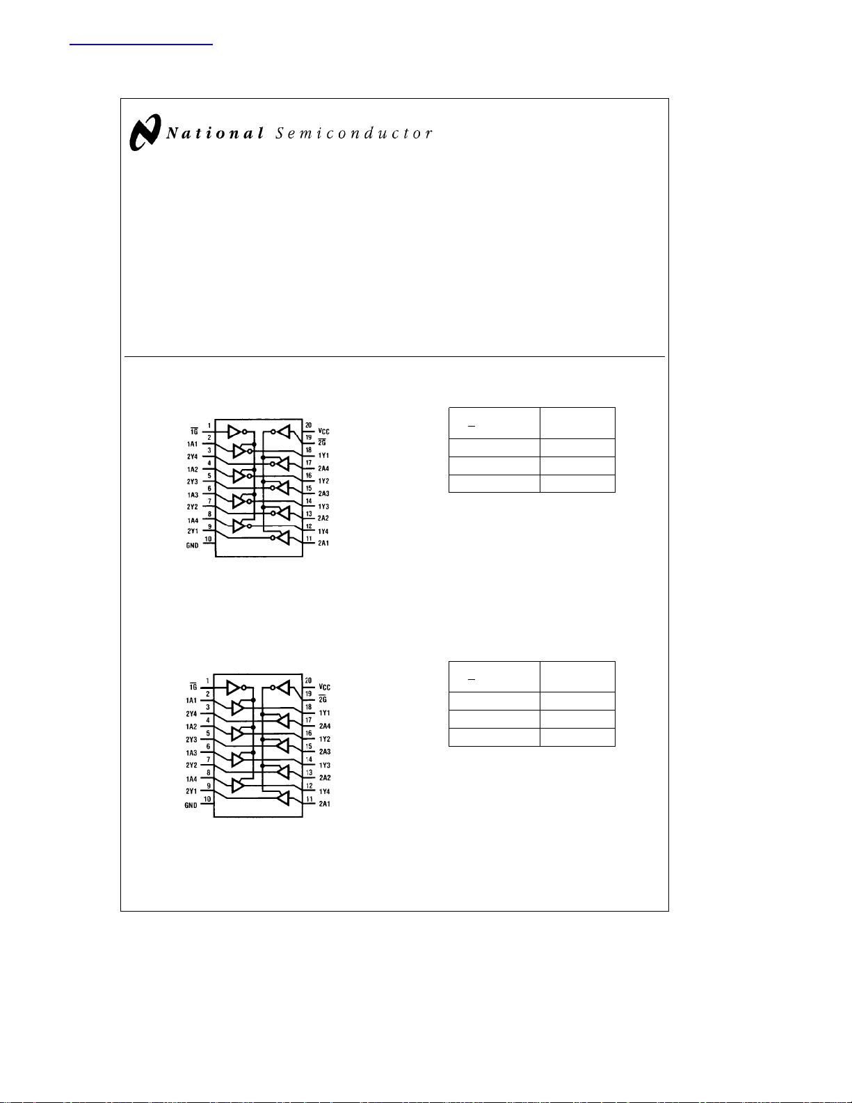
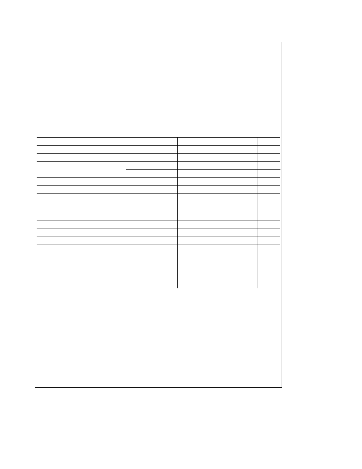
Connection Diagram Truth Table
DP84240
G
HX Z
LL H
LH L
e
H
High Level
e
L
Low Level
e
X
Don’t Care
e
Z
High Impedance
Top View
Order Number DP84240J or DP84240N
See NS Package Numbers J20A or N20A
TL/F/5219– 1
Inputs Outputs
AY
DP84244
Inputs Outputs
G
AY
HX Z
LL L
LH H
Top View
TL/F/5219– 2
Order Number DP84244J or DP84244N
See NS Package Numbers J20A or N20A
C
1995 National Semiconductor Corporation RRD-B30M105/Printed in U. S. A.
TL/F/5219
Absolute Maximum Ratings (Note 1)
If Military/Aerospace specified devices are required,
please contact the National Semiconductor Sales
Office/Distributors for availability and specifications.
Supply Voltage, V
CC
Logical ‘‘1’’ Input Voltage 7.0V
Logical ‘‘0’’ Input Voltage
Storage Temperature Range
b
65§Ctoa150§C
Power Dissipation
Cavity Package 1150 mW
Molded Package 1300 mW
Lead Temperature (soldering, 10 sec.) 300
7.0V
b
1.5V
Operating Conditions
V
Supply Voltage 4.5 5.5 V
CC
T
Ambient Temperature 0
A
C
§
Min Max Units
a
70
C
§
Electrical Characteristics V
e
5Vg10%, 0sT
CC
s
70§C. (Notes 2 and 3.)
A
Symbol Parameter Conditions Min Typ Max Units
V
IN(1)
V
IN(0)
I
IN(1)
I
IN(0)
V
CLAMP
V
OH
V
OL
I
1D
I
0D
Hi-Z TRI-STATE Output Current 0.4VsV
I
CC
Logical ‘‘1’’ Input Voltage 2.0 V
Logical ‘‘0’’ Input Voltage 0.8 V
Logical ‘‘1’’ Input Current V
Logical ‘‘0’’ Input Current 0sV
Input Clamp Voltage I
Logical ‘‘1’’ Output Voltage I
Logical ‘‘0’’ Output Voltage I
Logical ‘‘1’’ Drive Current V
Logical ‘‘0’’ Drive Current V
e
2.7V 0.1 20 mA
IN
e
V
7.0V 100 mA
IN
s
0.4V
IN
eb
18 mA
IN
eb
100 mAV
OH
eb
I
1mA V
OH
e
10 mA 0.2 0.4
OL
e
I
12 mA 0.3 0.5
OL
e
1.5V
OUT
e
1.5V
OUT
s
2.7V
OUT
–1.15 4.3
CC
b
1.5 3.9
CC
b
75
a
100
b
100
b
50
b
1
b
250 mA
a
150 mA
b
b
a
200 mA
1.2 V
100 mA
Supply Current All Outputs Open
DP84240 All Outputs High 16 50
V
V
All Outputs Low 74 125
All Outputs Hi-Z 80 125
DP84244 All Outputs High 40 75
mA
All Outputs Low 100 130
All Outputs Hi-Z 115 150
Note 1: ‘‘Absolute Maximum Ratings’’ are those values beyond which the safety of the device cannot be guaranteed. Except for ‘‘Operating Temperature Range’’
they are not meant to imply that the devices should be operated at these limits. The table of ‘‘Electrical Characteristics’’ provides conditions for actual device
operation.
Note 2: All currents into device pins shown as positive; all currents out of device pins shown as negative; all voltages referenced to ground unless otherwise noted.
All values shown as max. or min. are on an absolute value basis.
Note 3: Typical characteristics are taken at V
Note 4: The output-to-output skew is primarily a function of the number of outputs switching and the capacitive loading on those outputs. See
the switching time variations.
CC
e
5.0V and T
e
25§C.
A
Figures 5
and6for
2

Switching Characteristics V
tance and all eight outputs switching simultaneously. (Note 3.)
e
5Vg10%, 0sT
CC
s
70§C, all outputs loaded with specified load capaci-
A
Symbol Parameter Conditions Min Typ Max Units
t
PLH
t
PHL
t
PLZ
t
PHZ
t
PZL
t
PZH
t
SKEW
Propagation Delay from
Figures 1&3
LOW-to-HIGH Output C
Propagation Delay from C
HIGH-to-LOW Output C
Output Disable Time from LOW
Output Disable Time from HIGH
Output Enable Time to LOW
Output Enable Time to HIGH
Output-to-Output Skew (Note 4)
Figures 2&4,
Figures 2&4,
Figures 2&4,
Figures 2&4,
Figures 1&3,
Se1, C
L
Se2, C
L
Se1, C
L
Se2, C
L
e
C
500 pF 3 ns
L
CLe250 pF 9 16 27
e
500 pF 10 20 33
L
e
250 pF 9 16 25
L
e
500 pF 12 20 31
L
e
50 pF 11 24 ns
e
50 pF 12 24 ns
e
500 pF 30 45 ns
e
500 pF 23 35 ns
ns
ns
Capacitance T
e
25§C, fe1 MHz, V
A
e
5Vg10%. (Note 3.)
CC
Parameter Conditions Typ Units
C
IN
C
Note 1: ‘‘Absolute Maximum Ratings’’ are those values beyond which the safety of the device cannot be guaranteed. Except for ‘‘Operating Temperature Range’’
they are not meant to imply that the devices should be operated at these limits. The table of ‘‘Electrical Characteristics’’ provides conditions for actual device
operation.
Note 2: All currents into device pins shown as positive; all currents out of device pins shown as negative; all voltages referenced to ground unless otherwise noted.
All values shown as max. or min. are on an absolute value basis.
Note 3: Typical characteristics are taken at V
Note 4: The output-to-output skew is primarily a function of the number of outputs switching and the capacitive loading on those outputs. See
the switching time variations.
OUT
CC
e
All Other Inputs Tied Low 6 pF
Output in TRI-STATE Mode 20 pF
5.0V and T
e
25§C.
A
Figures 5
and6for
3

Switching Test Circuits
TL/F/5219– 3
*CLINCLUDES PROBE AND JIG CAPACITANCES
FIGURE 1. Capacitive Load Switching
Typical Switching Characteristics
Voltage Waveforms
TL/F/5219– 5
FIGURE 3. Output Drive Levels
TL/F/5219– 4
FIGURE 2. TRI-STATE Enable/Disable
TL/F/5219– 6
FIGURE 4. TRI-STATE Control Levels
FIGURE 5. t
Measured to 2.7V on Output vs. C
PLH
TL/F/5219– 7
L
4
FIGURE 6. t
Measured to 0.8V on Output vs. C
PHL
TL/F/5219– 8
L

Typical Switching Characteristics (Continued)
FIGURE 7. Typical Power Dissipation for DP84240 at
e
V
5.5V (All 8 drivers switching simultaneously)
CC
TL/F/5219– 9
Typical Application
DP84244 used as a buffer in a large memory array (greater than 88 dynamic RAMs)
FIGURE 8. Typical Power Dissipation for DP84244 at
e
V
5.5V (All 8 drivers switching simultaneously)
CC
TL/F/5219– 10
TL/F/5219– 11
5

Physical Dimensions inches (millimeters)
Order Number DP84240J/DP84244J
DP84240/DP84244 Octal TRI-STATE MOS Drivers
20-Lead Dual-In-Line Package (J)
NS Package Number J20A
20-Lead Dual-In-Line Package (N)
Order Number DP84240N/DP84244N
LIFE SUPPORT POLICY
NS Package Number N20A
NATIONAL’S PRODUCTS ARE NOT AUTHORIZED FOR USE AS CRITICAL COMPONENTS IN LIFE SUPPORT
DEVICES OR SYSTEMS WITHOUT THE EXPRESS WRITTEN APPROVAL OF THE PRESIDENT OF NATIONAL
SEMICONDUCTOR CORPORATION. As used herein:
1. Life support devices or systems are devices or 2. A critical component is any component of a life
systems which, (a) are intended for surgical implant support device or system whose failure to perform can
into the body, or (b) support or sustain life, and whose be reasonably expected to cause the failure of the life
failure to perform, when properly used in accordance support device or system, or to affect its safety or
with instructions for use provided in the labeling, can effectiveness.
be reasonably expected to result in a significant injury
to the user.
National Semiconductor National Semiconductor National Semiconductor National Semiconductor
Corporation Europe Hong Kong Ltd. Japan Ltd.
1111 West Bardin Road Fax: (
Arlington, TX 76017 Email: cnjwge@tevm2.nsc.com Ocean Centre, 5 Canton Rd. Fax: 81-043-299-2408
Tel: 1(800) 272-9959 Deutsch Tel: (
Fax: 1(800) 737-7018 English Tel: (
National does not assume any responsibility for use of any circuitry described, no circuit patent licenses are implied and National reserves the right at any time without notice to change said circuitry and specifications.
Fran3ais Tel: (
Italiano Tel: (
a
49) 0-180-530 85 86 13th Floor, Straight Block, Tel: 81-043-299-2309
a
49) 0-180-530 85 85 Tsimshatsui, Kowloon
a
49) 0-180-532 78 32 Hong Kong
a
49) 0-180-532 93 58 Tel: (852) 2737-1600
a
49) 0-180-534 16 80 Fax: (852) 2736-9960
 Loading...