

Page 1
查询DP83916供应商
DP83916 SONICTM-16
Systems-Oriented Network Interface Controller
General Description
The SONICTM-16 (Systems-Oriented Network Interface
Controller) is a second-generation Ethernet Controller designed to meet the demands of today’s high-speed 16-bit
systems. Its system interface operates with a high speed
DMA that typically consumes less than 8% of the bus bandwidth. Selectable bus modes provide both big and little endian byte ordering and a clean interface to standard microprocessors. The linked-list buffer management system of
SONIC-16 offers maximum flexibility in a variety of environments from PC-oriented adapters to high-speed motherboard designs. Furthermore, the SONIC-16 integrates a fully-compatible IEEE 802.3 Encoder/Decoder (ENDEC) allowing for a simple 2-chip solution for Ethernet when the
SONIC-16 is paired with the DP8392 Coaxial Transceiver
Interface.
For increased performance, the SONIC-16 implements a
unique buffer management scheme to efficiently process
receive and transmit packets in system memory. No intermediate packet copy is necessary. The receive buffer management uses three areas in memory for (1) allocating additional resources, (2) indicating status information, and (3)
buffering packet data. During reception, the SONIC-16
stores packets in the buffer area, then indicates receive
status and control information in the descriptor area. The
system allocates more memory resources to the SONIC-16
by adding descriptors to the memory resource area. The
transmit buffer management uses two areas in memory:
PRELIMINARY
November 1995
one for indicating status and control information and the
other for fetching packet data. The system can create a
transmit queue allowing multiple packets to be transmitted
from a single transmit command. The packet data can reside on any arbitrary byte boundary and can exist in several
non-contiguous locations.
Features
Y
23-bit non-multiplexed address/16-bit data bus
Y
High-speed, interruptible DMA
Y
Linked-list buffer management maximizes flexibility
Y
Two independent 32-byte transmit and receive FIFOs
Y
Bus compatibility for all standard microprocessors
Y
Supports big and little endian formats
Y
Integrated IEEE 802.3 ENDEC
Y
Complete address filtering for up to 16 physical and/or
multicast addresses
Y
32-bit general-purpose timer
Y
Full-duplex loopback diagnostics
Y
Fabricated in low-power CMOS
Y
132 PQFP package
Y
Full network management facilities support the IEEE
802.3 layer management standard
Y
Integrated support for bridge and repeater applications
DP83916 SONIC-16 Systems-Oriented Network Interface Controller
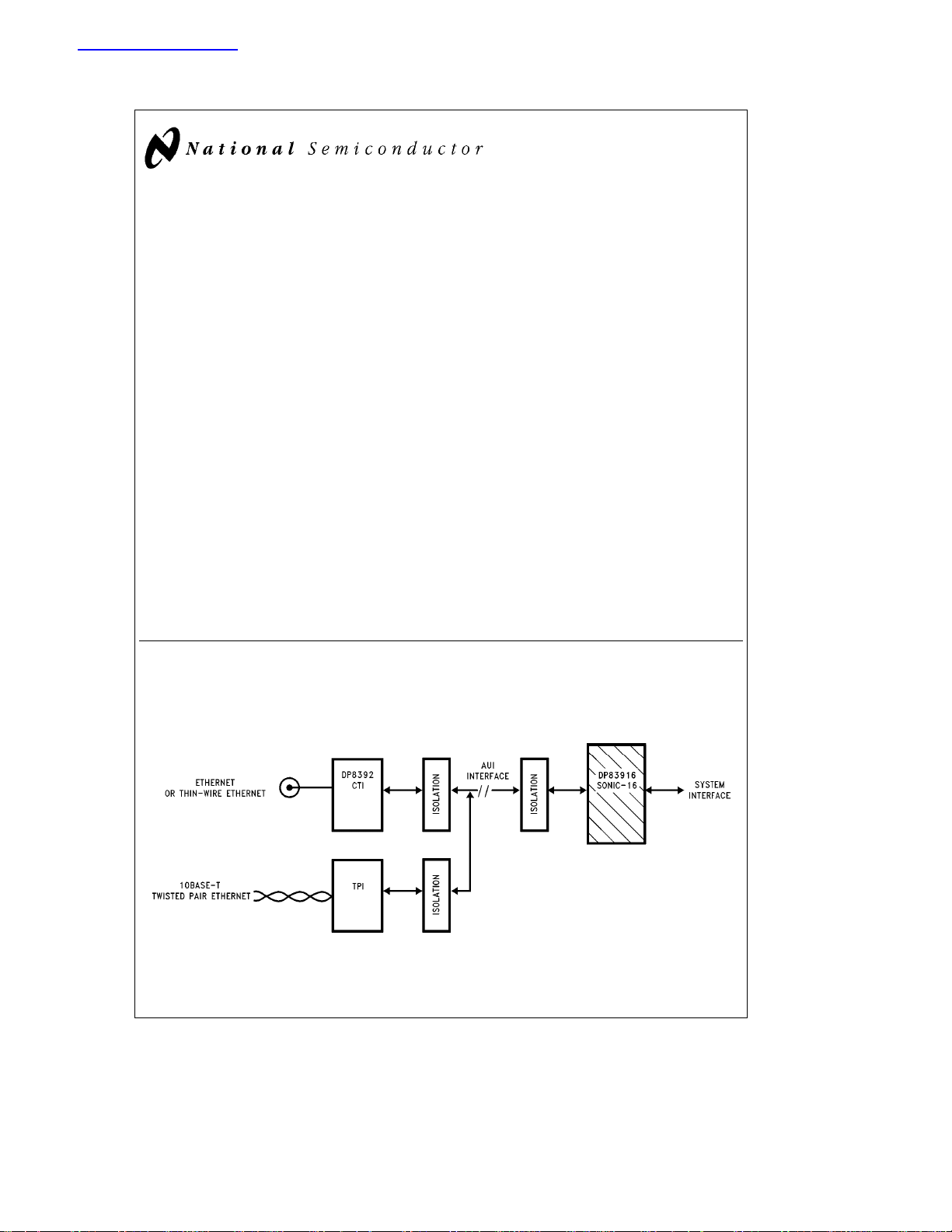
System Diagram
IEEE 802.3 Ethernet/Thin-Ethernet/10BASE-T Station
TL/F/11722– 1
TRI-STATEÉis a registered trademark of National Semiconductor Corporation.
TM
RIC
and SONICTM-16 are trademarks of National Semiconductor Corporation.
C
1995 National Semiconductor Corporation RRD-B30M16/Printed in U. S. A.
TL/F/11722
Page 2

1.0 FUNCTIONAL DESCRIPTION
1.1 IEEE 802.3 ENDEC Unit
1.1.1 ENDEC Operation
1.1.2 Selecting an External ENDEC
1.2 MAC Unit
1.2.1 MAC Receive Section
1.2.2 MAC Transmit Section
1.3 Byte Ordering
1.4 FIFO and Control Logic
1.4.1 Receive FIFO
1.4.2 Transmit FIFO
1.5 Status and Configuration Registers
1.6 Bus Interface
1.7 Loopback and Diagnostics
1.7.1 Loopback Procedure
1.8 Network Management Functions
2.0 TRANSMIT/RECEIVE IEEE 802.3
FRAME FORMAT
2.1 Preamble and Start Of Frame Delimiter (SFD)
2.2 Destination Address
2.3 Source Address
2.4 Length/Type Field
2.5 Data Field
2.6 FCS Field
2.7 MAC (Media Access Control) Conformance
3.0 BUFFER MANAGEMENT
3.1 Buffer Management Overview
3.2 Descriptor Areas
3.2.1 Naming Convention for Descriptors
3.2.2 Abbreviations
3.2.3 Buffer Management Base Address
3.3 Descriptor Data Alignment
3.4 Receive Buffer Management
3.4.1 Receive Resource Area (RRA)
3.4.2 Receive Buffer Area (RBA)
3.4.3 Receive Descriptor Area (RDA)
3.4.4 Receive Buffer Management Initialization
3.4.5 Beginning of Reception
3.4.6 End of Packet Processing
3.4.7 Overflow Conditions
3.5 Transmit Buffer Management
3.5.1 Transmit Descriptor Area (TDA)
3.5.2 Transmit Buffer Area (TBA)
3.5.3 Preparing to Transmit
3.5.4 Dynamically Adding TDA Descriptors
Table of Contents
4.0 SONIC-16 REGISTERS
4.1 The CAM Unit
4.1.1 The Load CAM Command
4.2 Status/Control Registers
4.3 Register Description
4.3.1 Command Register
4.3.2 Data Configuration Register
4.3.3 Receive Control Register
4.3.4 Transmit Control Register
4.3.5 Interrupt Mask Register
4.3.6 Interrupt Status Register
4.3.7 Data Configuration Register 2
4.3.8 Transmit Registers
4.3.9 Receive Registers
4.3.10 CAM Registers
4.3.11 Tally Counters
4.3.12 General Purpose Timer
4.3.13 Silicon Revision Register
5.0 BUS INTERFACE
5.1 Pin Configurations
5.2 Pin Description
5.3 System Configuration
5.4 Bus Operations
5.4.1 Acquiring the Bus
5.4.2 Block Transfers
5.4.3 Bus Status
5.4.4 Bus Mode Compatibility
5.4.5 Master Mode Bus Cycles
5.4.6 Bus Exceptions (Bus Retry)
5.4.7 Slave Mode Bus Cycle
5.4.8 On-Chip Memory Arbiter
5.4.9 Chip Reset
6.0 NETWORK INTERFACING
6.1 Manchester Encoder and Differential Driver
6.1.1 Manchester Decoder
6.1.2 Collision Translator
6.1.3 Oscillator Inputs
7.0 AC AND DC SPECIFICATIONS
8.0 AC TIMING TEST CONDITIONS
2
Page 3
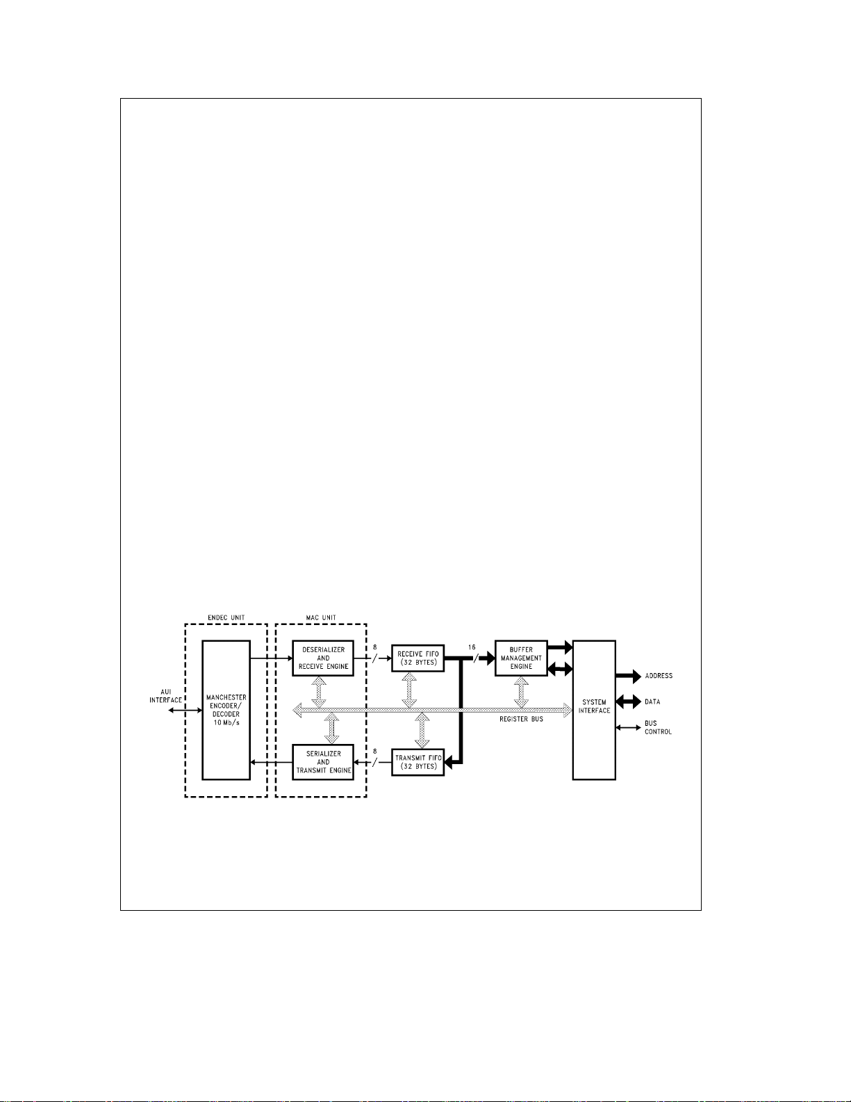
1.0 Functional Description
The SONIC-16
(ENDEC) unit, media access control (MAC) unit, separate
receive and transmit FIFOs, a system buffer management
engine, and a user programmable system bus interface unit
on a single chip. SONIC-16 is highly pipelined providing
maximum system level performance. This section provides
a functional overview of SONIC-16.
1.1 IEEE 802.3 ENDEC UNIT
The ENDEC (Encoder/Decoder) unit is the interface between the Ethernet transceiver and the MAC unit. It provides the Manchester data encoding and decoding functions for IEEE 802.3 Ethernet/Thin-Ethernet type local area
networks. The ENDEC operations of SONIC-16 are identical
to the DP83910A CMOS Serial Network Interface device.
During transmission, the ENDEC unit combines non-returnzero (NRZ) data from the MAC section and clock pulses into
Manchester data and sends the converted data differentially
to the transceiver. Conversely, during reception, an analog
PLL decodes the Manchester data to NRZ format and receive clock. The ENDEC unit is a functionally complete
Manchester encoder/decoder incorporating a balanced
driver and receiver, on-board crystal oscillator, collision signal translator, and a diagnostic loopback. The features include:
Compatible with Ethernet I and II, IEEE 802.3 10BASE5
#
and 10BASE2
10Mb/s Manchester encoding/decoding with receive
#
clock recovery
Requires no precision components
#
Loopback capability for diagnostics
#
Externally selectable half or full step modes of operation
#
at transmit output
Squelch circuitry at the receive and collision inputs reject
#
noise
Connects to the transceiver (AUI) cable via external
#
pulse transformer
(Figure 1-1 )
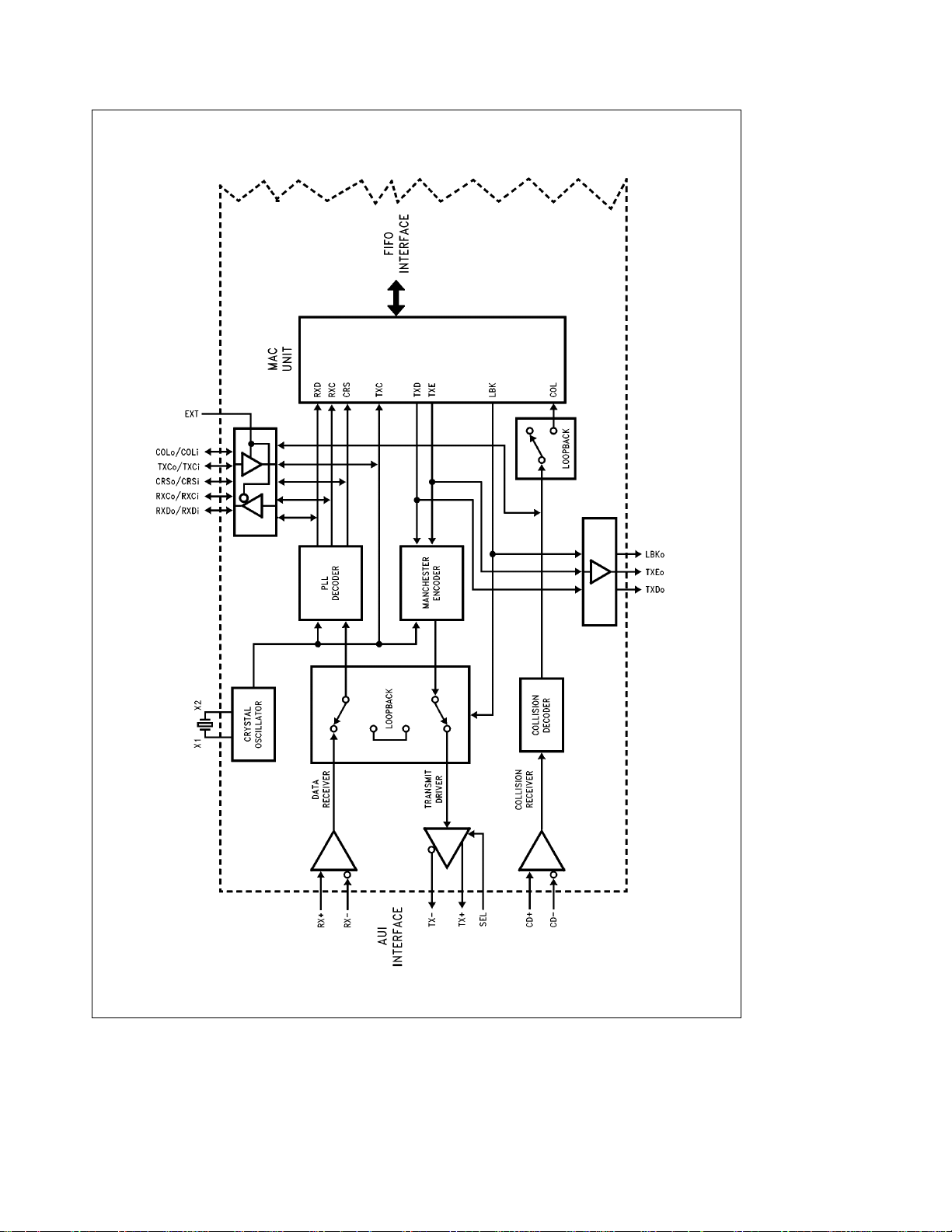
consists of an encoder/decoder
1.1.1 ENDEC Operation
The primary function of the ENDEC unit
perform the encoding and decoding necessary for compatibility between the differential pair Manchester encoded data
of the transceiver and the Non-Return-to-Zero (NRZ) serial
data of the MAC unit data line. In addition to encoding and
decoding the data stream, the ENDEC also supplies all the
necessary special signals (e.g., collision detect, carrier
sense, and clocks) to the MAC unit.
Manchester Encoder and Differential Output Driver:
During transmission to the network, the ENDEC unit translates the NRZ serial data from the MAC unit into differential
pair Manchester encoded data on the Coaxial Transceiver
Interface (e.g., National’s DP8392) transmit pair. To perform
this operation the NRZ bit stream from the MAC unit is
passed through the Manchester encoder block of the ENDEC unit. Once the bit stream is encoded, it is transmitted
out differentially to the transmit differential pair through the
transmit driver.
Manchester Decoder: During reception from the network,
the differential receive data from the transceiver (e.g., the
DP8392) is converted from Manchester encoded data into
NRZ serial data and a receive clock, which are sent to the
receive data and clock inputs of the MAC unit. To perform
this operation the signal, once received by the differential
receiver, is passed to the phase locked loop (PLL) decoder
block. The PLL decodes the data and generates a data receive clock and a NRZ serial data stream to the MAC unit.
Special Signals: In addition to performing the Manchester
encoding and decoding function, the ENDEC unit provides
control and clocking signals to the MAC unit. The ENDEC
sends a carrier sense (CRS) signal that indicates to the
MAC unit that data is present from the network on the ENDEC’s receive differential pair. The MAC unit is also provided with a collision detection signal (COL) that informs the
MAC unit that a collision is taking place somewhere on the
(Figure 1-2 )
is to
FIGURE 1-1. SONIC-16 Block Diagram
3
TL/F/11722– 2
Page 4
1.0 Functional Description (Continued)
TL/F/11722– 3
FIGURE 1-2. Block Diagram of Ethernet ENDEC
4
Page 5
1.0 Functional Description (Continued)
network. The ENDEC section detects this when its collision
receiver detects a 10 MHz signal on the differential collision
input pair. The ENDEC also provides both the receive and
transmit clocks to the MAC unit. The transmit clock is one
half of the oscillator input. The receive clock is extracted
from the input data by the PLL.
Oscillator: The oscillator generates the 10 MHz transmit
clock signal for network timing. The oscillator is controlled
by a parallel resonant crystal or by an external clock (see
section 6.1.3). The 20 MHz output of the oscillator is divided
by 2 to generate the 10 MHz transmit clock (TXC) for the
MAC section. The oscillator provides an internal clock signal
for the encoding and decoding circuits.
The signals provided to the MAC unit from the on-chip ENDEC are also provided as outputs to the user.
Loopback Functions: The SONIC-16 provides three loopback modes. These modes allow loopback testing at the
MAC, ENDEC and external transceiver level (see section
1.7 for details). It is important to note that when the SONIC16 is transmitting, the transmitted packet will always be
looped back by the external transceiver. The SONIC-16
takes advantage of this to monitor the transmitted packet.
See the explanation of the Receive State Machine in section 1.2.1 for more information about monitoring transmitted
packets.
1.1.2 Selecting An External ENDEC
An option is provided on SONIC-16 to disable the on-chip
ENDEC unit and use an external ENDEC. The internal IEEE
802.3 ENDEC can be bypassed by connecting the EXT pin
to V
(EXTe1). In this mode the MAC signals are redirect-
CC
ed out from the chip, allowing an external ENDEC to be
used. See section 5.2 for the alternate pin definitions.
1.2 MAC UNIT
The MAC (Media Access Control) unit performs the media
access control functions for transmitting and receiving packets over Ethernet. During transmission, the MAC unit frames
information from the transmit FIFO and supplies serialized
data to the ENDEC unit. During reception, the incoming information from the ENDEC unit is deserialized, the frame
checked for valid reception, and the data is transferred to
the receive FIFO. Control and status registers on the
SONIC-16 govern the operation of the MAC unit.
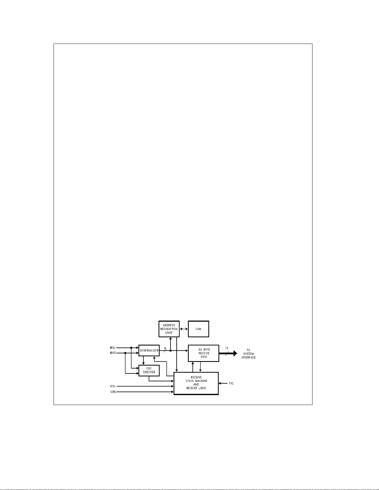
1.2.1 MAC Receive Section
The receive section
operations during reception, loopback, and transmission.
During reception, the deserializer goes active after detecting
the 2-bit SFD (Start of Frame Delimiter) pattern (section
2.1). It then frames the incoming bits into octet boundaries
(Figure 1-3 )
controls the MAC receive
and transfers the data to the 32-byte receive FIFO. Concurrently the address comparator compares the Destination
Address Field to the addresses stored in the chip’s CAM
address registers (Content Addressable Memory cells). If a
match occurs, the deserializer passes the remainder of the
packet to the receive FIFO. The packet is decapsulated
when the carrier sense input pin (CRS) goes inactive. At the
end of reception the receive section checks the following:
Ð Frame alignment errors
Ð CRC errors
Ð Length errors (runt packets)
The appropriate status is indicated in the Receive Control
register (section 4.3.3). In loopback operations, the receive
section operates the same as during normal reception.
During transmission, the receive section remains active to
allow monitoring of the self-received packet. The CRC
checker operates as normal, and the Source Address field
is compared with the CAM address entries. Status of the
CRC check and the source address comparison is indicated
by the PMB bit in the Transmit Control register (section
4.3.4). No data is written to the receive FIFO during transmit
operations.
The receive section consists of the following blocks detailed
below.
Receive State Machine (RSM): The RSM insures the proper sequencing for normal reception and self-reception during transmission. When the network is inactive, the RSM
remains in an idle state continually monitoring for network
activity. If the network becomes active, the RSM allows the
deserializer to write data into the receive FIFO. During this
state, the following conditions may prevent the complete
reception of the packet.
Ð FIFO OverrunÐThe receive FIFO has been completely
filled before the SONIC-16 could buffer the data to memory.
Ð CAM Address MismatchÐThe packet is rejected be-
cause of a mismatch between the destination address of
the packet and the address in the CAM.
Ð Memory Resource ErrorÐThere are no more resources
(buffers) available for buffering the incoming packets.
Ð Collision or Other ErrorÐA collision occured on the net-
work or some other error, such as a CRC error, occurred
(this is true if the SONIC-16 has been told to reject packets on a collision, or reject packets with errors).
If these conditions do not occur, the RSM processes the
packet indicating the appropriate status in the Receive Control register.
FIGURE 1-3. MAC Receiver
5
TL/F/11722– 4
Page 6
1.0 Functional Description (Continued)
During transmission of a packet from the SONIC-16, the
external transceiver will always loop the packet back to the
SONIC-16. The SONIC-16 will use this to monitor the packet
as it is being transmitted. The CRC and source address of
the looped back packet are checked with the CRC and
source address that were transmitted. If they do not match,
an error bit is set in the status of the transmitted packet (see
Packet Monitored Bad, PBM, in the Transmit Control Register, section 4.3.4). Data is not written to the receive FIFO
during this monitoring process unless Transceiver Loopback
mode has been selected (see section 1.7).
Receive Logic: The receive logic contains the command,
control, and status registers that govern the operations of
the receive section. It generates the control signals for writing data to the receive FIFO, processes error signals obtained from the CRC checker and the deserializer, activates
the ‘‘packet reject’’ signal to the RSM for rejecting packets,
and posts the applicable status in the Receive Control register.
Deserializer: This section deserializes the serial input data
stream and furnishes a byte clock for the address comparator and receive logic. It also synchronizes the CRC checker
to begin operation (after SFD is detected), and checks for
proper frame alignment with respect to CRS going inactive
at the end of reception.
Address Comparator: The address comparator latches the
Destination Address (during reception or loopback) or
Source Address (during transmission) and determines
whether the address matches one of the entries in the CAM
(Content Addressable Memory).
CRC Checker: The CRC checker calculates the 4-byte
Frame Check Sequence (FCS) field from the incoming data
stream and compares it with the last 4-bytes of the received
packet. The CRC checker is active for both normal reception and self-reception during transmission.
Content Addressable Memory (CAM): The CAM contains
16 user programmable entries and 1 pre-programmed
Broadcast address entry for complete filtering of received
packets. The CAM can be loaded with any combination of
Physical and Multicast Addresses (section 2.2). See section
4.1 for the procedure on loading the CAM registers.
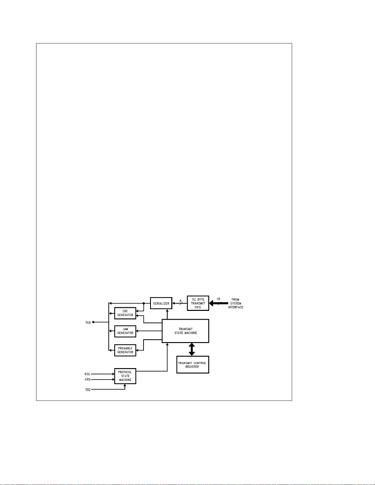
1.2.2 MAC Transmit Section
The transmit section
data from the transmit FIFO and transmitting a serial data
(Figure 1-4 )
is responsible for reading
stream onto the network in conformance with the IEEE
802.3 CSMA/CD standard. The Transmit Section consists
of the following blocks.
Transmit State Machine (TSM): The TSM controls the
functions of the serializer, preamble generator, and JAM
generator. It determines the proper sequence of events that
the transmitter follows under various network conditions. If
no collision occurs, the transmitter prefixes a 62-bit preamble and 2-bit Start of Frame Delimiter (SFD) at the beginning
of each packet, then sends the serialized data. At the end of
the packet, an optional 4-byte CRC pattern is appended. If a
collision occurs, the transmitter switches from transmitting
data to sending a 4-byte Jam pattern to notify all nodes that
a collision has occurred. Should the collision occur during
the preamble, the transmitter waits for it to complete before
jamming. After the transmission has completed, the transmitter writes status in the Transmit Control register (section
4.3.4).
Protocol State Machine: The protocol state machine assures that the SONIC-16 obeys the CSMA/CD protocol. Before transmitting, this state machine monitors the carrier
sense and collision signals for network activity. If another
node(s) is currently transmitting, the SONIC-16 defers until
the network is quiet, then transmits after its Interframe Gap
Timer (9.6 ms) has expired. The Interframe Gap time is divided into two portions. During the first 6.4 ms, network activity
restarts the Interframe Gap timer. Beyond this time, however, network activity is ignored and the state machine waits
the remaining 3.2 ms before transmitting. If the SONIC-16
experiences a collision during a transmission, the SONIC-16
switches from transmitting data to a 4-byte JAM pattern (4
bytes of all 1’s), before ceasing to transmit. The SONIC-16
then waits a random number of slot times (51.2 ms) determined by the
rithm
rithm, the number of slot times to delay before the nth retransmission is chosen to be a random integer r in the range
of:
If a collision occurs on the 16th transmit attempt, the SONIC-16 aborts transmitting the packet and reports an ‘‘Excessive Collisions’’ error in the Transmit Control register.
Truncated Binary Exponential Backoff Algo-
before reattempting another transmission. In this algo-
k
srs
0
2
where kemin(n,10)
FIGURE 1-4. MAC Transmitter
6
TL/F/11722– 5
Page 7
1.0 Functional Description (Continued)
Serializer: After data has been written into the 32-byte
transmit FIFO, the serializer reads byte wide data from the
FIFO and sends a NRZ data stream to the Manchester encoder. The rate at which data is transmitted is determined
by the transmit clock (TXC). The serialized data is transmitted after the SFD.
Preamble Generator: The preamble generator prefixes a
62-bit alternating ‘‘1,0’’ pattern and a 2-bit ‘‘1,1’’ SFD pattern at the beginning of each packet. This allows receiving
nodes to synchronize to the incoming data. The preamble is
always transmitted in its entirety even in the event of a collision. This assures that the minimum collision fragment is 96
bits (64 bits of normal preamble, and 4 bytes, or rather 32
bits, of the JAM pattern).
CRC Generator: The CRC generator calculates the 4-byte
FCS field from the transmitted serial data stream. If enabled, the 4-byte FCS field is appended to the end of the
transmitted packet (section 2.6).
Jam Generator: The Jam generator produces a 4-byte pattern of all 1’s to assure that all nodes on the network sense
the collision. When a collision occurs, the SONIC-16 stops
transmitting data and enables the Jam generator. If a collision occurs during the preamble, the SONIC-16 finishes
transmitting the preamble before enabling the Jam generator (see Preamble Generator above).
1.3 BYTE ORDERING
The SONIC-16 will operate with 16-bit wide memory. The
SONIC-16 provides both Little Endian and Big Endian byte-
ordering capability for compatibility with National/Intel or
Motorola microprocessors respectively by selecting the
proper level on the BMODE pin. The byte ordering is depicted as follows:
Little Endian mode (BMODE
received and transmitted data in the Receive Buffer Area
(RBA) and Transmit Buffer Area (TBA) of system memory is
as follows:
15 8 7 0
Byte 1 Byte 0
MSB LSB
Big Endian mode (BMODE
received and transmitted data in the RBA and TBA is as
follows:
15 8 7 0
Byte 0 Byte 1
LSB MSB
e
0): The byte orientation for
16-Bit Word
e
1): The byte orientation for
16-Bit Word
FIGURE 1-5. Receive FIFO
7
TL/F/11722– 6
Page 8

1.0 Functional Description (Continued)
1.4 FIFO AND CONTROL LOGIC
The SONIC-16 incorporates two independent 32-byte
FIFOs for transferring data to/from the system interface and
from/to the network. The FIFOs, providing temporary storage of data, free the host system from the real-time demands on the network.
The way in which the FIFOS are emptied and filled is controlled by the FIFO threshold values and the Block Mode
Select bits (BMS, section 4.3.2). The threshold values determine how full or empty the FIFOs can be before the SONIC16 will request the bus to get more data from memory or
buffer more data to memory. When block mode is set, the
number of bytes transferred is set by the threshold value.
For example, if the threshold for the receive FIFO is 4
words, then the SONIC-16 will always transfer 4 words from
the receive FIFO to memory. If empty/fill mode is set, however, the number of bytes transferred is the number required
to fill the transmit FIFO or empty the receive FIFO. More
specific information about how the threshold affects reception and transmission of packets is discussed in sections
1.4.1 and 1.4.2 below.
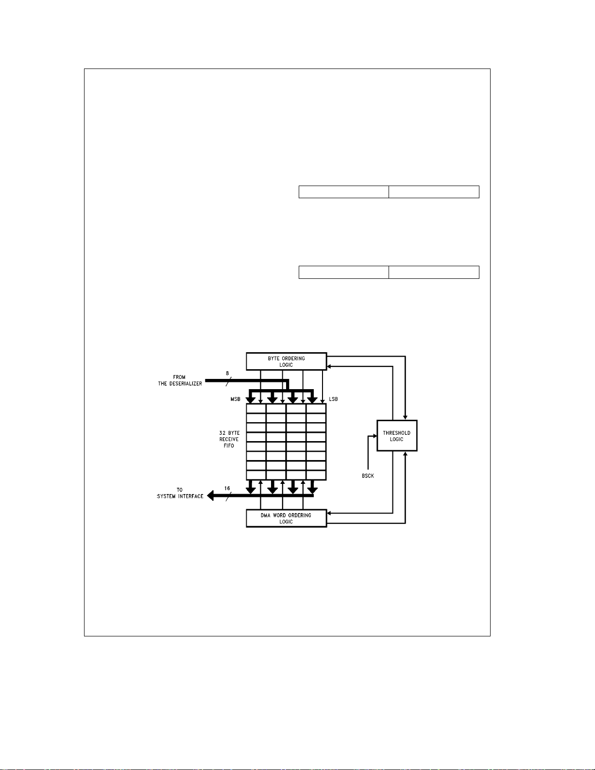
1.4.1 Receive FIFO
To accommodate the different transfer rates, the receive
FIFO
(Figure 1-5 )
work (deserializer) interface and the 16-bit system interface.
The FIFO is arranged as a 4-byte wide by 8 deep memory
array (8 long words, or 32 bytes) controlled by three sections of logic. During reception, the Byte Ordering logic directs the byte stream from the deserializer into the FIFO
using one of four write pointers. Depending on the selected
byte-ordering mode, data is written either least significant
byte first or most significant byte first to accommodate little
or big endian byte-ordering formats respectively.
As data enters the FIFO, the Threshold Logic monitors the
number of bytes written in from the deserializer. The programmable threshold (RFT1,0 in the Data Configuration
Register) determines the number of words (or long words)
written into the FIFO from the MAC unit before a DMA request for system memory occurs. When the threshold is
reached, the Threshold Logic enables the Buffer Management Engine to read a programmed number of 16-bit words
(depending upon the selected word width) from the FIFO
and transfers them to the system interface (the system
memory) using DMA. The threshold is reached when the
number of bytes in the receive FIFO is greater than the
value of the threshold. For example, if the threshold is 4
words (8 bytes), then the Threshold Logic will not cause the
Buffer Management Engine to write to memory until there
are more than 8 bytes in the FIFO.
The Buffer Management Engine reads either the upper or
lower half (16 bits) of the FIFO. If, after the transfer is complete, the number of bytes in the FIFO is less then the
threshold, then the SONIC-16 is done. This is always the
case when the SONIC-16 is in empty/fill mode. If, however,
for some reason (e.g. latency on the bus) the number of
bytes in the FIFO is still greater than the threshold value,
the Threshold Logic will cause the Buffer Management Engine to do a DMA request to write to memory again. This
later case is usually only possible when the SONIC-16 is in
block mode.
When in block mode, each time the SONIC-16 requests the
bus, only a number of bytes equal to the threshold value will
serves as a buffer between the 8-bit net-
be transferred. The Threshold Logic continues to monitor
the number of bytes written in from the deserializer and enables the Buffer Management Engine every time the threshold has been reached. This process continues until the end
of the packet.
Once the end of the packet has been reached, the serializer
will fill out the last word if the last byte did not end on a word
boundary. The fill byte will be 0FFh. Immediately after the
last byte (or fill byte) in the FIFO, the received packets
status will be written into the FIFO. The entire packet, including any fill bytes and the received packet status will be
buffered to memory. When a packet is buffered to memory
by the Buffer Management Engine, it is always taken from
the FIFO in words and buffered to memory on word boundaries. Data from a packet cannot be buffered on odd byte
boundaries (see Section 3.3). For more information on the
receive packet buffering process, see Section 3.4.
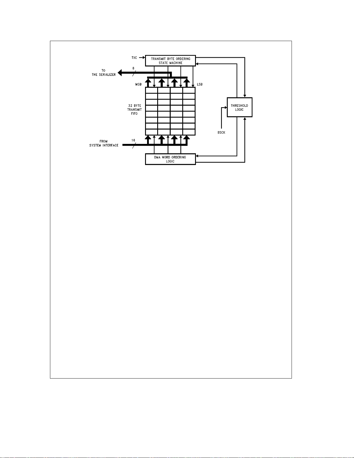
1.4.2 Transmit FIFO
Similar to the Receive FIFO, the Transmit FIFO
serves as a buffer between the 16-bit system interface and
the network (serializer) interface. The Transmit FIFO is also
arranged as a 4 byte by 8 deep memory array (8 long words
or 32 bytes) controlled by three sections of logic. Before
transmission can begin, the Buffer Management Engine
fetches a programmed number of 16-bit words from memory and transfers them to the FIFO. The Buffer Management
Engine writes either the upper or lower half (16 bits) into the
FIFO.
The Threshold logic monitors the number of bytes as they
are written into the FIFO. When the threshold has been
reached, the Transmit Byte Ordering state machine begins
reading bytes from the FIFO to produce a continuous byte
stream for the serializer. The threshold is met when the
number of bytes in the FIFO is greater than the value of the
threshold. For example, if the transmit threshold is 4 words
(8 bytes), the Transmit Byte Ordering state machine will not
begin reading bytes from the FIFO until there are 9 or more
bytes in the buffer. The Buffer Management Engine continues replenishing the FIFO until the end of the packet. It
does this by making multiple DMA requests to the system
interface. Whenever the number of bytes in the FIFO is
equal to or less than the threshold value, the Buffer Management Engine will do a DMA request. If block mode is set,
then after each request has been granted by the system,
the Buffer Management Engine will transfer a number of
bytes equal to the threshold value into the FIFO. If empty/fill
mode is set, the FIFO will be completely filled in one DMA
request.
Since data may be organized in big or little endian byte ordering format, the Transmit Byte Ordering state machine
uses one of four read pointers to locate the proper byte
within the 4 byte wide FIFO. It also determines the valid
number of bytes in the FIFO. For packets which begin or
end at odd bytes in the FIFO, the Buffer Management Engine writes extraneous bytes into the FIFO. The Transmit
Byte Ordering state machine detects these bytes and only
transfers the valid bytes to the serializer. The Buffer Management Engine can read data from memory on any byte
boundary (see Section 3.3). See Section 3.5 for more information on transmit buffering.
(Figure 1-6 )
8
Page 9
1.0 Functional Description (Continued)
FIGURE 1-6. Transmit FIFO
1.5 STATUS AND CONFIGURATION REGISTERS
The SONIC-16 contains a set of status/control registers for
conveying status and control information to/from the host
system. The SONIC-16 uses these registers for loading
commands generated from the system, indicating transmit
and receive status, buffering data to/from memory, and providing interrupt control. Each register is 16 bits in length.
See section 4.0 for a description of the registers.
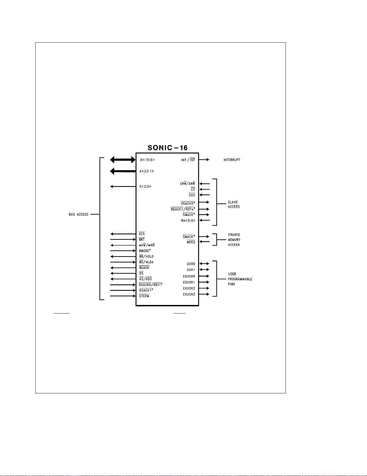
1.6 BUS INTERFACE
The system interface
essary for interfacing to a variety of buses. It includes the
I/O drivers for the data and address lines, bus access control for standard microprocessors, ready logic for synchronous or asynchronous systems, slave access control, interrupt control, and shared-memory access control. The functional signal groups are shown in
for a complete description of the SONIC-16 bus interface.
1.7 LOOPBACK AND DIAGNOSTICS
The SONIC-16 furnishes three loopback modes for selftesting from the controller interface to the transceiver interface. The loopback function is provided to allow self-testing
of the chip’s internal transmit and receive operations. During
loopback, transmitted packets are routed back to the receive section of the SONIC-16 where they are filtered by the
address recognition logic and buffered to memory if accepted. Transmit and receive status and interrupts remain active
during loopback. This means that when using loopback, it is
as if the packet was transmitted and received by two separate chips that are connected to the same bus and memory.
MAC Loopback: Transmitted data is looped back at the
MAC. Data is not sent from the MAC to either the internal
ENDEC or an external ENDEC (the external ENDEC interface pins will not be driven), hence, data is not transmitted
from the chip. Even though the ENDEC is not used in MAC
loopback, the ENDEC clock (an oscillator or crystal for the
internal ENDEC or TXC for an external ENDEC) must be
driven. Network activity, such as a collision, does not affect
(Figure 1-7 )
consists of the pins nec-
Figure 1-7
. See section 5.0
TL/F/11722– 7
MAC loopback. CSMA/CD MAC protocol is not completely
followed in MAC loopback.
ENDEC Loopback: Transmitted data is looped back at the
ENDEC. If the internal ENDEC is used, data is switched
from the transmit section of the ENDEC to the receive section (
Figure 1-2
the collision lines, CD
ty does not affect ENDEC loopback. The LBK signal from
the MAC tells the internal ENDEC to go into loopback mode.
If an external ENDEC is used, it should operate in loopback
mode when the LBK signal is asserted. CSMA/CD MAC
protocol is followed even though data is not transmitted
from the chip.
Transceiver Loopback: Transmitted data is looped back at
the external transceiver (which is always the case regardless of the SONIC-16’s loopback mode). CSMA/CD MAC
protocol is followed since data will be transmitted from the
chip. This means that transceiver loopback is affected by
network activity. The basic difference between Transceiver
Loopback and normal, non-loopback, operations of the
SONIC-16 is that in Transceiver Loopback, the SONIC-16
loads the receive FIFO and buffers the packet to memory. In
normal operations, the SONIC-16 only monitors the packet
that is looped back by the transceiver, but does not fill the
receive FIFO and buffer the packet.
1.7.1 Loopback Procedure
The following procedure describes the loopback operation.
1. Initialize the Transmit and Receive Area as described in
Sections 3.4 and 3.5.
2. Load one of the CAM address registers (see Section 4.1),
with the Destination Address of the packet if you are verifying the SONIC-16’s address recognition capability.
3. Load one of the CAM address registers with the Source
Address of the packet if it is different than the Destination
Address to avoid getting a Packet Monitored Bad (PMB)
error in the Transmit status (see Section 4.3.4).
). Data is not transmitted from the chip and
g
, are ignored, hence, network activi-
9
Page 10
1.0 Functional Description (Continued)
4. Program the Receive Control register with the desired receive filter and the loopback mode (LB1, LB0).
5. Issue the transmit command (TXP) and enable the receiver (RXEN) in the Command register.
The SONIC-16 completes the loopback operation after the
packet has been completely received (or rejected if there is
an address mismatch). The Transmit Control and Receive
Control registers treat the loopback packet as in normal operation and indicate status accordingly. Interrupts are also
generated if enabled in the Interrupt Mask register.
Note: For MAC Loopback, only one packet may be queued for proper oper-
ation. This restriction occurs because the transmit MAC section,
which does not generate an Interframe Gap time (IFG) between
transmitted packets, does not allow the receive MAC section to update receive status. There are no restrictions for the other loopback
modes.
1.8 NETWORK MANAGEMENT FUNCTIONS
The SONIC-16 fully supports the Layer Management IEEE
802.3 standard to allow a node to monitor the overall performance of the network. These statistics are available on a
per packet basis at the end of reception or transmission. In
addition, the SONIC-16 provides three tally counters to tabulate CRC errors, Frame Alignment errors, and missed
packets. Table 1-1 shows the statistics indicated by the
SONIC-16.
*Note: DSACK0,1 are used for both Bus and Slave Access Control and are bidirectional. SMACK is used for both Slave access and shared memory access. The
BMODE pin selects between National/Intel or Motorola type buses.
TL/F/11722– 8
FIGURE 1-7. SONIC-16 Interface Signals
10
Page 11
1.0 Functional Description (Continued)
TABLE 1-1. Network Management Statistics
Statistic Register Used Bits Used
Frames Transmitted OK TCR (Note) PTX
Single Collision Frames (Note) NC0–NC4
Multiple Collision Frames (Note) NC0–NC4
Collision Frames (Note) NC0–NC4
Frames with Deferred Transmissions TCR (Note) DEF
Late Collisions TCR (Note) OWC
Excessive Collisions TCR (Note) EXC
Excessive Deferral TCR (Note) EXD
Internal MAC Transmit Error TCR (Note) BCM, FU
Frames Received OK RCR (Note) PRX
Multicast Frames Received OK RCR (Note) MC
Broadcast Frames Received OK RCR (Note) BC
Frame Check Sequence Errors CRCT All
Alignment Errors FAET All
Frame Lost due to Internal MAC Receive Error MPT All
Note: The number of collisions and the contents of the Transmit Control register are posted in the TXpkt.status field (see
section 3.5.1.2). The contents of the Receive Control register are posted in the RXpkt.status field (see section 3.4.3.1).
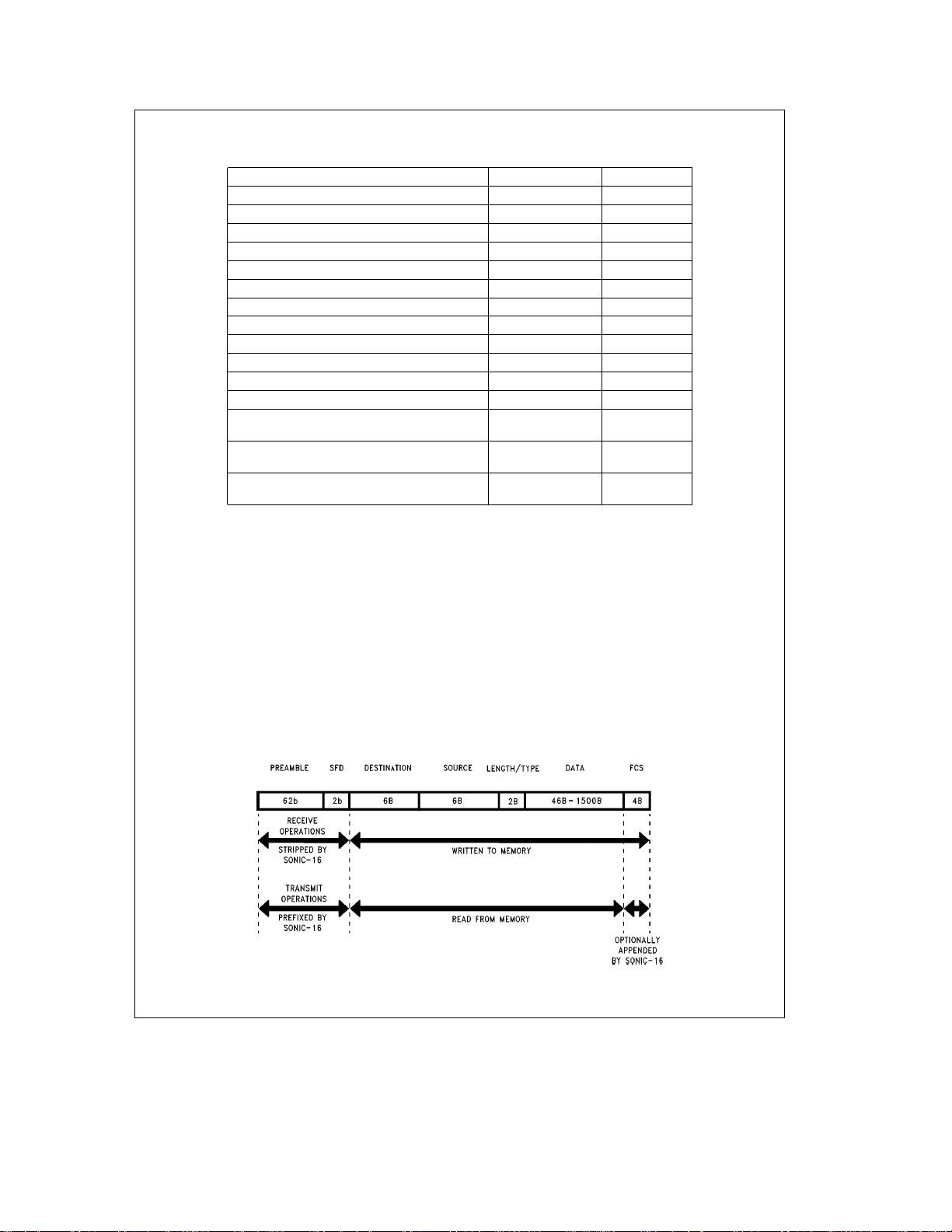
2.0 Transmit/Receive IEEE 802.3 Frame Format
A standard IEEE 802.3 packet
following fields: preamble, Start of Frame Delimiter (SFD),
destination address, source address, length, data and
Frame Check Sequence (FCS). The typical format is shown
in
Figure 2-1
decoded by the ENDEC unit and transferred serially to/from
the MAC unit using NRZ data with a clock. All fields are of
fixed length except for the data field. The SONIC-16 generates and appends the preamble, SFD and FCS field during
transmission. The Preamble and SFD fields are stripped
during reception. (The CRC is passed through to buffer
memory during reception.)
. The packets are Manchester encoded and
(Figure 2-1 )
consists of the
2.1 PREAMBLE AND START OF FRAME DELIMITER
(SFD)
The Manchester encoded alternating 1,0 preamble field is
used by the ENDEC to acquire bit synchronization with an
incoming packet. When transmitted, each packet contains
62 bits of an alternating 1,0 preamble. Some of this preamble may be lost as the packet travels through the network.
Byte alignment is performed when the Start of Frame Delimiter (SFD) pattern, consisting of two consecutive 1’s, is detected.
2.2 DESTINATION ADDRESS
The destination address indicates the destination of the
packet on the network and is used to filter unwanted pack-
RCR CRC
RCR FAE
ISR RFO
Note: Bebytes
bebits TL/F/11722– 9
FIGURE 2-1. IEEE 802.3 Packet Structure
11
Page 12
2.0 Transmit/Receive IEEE 802.3 Frame Format (Continued)
ets from reaching a node. There are three types of address
formats supported by the SONIC-16: Physical, Multicast,
and Broadcast.
Physical Address: The physical address is a unique address that corresponds only to a single node. All physical
addresses have the LSB of the first byte of the address set
to ‘‘0’’. These addresses are compared to the internally
stored CAM (Content Addressable Memory) address entries. All bits in the destination address must match an entry
in the CAM in order for the SONIC-16 to accept the packet.
Multicast Address: Multicast addresses, which have the
LSB of the first byte of the address set to ‘‘1’’, are treated
similarly as Physical addresses, i.e., they must match an
entry in the CAM. This allows perfect filtering of Multicast
packet’s and eliminates the need for a hashing algorithm for
mapping Multicast packets.
Broadcast Address: If the address consists of all 1’s, it is a
Broadcast address, indicating that the packet is intended for
all nodes.
The SONIC-16 also provides a promiscuous mode which
allows reception of all physical address packets. Physical,
Multicast, Broadcast, and promiscuous address modes can
be selected via the Receive Control register.
2.3 SOURCE ADDRESS
The source address is the physical address of the sending
node. Source addresses cannot be multicast or broadcast
addresses. This field must be passed to the SONIC-16’s
transmit buffer from the system software. During transmission, the SONIC-16 compares the Source address with its
internal CAM address entries before monitoring the CRC of
the self-received packet. If the source address of the packet
transmitted does not match a value in the CAM, the packet
monitored bad flag (PMB) will be set in the transmit status
field of the transmit descriptor (see Sections 3.5.1.2 and
4.3.4). The SONIC-16 does not provide Source Address in-
sertion. However, a transmit descriptor fragment, containing
only the Source Address, may be created for each packet.
(See Section 3.5.1.)
2.4 LENGTH/TYPE FIELD
For IEEE 802.3 type packets, this field indicates the number
of bytes that are contained in the data field of the packet.
For Ethernet I and II networks, this field indicates the type of
packet. The SONIC-16 does not operate on this field.
2.5 DATA FIELD
The data field has a variable octet length ranging from 46 to
1500 bytes as defined by the Ethernet specification. Messages longer than 1500 bytes need to be broken into multiple packets for IEEE 802.3 networks. Data fields shorter
than 46 bytes require appending a pad to bring the complete frame length to 64 bytes. If the data field is padded,
the number of valid bytes are indicated in the length field.
The SONIC-16 does not append pad bytes for short packets
during transmission, nor check for oversize packets during
reception. However, the user’s driver software can easily
append the pad by lengthening the TXpkt.pktÐsize field
and TXpkt.fragÐsize field(s) to at least 64 bytes (see Section 3.5.1). While the Ethernet specification defines the
maximum number of bytes in the data field the SONIC-16
can transmit and receive packets up to 64k bytes.
2.6 FCS FIELD
The Frame Check Sequence (FCS) is a 32-bit CRC field
calculated and appended to a packet during transmission to
allow detection of error-free packets. During reception, an
error-free packet results in a specific pattern in the CRC
generator. The AUTODIN II (X32
X16aX12aX11aX10aX8aX7aX5aX4
X2aX1a1) polynomial is used for the CRC calculations.
The SONIC-16 may optionally append the CRC sequence
during transmission, and checks the CRC both during normal reception and self-reception during a transmission (see
Section 1.2.1).
2.7 MAC (MEDIA ACCESS CONTROL) CONFORMANCE
The SONIC-16 is designed to be compliant to the IEEE
802.3 MAC Conformance specification. The SONIC-16 implements most of the MAC functions in silicon and provides
hooks for the user software to handle the remaining functions. The MAC Conformance specifications are summarized in Table 2-1.
TABLE 2-1. MAC Conformance Specifications
Conformance
Test Name
Minimum Frame Size X
Maximum Frame Size X X 1
Address Generation X X 2
Address Recognition X
Pad Length Generation X X 3
Start Of Frame Delimiter X
Length Field X
Preamble Generation X
Order of Bit Transmission X
Inconsistent Frame Length X X 1
Non-Integral Octet Count X
Incorrect Frame Check
Sequence
Frame Assembly X
FCS Generation and Insertion X
Carrier Deference X
Interframe Spacing X
Collision Detection X
Collision Handling X
Collision Backoff and
Retransmission
FCS Validation X
Frame Disassembly X
Back-to-Back Frames X
Flow Control X
Attempt Limit X
Jam Size (after SFD) X
Jam Size (in Preamble) X
Note 1: The SONIC-16 provides the byte count of the entire packet in the
RXpkt.byteÐcount (see Section 3.4.3). The user’s driver software may perform further filtering of the packet based upon the byte count.
Note 2: The SONIC-16 does not provide Source Address insertion; however,
a transmit descriptor fragment, containing only the Source Address, may be
created for each packet. See Section 3.5.1.
Note 3: The SONIC-16 does not provide Pad generation; however, the user’s driver software can easily append the Pad by lengthening the
TXpkt.pktÐsize field and TXpkt.fragÐsize field(s) to at least 64 bytes. See
Section 3.5.1.
12
a
X26aX23aX22
Support By
SONIC User Driver
-16 Software
X
X
a
a
Notes
Page 13

3.0 Buffer Management
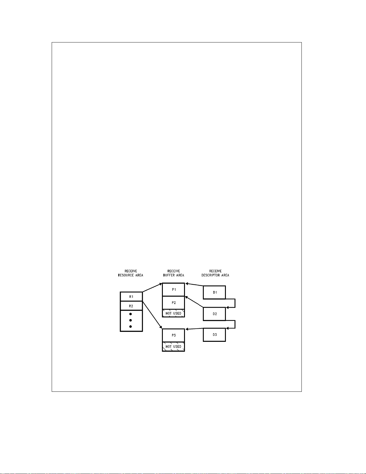
3.1 BUFFER MANAGEMENT OVERVIEW
The SONIC-16’s buffer management scheme is based on
separate buffers and descriptors (
Packets that are received or transmitted are placed in buffers called the Receive Buffer Area (RBA) and the Transmit
Buffer Area (TBA). The system keeps track of packets in
these buffers using the information in the Receive Descriptor Area (RDA) and the Transmit Descriptor Area (TDA). A
single (TDA) points to a single TBA, but multiple RDAs can
point to a single RBA (one RDA per packet in the buffer).
The Receive Resource Area (RRA), which is another form
of descriptor, is used to keep track of the actual buffer.
When packets are transmitted, the system sets up the packets in one or more TBAs with a TDA pointing to each TBA.
There can only be one packet per TBA/TDA pair. A single
packet, however, may be made up of several fragments of
data dispersed in memory. There is one TDA pointing to
each packet which specifies information about the packet’s
size, location in memory, number of fragments and status
after transmission. The TDAs are linked together in a linked
list. The system causes the SONIC-16 to transmit the packets by passing the first TDA to the SONIC-16 and issuing
the transmit command.
Before a packet can be received, an RBA and RDA must be
set up by the system. RDAs are made up as a linked list
similar to TDAs. An RDA is not linked to a particular RBA,
though. Instead, an RDA is linked specifically to a packet
after it has been buffered into an RBA. More than one packet can be buffered into the same RBA, but each packet gets
its own RDA. A received packet can not be scattered into
fragments. The system only needs to tell the SONIC-16
where the first RDA and where the RBAs are. Since an RDA
never specifically points to an RBA, the RRA is used to
keep track of the RBAs. The RRA is a circular queue of
pointers and buffer sizes (not a linked list). When the SONIC-16 receives a packet, it is buffered into a RBA and a RDA
is written to so that it points to and describes the new packet. If the RBA does not have enough space to buffer the
next packet, a new RBA is obtained from the RRA.
3.2 DESCRIPTOR AREAS
Descriptors are the basis of the buffer management scheme
used by the SONIC-16. A RDA points to a received packet
within a RBA, a RRA points to a RBA and a TDA points to a
TBA which contains a packet to be transmitted. The conventions and registers used to describe these descriptors
are discussed in the next three sections.
3.2.1 Naming Convention for Descriptors
The fields which make up the descriptors are named in a
consistent manner to assist in remembering the usage of
each descriptor. Each descriptor name consists of three
components in the following format.
[
RX/TX][descriptor name].[field
The first two capital letters indicate whether the descriptor is
used for transmission (TX) or reception (RX), and is then
followed by the descriptor name having one of two names.
Figures 3-2
and
3-11
]
e
rsrc
Resource descriptor
e
pkt
Packet descriptor
).
The last component consists of a field name to distinguish it
from the other fields of a descriptor. The field name is separated from the descriptor name by a period (‘‘.’’). An example of a descriptor is shown below.
RX rsrc buffÐptr 0,1
Descriptor consists of two
fields. ‘‘0’’ and ‘‘1’’
respectively indicate the
least and most significant
portions of the descriptor.
The ‘‘pointer’’ field of the
descriptor
A descriptor for a buffer
resource
A descriptor used for
reception
3.2.2 Abbreviations
The abbreviations in Table 3-1 are used to describe the
SONIC-16 registers and data structures in memory. The ‘‘0’’
and ‘‘1’’ in the abbreviations indicate the least and most
significant portions of the registers or descriptors. Table 3-1
lists the naming convention abbreviations for descriptors.
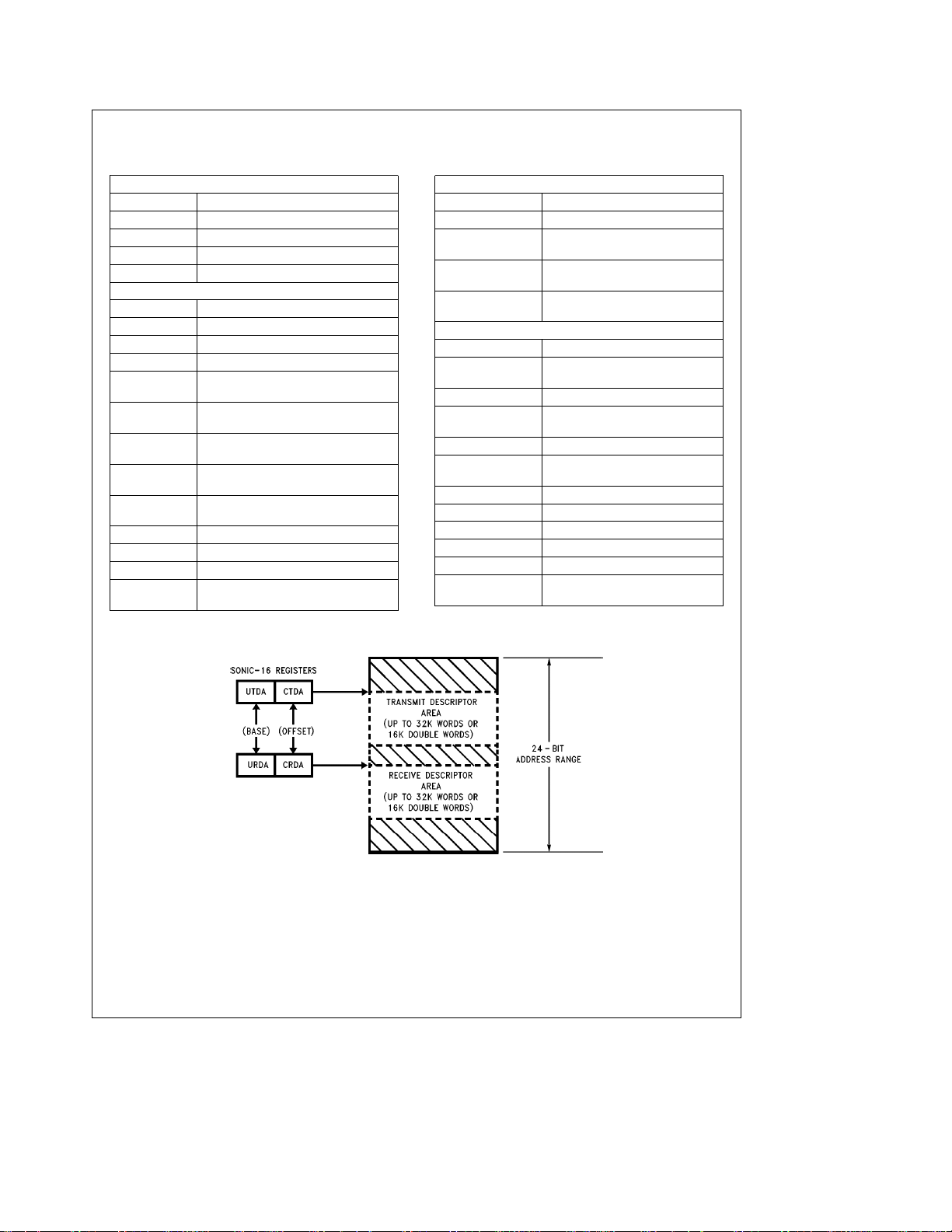
3.2.3 Buffer Management Base Addresses
The SONIC-16 uses three areas in memory to store descriptor information: the Transmit Descriptor Area (TDA), Receive Descriptor Area (RDA), and the Receive Resource
Area (RRA). The SONIC-16 accesses these areas by concatenating a 16-bit base address register with a 16-bit offset
register. The base address register supplies a fixed upper 8
bits of address and the offset registers provide the lower 16
bits of address. The base address registers are the Upper
Transmit Descriptor Address (UTDA), Upper Receive Descriptor Address (URDA), and the Upper Receive Resource
Address (URRA) registers. The corresponding offset registers are shown below.
Upper Address Registers Offset Registers
See Table 3-1 for definition of register mnemonics.
Figure 3-1
Area and the Receive Descriptor Area being located by the
UTDA and URDA registers. The descriptor areas, RDA,
TDA, and RRA are allowed to have the same base address.
i.e., URRA
to prevent these areas from overwriting each other.
URRA RSA,REA,RWP,RRP
URDA CRDA
UTDA CTDA
shows an example of the Transmit Descriptor
e
URDAeUTDA. Care, however, must be taken
13
Page 14
3.0 Buffer Management (Continued)
TABLE 3-1. Descriptor Abbreviations
TRANSMIT AND RECEIVE AREAS
RRA Receive Resource Area
RDA Receive Descriptor Area
RBA Receive Buffer Area
TDA Transmit Descriptor Area
TBA Transmit Buffer Area
BUFFER MANAGEMENT REGISTERS
RSA Resource Start Area Register
REA Resource End Area Register
RRP Resource Read Pointer Register
RWP Resource Write Pointer Register
CRDA Current Receive Descriptor
Address Register
CRBA0,1 Current Receive Buffer Address
Register
TCBA0,1 Temporary Current Buffer Address
Register
RBWC0,1 Remaining Buffer Word Count
Register
TRBWC0,1 Temporary Remaining Buffer Word
Count Register
EOBC End of Buffer Count Register
TPS Transmit Packet Size Register
TSA0,1 Transmit Start Address Register
CTDA Current Transmit Descriptor
Address Register
BUFFER MANAGEMENT REGISTERS (Continued)
TFC Transmit Fragment Count Register
TFS Transmit Fragment Size Register
UTDA Upper Transmit Descriptor
Address Register
URRA Upper Receive Resource Address
Register
URDA Upper Receive Descriptor Address
Register
TRANSMIT AND RECEIVE DESCRIPTORS
RXrsrc.buffÐptr0,1 Buffer Pointer Field in the RRA
RXrsrc.buffÐwc0,1 Buffer Word Count Fields in the
RRA
RXpkt.status Receive Status Field in the RDA
RXpkt.byteÐcount Packet Byte Count Field in the
RDA
RXpkt.buffÐptr0,1 Buffer Pointer Fields in the RDA
RXpkt.link Receive Descriptor Link Field in
RDA
RXpkt.inÐuse ‘‘In Use’’ Field in RDA
TXpkt.fragÐcount Fragment Count Field in TDA
TXpkt.pktÐsize Packet Size Field in TDA
TXpkt.pktÐptr0,1 Packet Pointer Fields in TDA
TXpkt.fragÐsize Fragment Size Field in TDA
TXpkt.link Transmit Descriptor Link Field in
TDA
FIGURE 3-1. Transmit and Receive Descriptor Area Pointers
14
TL/F/11722– 10
Page 15
3.0 Buffer Management (Continued)
3.3 DESCRIPTOR DATA ALIGNMENT
All fields used by descriptors (RXpkt.xxx, RXrsrc.xxx, and
TXpkt.xxx) are word quantities (16-bit) and must be aligned
to word boundaries (A0
(RBA) must also be aligned to a word boundary. The fragments in the Transmit Buffer Area (TBA), however, may be
aligned on any arbitrary byte boundary.
All descriptor areas follow little endian byte ordering, even
when BMODE
3.4 RECEIVE BUFFER MANAGEMENT
The Receive Buffer Management operates on three areas in
memory into which data, status, and control information are
written during reception
must be initialized (section 3.4.4) before enabling the receiver (setting the RXEN bit in the Command register). The receive resource area (RRA) contains descriptors that locate
receive buffer areas in system memory. These descriptors
are denoted by R1, R2, etc. in
by P1, P2, etc.) can then be buffered into the corresponding
RBAs. Depending on the size of each buffer area and the
size of the packet(s), multiple or single packets are buffered
into each RBA. The receive descriptor area (RDA) contains
status and control information for each packet (D1, D2, etc.
in
Figure 3-2
goes with P1, D2 with P2, etc.).
When a packet arrives, the address recognition logic checks
the address for a Physical, Multicast, or Broadcast match
and if the packet is accepted, the SONIC-16 buffers the
packet contiguously into the selected Receive Buffer Area
(RBA). Because of the previous end-of-packet processing,
the SONIC-16 assures that the complete packet is written
into a single contiguous block. When the packet ends, the
SONIC-16 writes the receive status, byte count, and location of the packet into the Receive Descriptor Area (RDA).
The SONIC-16 then updates its pointers to locate the next
available descriptor and checks the remaining words available in the RBA. If sufficient space remains, the SONIC-16
buffers the next packet immediately after the previous pack-
e
) corresponding to each received packet (D1
1.
e
0). The Receive Buffer Area
(Figure 3-2 )
. These three areas
Figure 3-2
. Packets (denoted
et. If the current buffer is out of space the SONIC-16 fetches
a Resource descriptor from the Receive Resource Area
(RRA) acquiring an additional buffer that has been previously allocated by the system.
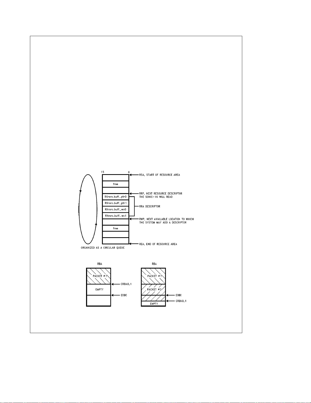
3.4.1 Receive Resource Area (RRA)
As buffer memory is consumed by the SONIC-16 for storing
data, the Receive Resource Area (RRA) provides a mechanism that allows the system to allocate additional buffer
space for the SONIC-16. The system loads this area with
resource descriptors that the SONIC-16, in turn, reads as its
current buffer space is used up. Each resource descriptor
consists of a 23-bit buffer pointer locating the starting point
of the RBA and a 32-bit Word Count that indicates the size
of the buffer in words (2 bytes per word). The buffer pointer
and word count are contiguously located using the format
shown in
Figure 3-3
bit fields. The SONIC-16 stores this information internally
and concatenates the corresponding fields to create 23and 32-bit long words for the buffer pointer and word count.
The SONIC-16 organizes the RRA as a circular queue for
efficient processing of descriptors. Four registers define the
RRA. The first two, the Resource Start Area (RSA) and the
Resource End Area (REA) registers, determine the starting
and ending locations of the RRA, and the other two registers update the RRA. The system adds descriptors at the
address specified by the Resource Write Pointer (RWP),
and the SONIC-16 reads the next descriptor designated by
the Resource Read Pointer (RRP). The RRP is advanced 4
words after the SONIC-16 finishes reading the RRA and
automatically wraps around to the beginning of the RRA
once the end has been reached. When a descriptor in the
RRA is read, the RXrsc.buffÐpt0,1 is loaded into the
CRBA0,1 registers and the RXrsc.buffÐwc0,1 is loaded into
the RBWC0,1 registers.
The alignment of the RRA is confined to word boundaries
(A0 is always zero).
with each component composed of 16-
FIGURE 3-2. Overview of Receive Buffer Management
15
TL/F/11722– 11
Page 16
3.0 Buffer Management (Continued)
3.4.2 Receive Buffer Area (RBA)
The SONIC-16 stores the actual data of a received packet
in the RBA. The RBAs are designated by the resource descriptors in the RRA as described above. The
RXrsrc.buffÐwc0,1 fields of the RRA indicate the length of
the RBA. When the SONIC-16 gets a RBA from the RRA,
the RXrsrc.buffÐwc0,1 values are loaded into the Remaining Buffer Word Count registers (RBWC0,1). These registers keep track of how much space (in words) is left in the
buffer. When a packet is buffered in a RBA, it is buffered
contiguously (the SONIC-16 will not scatter a packet into
multiple buffers or fragments). Therefore, if there is not
enough space left in a RBA after buffering a packet to buffer
at least one more maximum sized packet (the maximum
legal sized packet expected to be received from the network), a new buffer must be acquired. The End of Buffer
Count (EOBC) register is used to tell the SONIC-16 the maximum packet size that the SONIC-16 will need to buffer.
3.4.2.1 End of Buffer Count (EOBC)
The EOBC is a boundary in the RBA based from the bottom
of the buffer. The value written into the EOBC is the maximum expected size (in words) of the network packet that
the SONIC-16 will have to buffer. This word count creates a
line in the RBA that, when crossed, causes the SONIC-16 to
fetch a new RBA resource from the RRA.
Note: The EOBC is a word count, not a byte count.
3.4.2.2 Buffering the Last Packet in an RBA
At the start of reception, the SONIC-16 stores the packet
beginning at the Current Receive Buffer Address (CRBA0,1)
and continues until the reception is complete. Concurrent
with reception, the SONIC-16 decrements the Remaining
Buffer Word Count (RBWC0,1) by one. At the end of reception, if the packet has crossed the EOBC boundary, the
SONIC-16 knows that the next packet might not fit in the
RBA. This check is done by comparing the RBWC0,1 registers with the EOBC. If RBWC0,1 is less than the EOBC (the
last packet buffered has crossed the EOBC boundary), the
SONIC-16 fetches the next resource descriptor in the RRA.
If RBWC0,1 is greater than or equal to the EOBC (the EOBC
boundary has not been crossed) the next packet reception
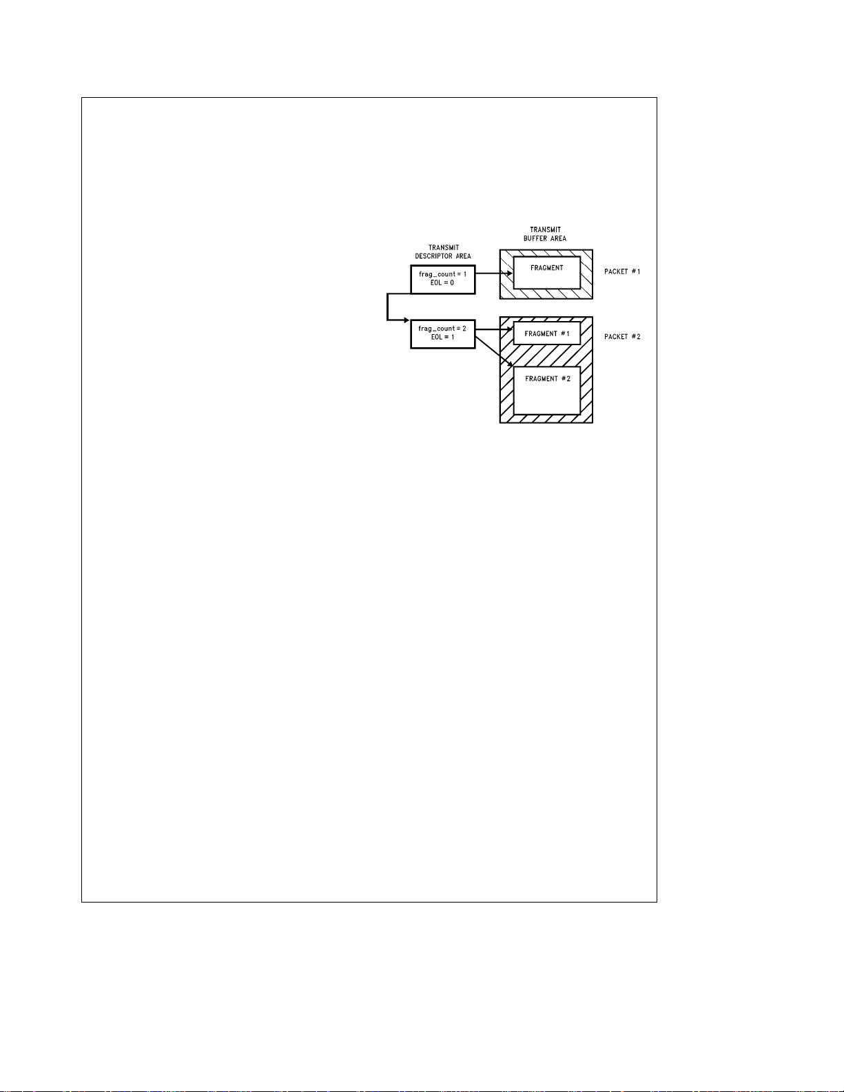
continues at the present location pointed to by CRBA0,1 in
the same RBA.
tions for (1) RBWC0,1
Figure 3-4
illustrates the SONIC-16’s ac-
t
EOBC and (2) RBWC0,1kEOBC.
See Section 3.4.4.4 for specific information about setting
the EOBC.
Note: It is important that the EOBC boundary be ‘‘crossed.’’ In other words,
Ý
1in
Figure 3-4
case
occurs without case
k
EOBC will not work properly and the SONIC-16 will not fetch a new
buffer. The result of this will be a buffer overflow (RBAE in the Interrupt Status Register, section 4.3.6).
must exist before caseÝ2 exists. If caseÝ2
Ý
1 having occurred first, the test for RBWC0,1
FIGURE 3-3. Receive Resource Area Format
CaseÝ1
t
Case
Case
(RBWC0,1
Ý
Ý
EOBC)
1: SONIC-16 buffers next packet in same RBA.
2: SONIC-16 detects an exhausted RBA and will buffer the next packet in another RBA.
Ý
Case
(RBWC0,1
2
k
EOBC)
FIGURE 3-4. Receive Buffer Area
16
TL/F/11722– 12
TL/F/11722– 13
Page 17
3.0 Buffer Management (Continued)
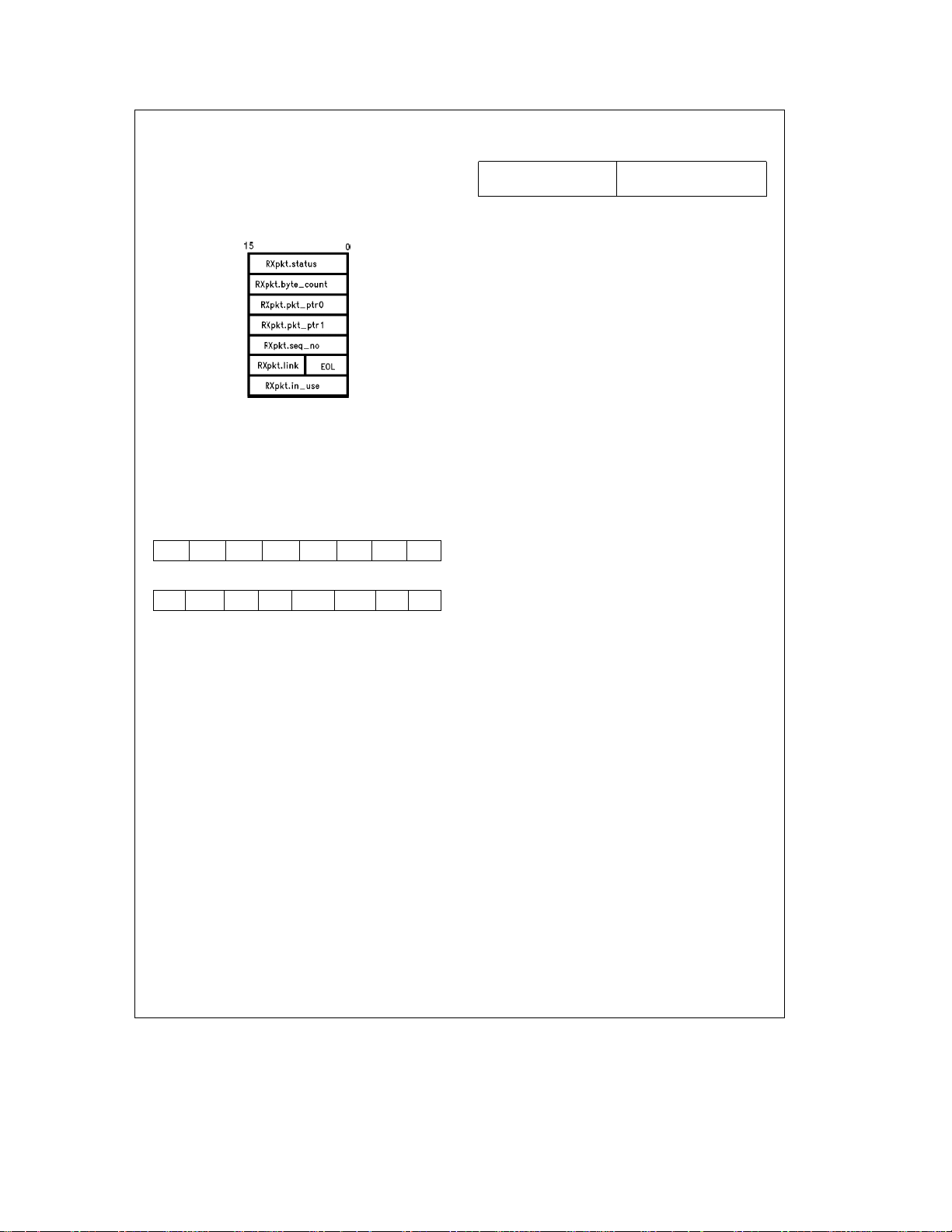
3.4.3 Receive Descriptor Area (RDA)
After the SONIC-16 buffers a packet to memory, it writes 5
words of status and control information into the RDA, reads
the link field to the next receive descriptor and writes to the
in use field of the current discriptor. Each receive descriptor
consists of the following sections (
FIGURE 3-5. Receive Descriptor Format
receive status: indicates status of the received packet. The
SONIC-16 writes the Receive Control register into this field.
Figure 3-6
shows the receive status format. This field is
loaded from the contents of the Receive Control register.
Note that ERR, RNT, BRD, PRO, and AMC are configuration bits and are programmed during initialization. See Section 4.3.3 for the description of the Receive Control register.
15 14 13 12 11 10 9 8
ERR RNT BRD PRO AMC LB1 LB0 MC
7654 3 2 10
BC LPKT CRS COL CRCR FAER LBK PRX
FIGURE 3-6. Receive Status Format
byte count: gives the length of the complete packet from
the start of Destination Address to the end of FCS.
packet pointer: a 23-bit pointer that locates the packet in
the RBA. The SONIC-16 writes the contents of the
CRBA0,1 registers into this field.
sequence numbers: this field displays the contents of two
8-bit counters (modulo 256) that sequence the RBAs used
and the packets buffered. These counters assist the system
in determining when an RBA has been completely processed. The sequence numbers allow the system to tally the
packets that have been processed within a particular RBA.
There are two sequence numbers that describe a packet:
the RBA Sequence Number and the Packet Sequence
Number. When a packet is buffered to memory, the SONIC16 maintains a single RBA Sequence Number for all packets in an RBA and sequences the Packet Number for succeeding packets in the RBA. When the SONIC-16 uses the
next RBA, it increments the RBA Sequence Number and
clears the Packet Sequence Number. The RBA’s sequence
counter is not incremented when the read RRA command is
issued in the Command register. The format of the Receive
Sequence Numbers are shown in
ters are reset during hardware reset or by writing zero to
them.
Figure 3-5
Figure 3-7
).
TL/F/11722– 14
. These coun-
15 8 7 0
RBA Sequence Number Packet Sequence Number
(Modulo 256) (Modulo 256)
FIGURE 3-7. Receive Sequence Number Format
receive link field: a 15-bit pointer (A15–A1) that locates
the next receive descriptor. The LSB of this field is the End
Of List (EOL) bit, and indicates the last descriptor in the list.
(Initialized by the system.)
in use field: this field provides a handshake between the
system and the SONIC-16 to indicate the ownership of the
descriptor. When the system avails a descriptor to the SONIC-16, it writes a non-zero value into this field. The SONIC16, in turn, sets this field to all ‘‘0’s’’ when it has finished
processing the descriptor. (That is, when the CRDA register
has advanced to the next receive descriptor.) Generally, the
SONIC-16 releases control after writing the status and control information into the RDA. If, however, the SONIC-16 has
reached the last descriptor in the list, it maintains ownership
of the descriptor until the system has appended additional
descriptors to the list. The SONIC-16 then relinquishes control after receiving the next packet. (See Section 3.4.6.1 for
details on when the SONIC-16 writes to this field.) The receive packet descriptor format is shown in
Figure 3-5
.
3.4.4 Receive Buffer Management Initialization
The Receive Resource, Descriptor, and Buffer areas (RRA,
RDA, RBA) in memory and the appropriate SONIC-16 registers must be properly initialized before the SONIC-16 begins
buffering packets. This section describes the initialization
process.
3.4.4.1 Initializing The Descriptor Page
All descriptor areas (RRA, RDA, and TDA) used by the
SONIC-16 reside within areas up to 32k (word) pages. This
page may be placed anywhere within the 23-bit address
range by loading the upper 8 address lines into the UTDA,
URDA, and URRA registers.
3.4.4.2 Initializing The RRA
The initialization of the RRA consists of loading the four
SONIC-16 RRA registers and writing the resource descriptor
information to memory.
The RRA registers are loaded with the following values.
Resource Start Area (RSA) register: The RSA is loaded
with the lower 16-bit address of the beginning of the RRA.
Resource End Area (REA) register: The REA is loaded
with the lower 16-bit address of the end of the RRA. The
end of the RRA is defined as the address of the last
RXrsrc.ptr0 field in the RRA plus 4 words (
Figure 3-3
).
Resource Read Pointer (RRP) register: The RRP is loaded with the lower 16-bit address of the first resource descriptor the SONIC-16 reads.
Resource Write Pointer (RWP) register: The RWP is loaded with the lower 16-bit address of the next vacant location
where a resource descriptor will be placed by the system.
Note: The RWP register must only point to either (1) the RXrsrc.ptr0 field of
one of the RRA Descriptors, (2) the memory address that the RSA
points to (the start of the RRA), or (3) the memory address that the
REA points to (the end of the RRA). When the RWP
son is made, it is performed after the complete RRA descriptor has
been read and not during the fetch. Failure to set the RWP to any of
the above values prevents the RWP
becoming true.
e
e
RRP compari-
RRP comparison from ever
17
Page 18
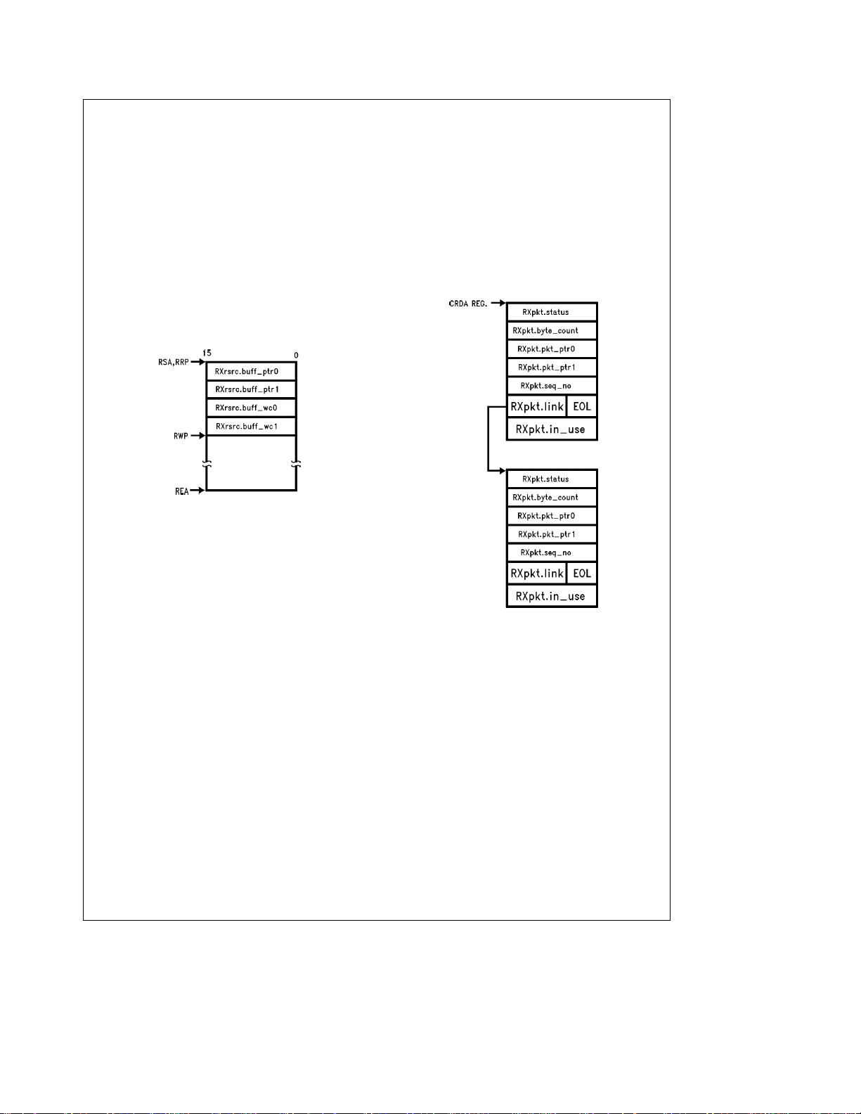
3.0 Buffer Management (Continued)
All RRA registers are concatenated with the URRA register
for generating the full 23-bit address.
The resource descriptors that the system writes to the RRA
consists of four fields: (1) RXrsrc.buffÐptr0, (2)
RXrsrc.buffÐptr1, (3) RXrsrc.buffÐwc0, and (4)
RXrsrc.buffÐwc1. The fields must be contiguous (they cannot straddle the end points) and are written in the order
shown in
denote the least and most significant portions for the Buffer
Pointer and Word Count. The first two fields supply the
23-bit starting location of the Receive Buffer Area (RBA),
and the second two define the number of 16-bit words that
the RBA occupies. Note that a restriction applies to the
Buffer Pointer and Word Count. The Buffer Pointer must be
pointing to a word boundary. Note also that the descriptors
must be properly aligned in the RRA as discussed in Section
3.3.
Figure 3-8
. The ‘‘0’’ and ‘‘1’’ in the descriptors
when it finishes using the descriptor. At startup, the Current
Receive Descriptor Address (CRDA) register must be loaded with the address of the first RXpkt.status field in order for
the SONIC-16 to begin receive processing at the first descriptor. An example of two descriptors linked together is
shown in
Figure 3-9
displayed in larger type. The other fields are written by the
SONIC-16 after a packet is accepted. The RXpkt.inÐuse
field is first written by the system, and then by the SONIC-
16. Note that the descriptors must be aligned properly as
discussed in section 3.3. Also note that the URDA register is
concatenated with the CRDA register to generate the full
23-bit address.
. The fields initialized by the system are
FIGURE 3-8. RRA Initialization
After configuring the RRA, the RRA Read command (setting
RRRA bit in the Command register) may be given. This
command causes the SONIC-16 to read the RRA descriptor
in a single block operation, and load the following registers
(see Section 4.2 for register mnemonics):
CRBA0 register
CRBA1 register
RBWC0 register
RBWC1 register
When the command has completed, the RRRA bit in the
Command register is reset to ‘‘0’’. Generally this command
is only issued during initialization. At all other times, the RRA
is automatically read as the SONIC-16 finishes using an
RBA.
3.4.4.3 Initializing The RDA
To accept multiple packets from the network, the receive
packet descriptors must be linked together via the
RXpkt.link fields. Each link field must be written with a 15-bit
(A15–A1) pointer to locate the beginning of the next descriptor in the list. The LSB of the RXpkt.link field is the End
of List (EOL) bit and is used to indicate the end of the descriptor list. EOL
the first or middle descriptors. The RXpkt.inÐuse field indicates whether the descriptor is owned by the SONIC-16.
The system writes a non-zero value to this field when the
descriptor is available, and the SONIC-16 writes all ‘‘0’s’’
w
RXrsrc.buffÐptr0
w
RXrsrc.buffÐptr1
w
RXrsrc.buffÐwc0
w
RXrsrc.buffÐwc1
e
1 for the last descriptor and EOLe0 for
TL/F/11722– 15
FIGURE 3-9. RDA Initialization Example
TL/F/11722– 16
3.4.4.4 Initializing the Lower Boundary of the RBA
A ‘‘false bottom’’ is set in the RBA by loading the End Of
Buffer Count (EOBC) register with a value equal to the maximum size packet in words (16 bits) that may be received.
This creates a lower boundary in the RBA. Whenever the
Remaining Buffer Word Count (RBWC0,1) registers decrement below the EOBC register, the SONIC-16 buffers the
next packet into another RBA. This also guarantees that a
packet is always contiguously buffered into a single Receive
Buffer Area (RBA). The SONIC-16 does not buffer a packet
into multiple RBAs.
After a hardware reset, the EOBC register is automatically
initialized to 2F8h (760 words or 1520 bytes).
Sometimes it may be desired to buffer a single packet per
RBA. When doing this, it is important to set EOBC and the
buffer size correctly. The suggested practice is to set EOBC
to a value that is at least 2 bytes less than the buffer size.
18
Page 19
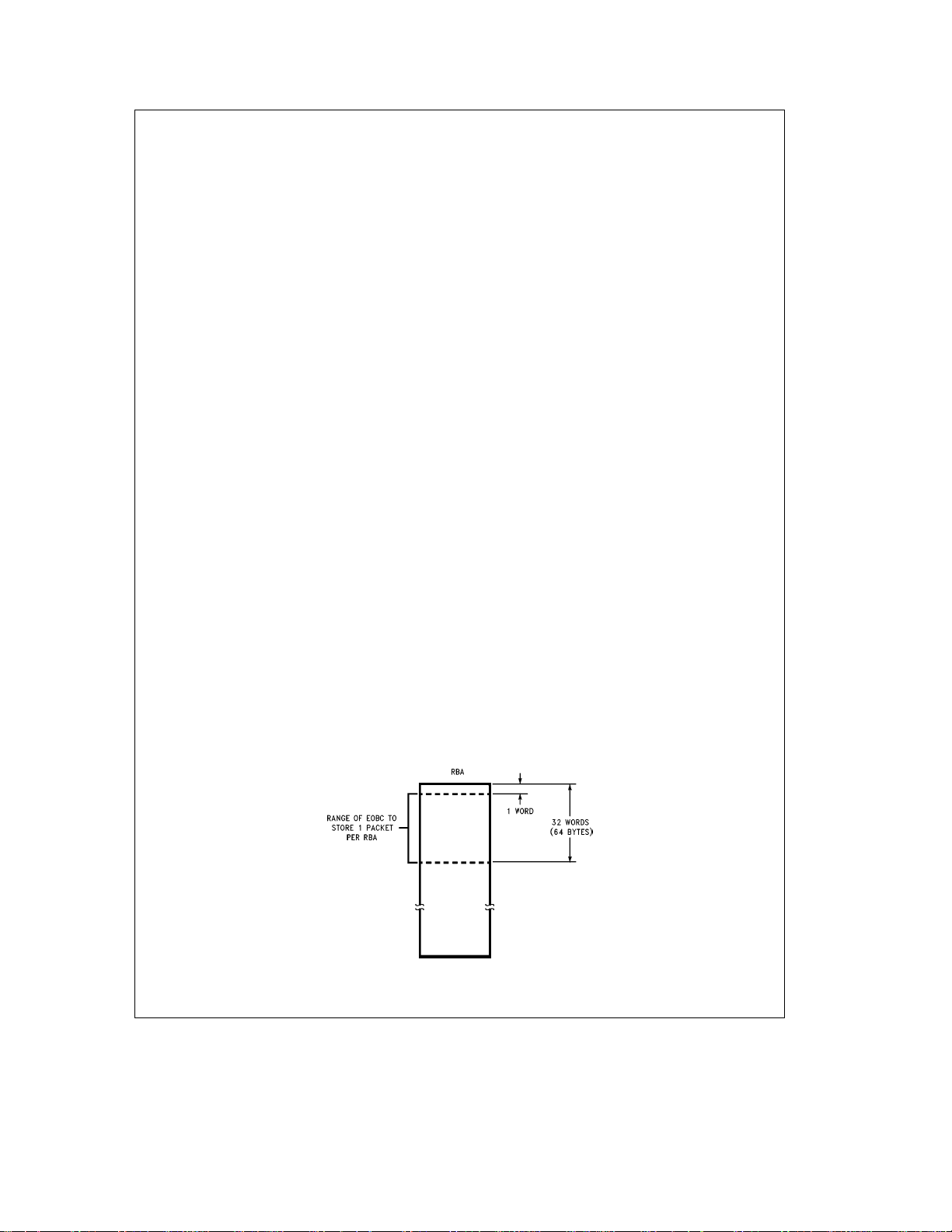
3.0 Buffer Management (Continued)
e
An example would be EOBC
the buffer size set to 760 words (1520 bytes). The buffer
can be any size, but as long as the EOBC is 1 word less
than the buffer size, only one packet will be buffered in that
RBA.
Note 1: It is possible to filter out most oversized packets by setting the buff-
er size to 759 words (1518 bytes). EOBC would be set to 758 words
(1516 bytes) for both cases. With this configuration, any packet over
1518 bytes, will not be completely buffered because the packet will
overflow the buffer. When a packet overflow occurs, a Receive Buffer Area Exceeded interrupt (RBAE in the Interrupt Status Register,
Section 4.3.6) will occur.
Note 2: When buffering one packet per buffer, it is suggested that the val-
ues in Note 1 above be used. Since the minimum legal sized Ethernet packet is 64 bytes, however, it is possible to set EOBC as much
as 64 bytes less than the buffer size and still end up with one packet
Figure 3-10
per buffer.
3.4.5 Beginning of Reception
At the beginning of reception, the SONIC-16 checks its internally stored EOL bit from the previous RXpkt.link field for
a ‘‘1’’. If the SONIC-16 finds EOL
the previous reception, there were no more remaining receive packet descriptors. It re-reads the same RXpkt.link
field to check if the system has updated this field since the
last reception. If the SONIC-16 still finds EOL
ceases. (See Section 3.5 for adding descriptors to the list.)
Otherwise, the SONIC-16 begins storing the packet in the
RBA starting at the Current Receive Buffer Address
(CRBA0,1) registers and continues until the packet has
completed. Concurrent with the packet reception, the Remaining Buffer Word Count (RBWC0,1) registers are decremented after each word is written to memory. This register
determines the remaining words in the RBA at the end of
reception.
3.4.6 End of Packet Processing
At the end of a reception, the SONIC-16 enters its end of
packet processing sequence to determine whether to accept or reject the packet based on receive errors and packet size. At the end of reception the SONIC-16 enters one of
the following two sequences:
Ð Successful reception sequence
Ð Buffer recovery for runt packets or packets with errors
759 words (1518 bytes) and
shows this ‘‘range.’’
e
1, it recognizes that after
e
1, reception
3.4.6.1 Successful Reception
If the SONIC-16 accepts the packet, it first writes 5 words of
descriptor information in the RDA beginning at the address
pointed to by the Current Receive Descriptor Address
(CRDA) register. It then reads the RXpkt.link field to advance the CRDA register to the next receive descriptor. The
SONIC-16 also checks the EOL bit for a ‘‘1’’ in this field. If
e
EOL
1, no more descriptors are available for the SONIC-
16. The SONIC-16 recovers the address of the current
RXpkt.link field (from a temporary register) and generates a
‘‘Receive Descriptors Exhausted’’ indication in the Interrupt
Status register. (See Section 3.4.7 on how to add descriptors.) The SONIC-16 maintains ownership of the descriptor
by
not
writing to the RXpkt.inÐuse field. Otherwise, if
e
EOL
0, the SONIC-16 advances the CRDA register to the
next descriptor and resets the RXpkt.inÐuse field to all
‘‘0’s’’.
The SONIC-16 accesses the complete 7 word RDA descriptor in a single block operation.
The SONIC-16 also checks if there is remaining space in the
RBA. The SONIC-16 compares the Remaining Buffer Word
Count (RBWC0,1) registers with the static End Of Buffer
Count (EOBC). If the RBWC is less than the EOBC, a maximum sized packet will no longer fit in the remaining space in
the RBA; hence, the SONIC-16 fetches a resource descriptor from the RRA and loads its registers with the pointer and
word count of the next available RBA.
3.4.6.2 Buffer Recovery for Runt Packets or
Packets with Errors
If a runt packet (less than 64 bytes) or packet with errors
arrives and the Receive Control register has been configured to not accept these packets, the SONIC-16 recovers
its pointers back to the original positions. The CRBA0,1 registers are not advanced and the RBWC0,1 registers are not
decremented. The SONIC-16 recovers its pointers by maintaining a copy of the buffer address in the Temporary Receive Buffer Address registers (TRBA0,1). The SONIC-16
recovers the value in the RBWC0,1 registers from the Temporary Buffer Word Count registers (TBWC0,1).
3.4.7 Overflow Conditions
When an overflow condition occurs, the SONIC-16 halts its
DMA operations to prevent writing into unauthorized memory. The SONIC-16 uses the Interrupt Status register (ISR) to
indicate three possible overflow conditions that can occur
Range of EOBCe(RXrsrc.wc0,1b2 to RXrsrc.wc0,1b32)
FIGURE 3-10. Setting EOBC for Single Packet RBA
19
TL/F/11722– 17
Page 20
3.0 Buffer Management (Continued)
when its receive resources have been exhausted. The system should respond by replenishing the resources that have
been exhausted. These overflow conditions (Descriptor Resources Exhausted, Buffer Resources Exhausted, and RBA
Limit Exceeded) are indicated in the Interrupt Status register
and are detailed as follows:
Descriptor Resources Exhausted: This occurs when the
SONIC-16 has reached the last receive descriptor in the list,
meaning that the SONIC-16 has detected EOL
tem must supply additional descriptors for continued reception. The system can do this in one of two ways: 1) appending descriptors to the existing list, or 2) creating a separate
list.
1) Appending descriptors to the existing list. This is the easiest and preferred way. To do this, the system, after creating the new list, joins the new list to the existing list by
simply writing the beginning address of the new list into
the RXpkt.link field and setting EOL
reception, the SONIC-16 re-reads the last RXpkt.link
field, and updates its CRDA register to point to the next
descriptor.
2) Creating a separate list. This requires an additional step
because the lists are not joined together and requires
that the CRDA register be loaded with the address of the
RXpkt.link field in the new list.
During this overflow condition, the SONIC-16 maintains
ownership of the descriptor (RXpkt.inÐuse
waits for the system to add additional descriptors to the list.
When the system appends more descriptors, the SONIC-16
releases ownership of the descriptor after writing 0000h to
the RXpkt.inÐuse field.
Buffer Resources Exhausted: This occurs when the
SONIC-16 has detected that the Resource Read Pointer
(RRP) and Resource Write Pointer (RWP) registers are
equal (i.e., all RRA descriptors have been exhausted). The
RBE bit in the Interrupt Status register is set when the SONIC-16 finishes using the second to last receive buffer and
reads the last RRA descriptor. Actually, the SONIC-16 is not
truly out of resources, but gives the system an early warning
of an impending out of resources condition. To continue
reception after the last RBA is used, the system must supply
additional RRA descriptor(s), update the RWP register, and
clear the RBE bit in the ISR. The SONIC-16 rereads the
RRA after this bit is cleared.
RBA Limit Exceeded: This occurs when a packet does not
completely fit within the remaining space of the RBA. This
can occur if the EOBC register is not programmed to a value
greater than the largest packet that can be received. When
this situation occurs, the packet is truncated and the SONIC-16 reads the RRA to obtain another RBA. Indication of
an RBA limit being exceeded is signified by the Receive
Buffer Area Exceeded (RBAE) interrrupt being set (see section 4.3.6). An RDA will not be set up for the truncated packet and the buffer space will not be re-used. To rectify this
potential overflow condition, the EOBC register must be
loaded with a value equal to or greater than the largest
packet that can be accepted. See Section 3.4.2.
3.5 TRANSMIT BUFFER MANAGEMENT
To begin transmission, the system software issues the
Transmit command (TXP
e
1 in the CR). The Transmit Buffer Management uses two areas in memory for transmitting
packets
(Figure 3-11),
the Transmit Descriptor Area (TDA)
e
1. The sys-
e
0. At the next
i
00h) and
and the Transmit Buffer Area (TBA). During transmission,
the SONIC-16 fetches control information from the TDA,
loads its appropriate registers, and then transmits the data
from the TBA. When the transmission is complete, the SONIC-16 writes the status information in the TDA. From a single
transmit command, packets can either be transmitted singly
or in groups if several descriptors have been linked together.
FIGURE 3-11. Overview of Transmit Buffer Management
TL/F/11722– 18
3.5.1 Transmit Descriptor Area (TDA)
The TDA contains descriptors that the system has generated to exchange status and control information. Each descriptor corresponds to a single packet and consists of the
following 16-bit fields.
TXpkt.status: This field is written by the SONIC-16 and provides status of the transmitted packet. See Section 3.5.1.2
for more details.
TXpkt.config: This field allows programming the SONIC-16
to one of the various transmit modes. The SONIC-16 reads
this field and loads the corresponding configuration bits
(PINTR, POWC, CRCI, and EXDIS) into the Transmit Control
register. See Section 3.5.1.1 for more details.
TXpkt.pktÐsize: This field contains the byte count of the
entire packet
TXpkt.fragÐcount: This field contains the number of fragments the packet is segmented into.
TXpkt.fragÐptr0,1: This field contains a 23-bit pointer
which locates the packet fragment to be transmitted in the
Transmit Buffer Area (TBA). This pointer is not restricted to
any byte alignment.
TXpkt.fragÐsize: This field contains the byte count of the
packet fragment. The minimum fragment size is 1 byte.
TXpkt.link: This field contains a 15-bit pointer (A15 –A1) to
the next TDA descriptor. The LSB, the End Of List (EOL) bit,
indicates the last descriptor in the list when set to a ‘‘1’’.
When descriptors have been linked together, the SONIC-16
transmits back-to-back packets from a single transmit command.
The data of the packet does not need to be contiguous, but
can exist in several locations (fragments) in memory. In this
case, the TXpkt.fragÐcount field is greater than one, and
additional TXpkt.fragÐptr0,1 and TXpkt.fragÐsize fields
corresponding to each fragment are used. The descriptor
format is shown in
Figure 3-12.
20
Page 21
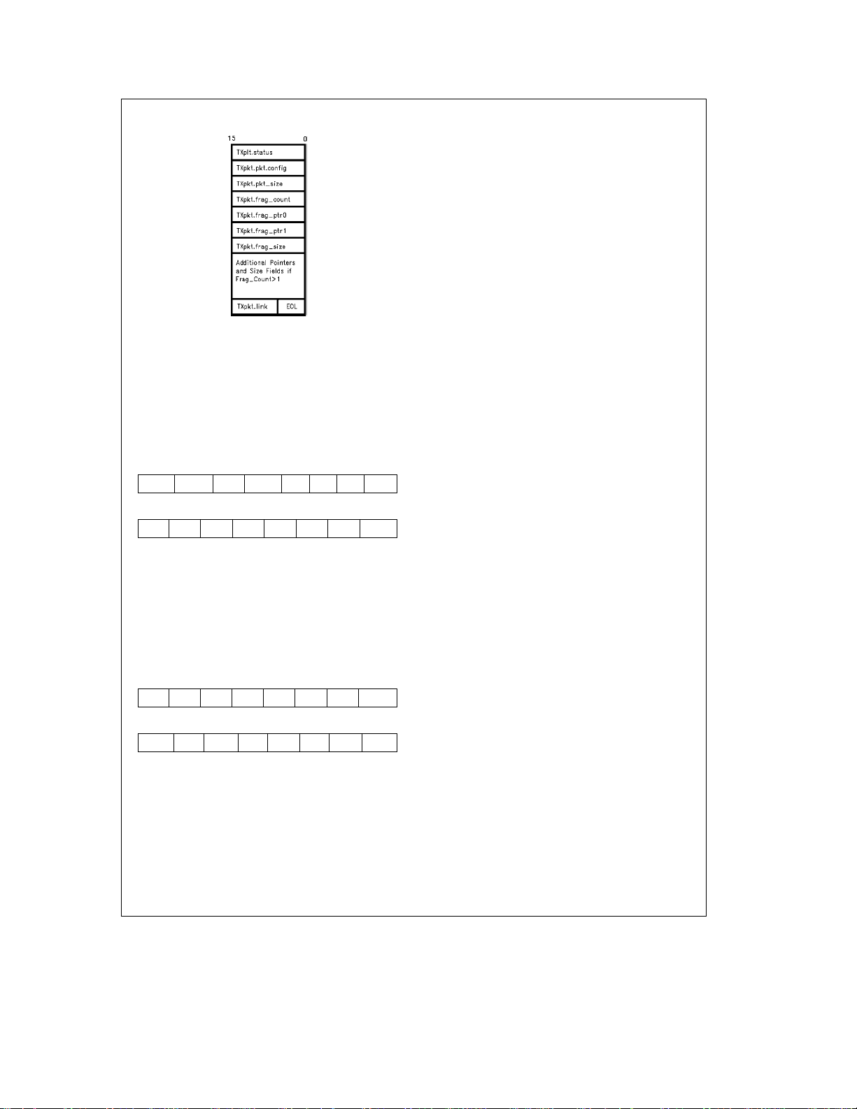
3.0 Buffer Management (Continued)
FIGURE 3-12. Transmit Descriptor Area
3.5.1.1 Transmit Configuration
The TXpkt.config field allows the SONIC-16 to be programmed into one of the transmit modes before each transmission. At the beginning of each transmission, the SONIC16 reads this field and loads the PINTR, POWC, CRCI, and
EXDIS bits into the Transmit Control register (TCR). The
configuration bits in the TCR correspond directly with the
bits in the TXpkt.config field as shown in
Section 4.3.4 for the description on the TCR.
15 14 13 12 11 10 9 8
PINTR POWC CRCI EXDIS X X X X
7654321 0
XXXXXXX X
Note: xedon’t care
3.5.1.2 Transmit Status
At the end of each transmission the SONIC-16 writes the
status bits (
and the number of collisions experienced during the transmission into the TXpkt.status field
served). Bits NC4-NC0 indicate the number of collisions
where NC4 is the MSB. See Section 4.3.4 for the description of the TCR.
15 14 13 12 11 10 9 8
NC4 NC3 NC2 NC1 NC0 EXD DEF NCRS
CRSL EXC OWC res PMB FU BCM PTX
3.5.2 Transmit Buffer Area (TBA)
The TBA contains the fragments of packets that are defined
by the descriptors in the TDA. A packet can consist of a
single fragment or several fragments, depending upon the
fragment count in the TDA descriptor. The fragments also
can reside anywhere within the full 23-bit address range,
and be aligned to any byte boundary. When an odd byte
boundary is given, the SONIC-16 automatically begins reading data at the corresponding word boundary. The SONIC16 ignores the extraneous bytes which are written into the
FIGURE 3-13. TXpkt.config Field
k
10:0l) of the Transmit Control Register (TCR)
76543210
FIGURE 3-14. TXpkt.status Field
TL/F/11722– 19
Figure 3-13.
(Figure 3-14
See
, resere-
FIFO during odd byte alignment fragments. The minimum
allowed fragment size is 1 byte.
tionship between the TDA and the TBA for single and multifragmented packets.
3.5.3 Preparing To Transmit
All fields in the TDA descriptor and the Current Transmit
Descriptor Address (CTDA) register of the SONIC-16 must
be initialized before the Transmit Command (setting the
TXP bit in the Command register) can be issued. If more
than one packet is queued, the descriptors must be linked
together with the TXpkt.link field. The last descriptor must
have EOL
To begin transmission, the system loads the address of the
first TXpkt.status field into the CTDA register. Note that the
upper 8-bits of address are loaded in the Upper Transmit
Descriptor (UTDA) register. The user performs the following
transmit initialization.
1) Initialize the TDA
2) Load the CTDA register with the address of the first
3) Issue the transmit command
Note that if the Source Address of the packet being transmitted is not in the CAM, the Packet Monitored Bad (PMB)
bit in the TXpxt.status field will be set (see Section 4.3.4).
3.5.3.1 Transmit Process
When the Transmit Command (TXP
register) is issued, the SONIC-16 fetches the control information in the TDA descriptor, loads its appropriate registers
(shown below) and begins transmission. (See Section 4.2
for register mnemonics.)
TCR
TPS
TFC
TSA0
TSA1
TFS
CTDA
(CTDA is loaded after all fragments have been read and
successfully transmitted. If the halt transmit command is issued (HTX bit in the Command register is set) the CTDA
register is not loaded.)
During transmission, the SONIC-16 reads the packet descriptor in the TDA and transmits the data from the TBA. If
TXpkt.fragÐcount is greater than one, the SONIC-16, after
finishing transmission of the fragment, fetches the next
TXpkt.fragÐptr0,1 and TXpkt.fragÐsize fields and transmits
the next fragment. This process continues until all fragments of a packet are transmitted. At the end of packet
transmission, status is written in to the TXpkt.status field.
The SONIC-16 then reads the TXpkt.link field and checks if
EOL
scriptor and transmits the next packet. If EOL
IC-16 generates a ‘‘Transmission Done’’ indication in the
Interrupt Status register and resets the TXP bit in the Command register.
In the event of a collision, the SONIC-16 recovers its pointer
in the TDA and retransmits the packet up to 15 times. The
SONIC-16 maintains a copy of the CTDA register in the
Temporary Transmit Descriptor Address (TTDA) register.
The SONIC-16 performs a block operation of 6, 3, or 2 accesses in the TDA, depending on where the SONIC-16 is in
the transmit process. For the first fragment, it reads the
e
1 and all other descriptors must have EOLe0.
transmit descriptor
w
TXpkt.config
w
TXpkt.pktÐsize
w
TXpkt.fragÐcount
w
TXpkt.fragÐptr0
w
TXpkt.fragÐptr1
w
TXpkt.fragÐsize
w
TXpkt.link
e
0. If it is ‘‘0’’, the SONIC-16 fetches the next de-
Figure
3-11 shows the rela-
e
1 in the Command
e
1 the SON-
21
Page 22
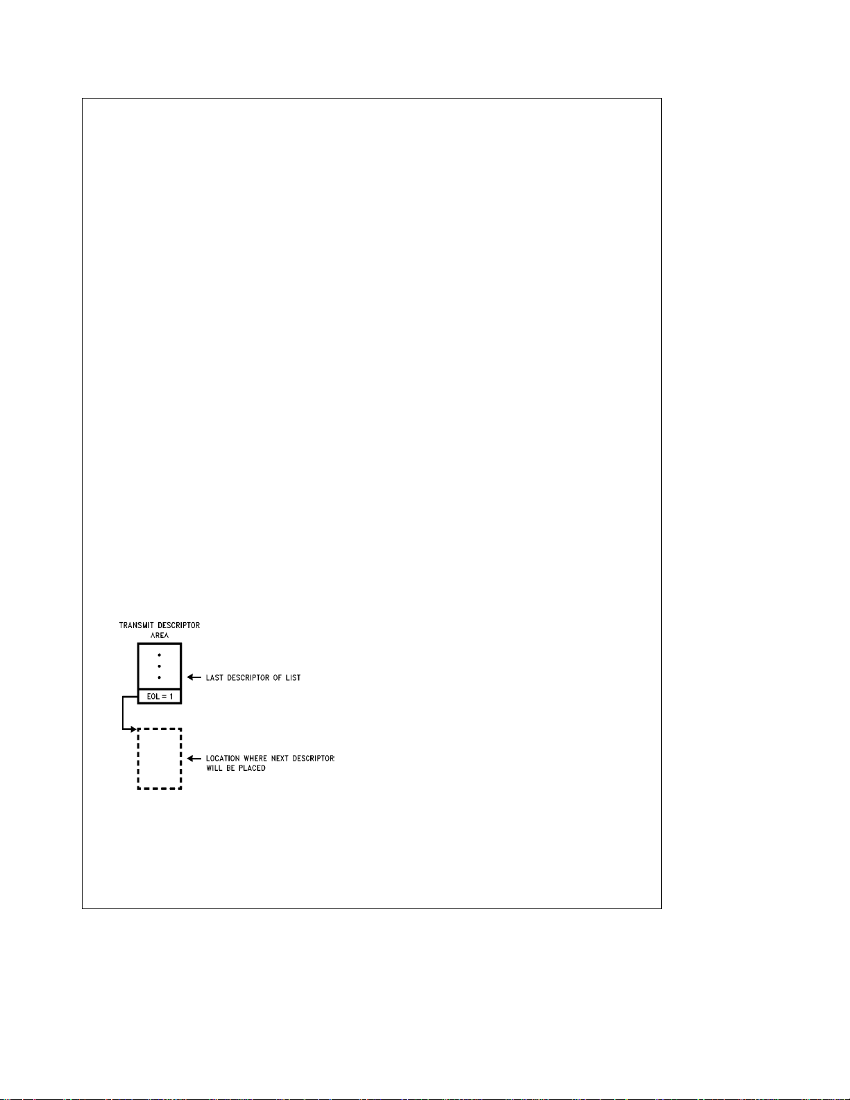
3.0 Buffer Management (Continued)
TXpkt.config to TXpkt.fragÐsize (6 accesses). For the next
fragment, if any, it reads the next 3 fields from TXpkt.frag
ptr0 to TXpkt.fragÐsize (3 accesses). At the end of transmission it writes the status information to TXpkt.status and
reads the TXpkt.link field (2 accesses).
3.5.3.2 Transmit Completion
The SONIC-16 stops transmitting under two conditions. In
the normal case, the SONIC-16 transmits the complete list
of descriptors in the TDA and stops after it detects EOL
1. In the second case, certain transmit errors cause the
SONIC-16 to abort transmission. If
Count Mismatch, Excessive Collision,
(if enabled) errors occur, transmission ceases. The CTDA
register points to the last packet transmitted. The system
can also halt transmission under software control by setting
the HTX bit in the Command register. Transmission halts
after the SONIC-16 writes to the TXpkt.status field.
3.5.4 Dynamically Adding TDA Descriptors
Descriptors can be dynamically added during transmission
without halting the SONIC-16. The SONIC-16 can also be
guaranteed to transmit the complete list including newly appended descriptors (barring any transmit abort conditions)
by observing the following rule: The last TXpkt.link field
must point to the next location where a descriptor will be
added (see step 3 below and
for appending descriptors consists of:
1. Creating a new descriptor with its TXpkt.link pointing to
the next vacant descriptor location and its EOL bit set to
a ‘‘1’’.
2. Resetting the EOL bit to a ‘‘0’’ of the previously last de-
scriptor.
3. Re-issuing the Transmit command (setting the TXP bit in
the Command register).
Step 3 assures that the SONIC-16 will transmit all the packets in the list. If the SONIC-16 is currently transmitting, the
Transmit command has no effect and continues transmitting
until it detects EOL
e
1. If the SONIC-16 had just finished
transmitting, it continues transmitting from where it had previously stopped.
FIGURE 3-15. Initializing Last Link Field
FIFO Underrun, Byte
or
Excessive Deferral
Figure 3-15
). The procedure
TL/F/11722– 20
4.0 SONIC-16 Registers
The SONIC-16 contains two sets of registers: The status/
Ð
e
control registers and the CAM memory cells. The status/
control registers are used to configure, control, and monitor
SONIC-16 operation. They are directly addressable registers and occupy 64 consecutive address locations in the
system memory space (selected by the RA5 – RA0 address
pins). There are a total of 64 status/control registers divided
into the following categories:
User Registers: These registers are accessed by the user
to configure, control, and monitor SONIC-16 operation.
These are the only SONIC-16 registers the user needs to
access.
Figure 4-3
shows the programmer’s model and Ta-
ble 4-1 lists the attributes of each register.
Internal Use Registers: These registers (Table 4-2) are
used by the SONIC-16 during normal operation and are not
intended to be accessed by the user.
National Factory Test Registers: These registers (Table
4-3) are for National factory use only and should never be
accessed by the user. Accessing these registers during normal operation can cause improper functioning of the
SONIC-16.
4.1 THE CAM UNIT
The CAM unit memory cells are indirectly accessed by programming the CAM descriptor area in system memory and
issuing the LCAM command (setting the LCAM bit in the
Control register). The CAM cells do not occupy address locations in register space and, thus, are not accessible
through the RA5–RA0 address pins. The CAM control registers, however, are part of the user register set and must be
initialized before issuing the LCAM command (see Section
4.3.10).
The Content Addressable Memory (CAM) consists of sixteen 48-bit entries for complete address filtering
(Figure 4-1)
of network packets. Each entry corresponds to a 48-bit destination address that is user programmable and can contain
any combination of Multicast or Physical addresses. Each
entry is partitioned into three 16-bit CAM cells accessible
through CAM Address Ports (CAP 2, CAP 1 and CAP 0) with
CAP0 corresponding to the least significant 16 bits of the
Destination Address and CAP2 corresponding to the most
significant bits. The CAM is accessed in a two step process.
First, the CAM Entry Pointer is loaded to point to one of the
16 entries. Then, each of the CAM Address Ports is accessed to select the CAM cell. The 16 user programmable
CAM entries can be masked out with the CAM Enable register (see section 4.3.10).
Note: It is not necessary to program a broadcast address into the CAM
when it is desired to accept broadcast packets. Instead, to accept
broadcast packets, set the BRD bit in the Receive Control register. If
the BRD bit has been set, the CAM is still active. This means that it is
possible to accept broadcast packets at the same time as accepting
packets that match physical addresses in the CAM.
4.1.1 The Load CAM Command
Because the SONIC-16 uses the CAM for a relatively long
period of time during reception, it can only be written to via
the CAM Descriptor Area (CDA) and is only readable when
22
Page 23
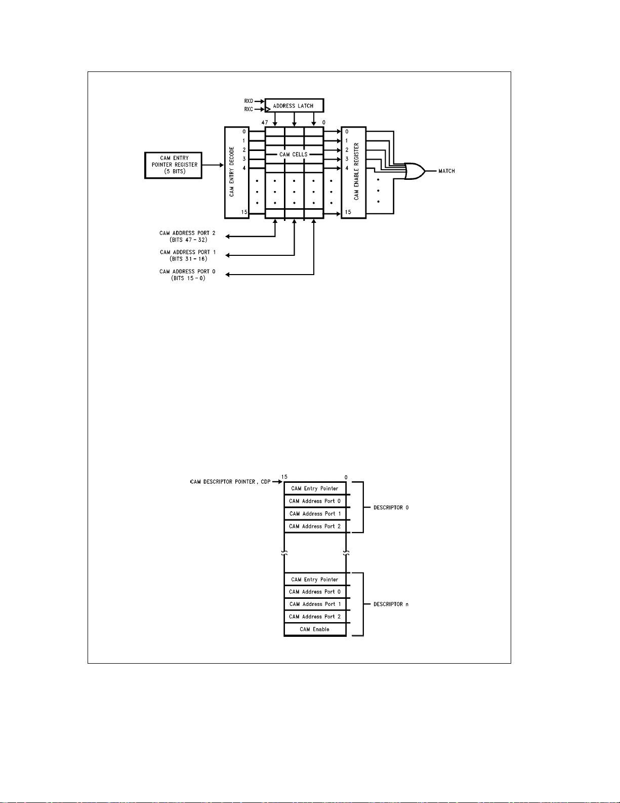
4.0 SONIC-16 Registers (Continued)
FIGURE 4-1. CAM Organization
the SONIC-16 is in software reset. The CDA resides in the
same 64k byte block of memory as the Receive Resource
Area (RRA) and contains descriptors for loading the CAM
registers. These descriptors are contiguous and each descriptor consists of four 16-bit fields
field contains the value to be loaded into the CAM Entry
Pointer and the remaining fields are for the three CAM Address Ports (see Section 4.3.10). In addition, there is one
more field after the last descriptor containing the mask for
the CAM Enable register. Each of the CAM descriptors are
addressed by the CAM Descriptor Pointer (CDP) register.
After the system has initialized the CDA, it can issue the
Load CAM command to program the SONIC-16 to read the
CDA and load the CAM. The procedure for issuing the Load
CAM command is as follows.
1. Initialize the Upper Receive Resource Address (URRA)
register. Note that the CAM Descriptor Area must reside
within the same 64k page as the Receive Resource
Area. (See Section 4.3.9).
(Figure 4-2).
The first
TL/F/11722– 21
2. Initialize the CDA as described above.
3. Initialize the CAM Descriptor Count with the number of
CAM descriptors. Note, only the lower 5 bits are used in
this register. The other bits are don’t cares. (See Section
4.3.10).
4. Initialize the CAM Descriptor Pointer to locate the first
descriptor in the CDA. This register must be reloaded
each time a new Load CAM command is issued.
5. Issue the Load CAM command (LCAM) in the Command
register. (See Section 4.3.1).
If a transmission or reception is in progress, the CAM DMA
function will not occur until these operations are complete.
When the SONIC-16 completes the Load CAM command,
the CDP register points to the next location after the CAM
Enable field and the CDC equals zero. The SONIC-16 resets
the LCAM bit in the Command register and sets the Load
CAM Done (LCD) bit in the ISR.
FIGURE 4-2. CAM Descriptor Area Format
23
TL/F/11722– 22
Page 24
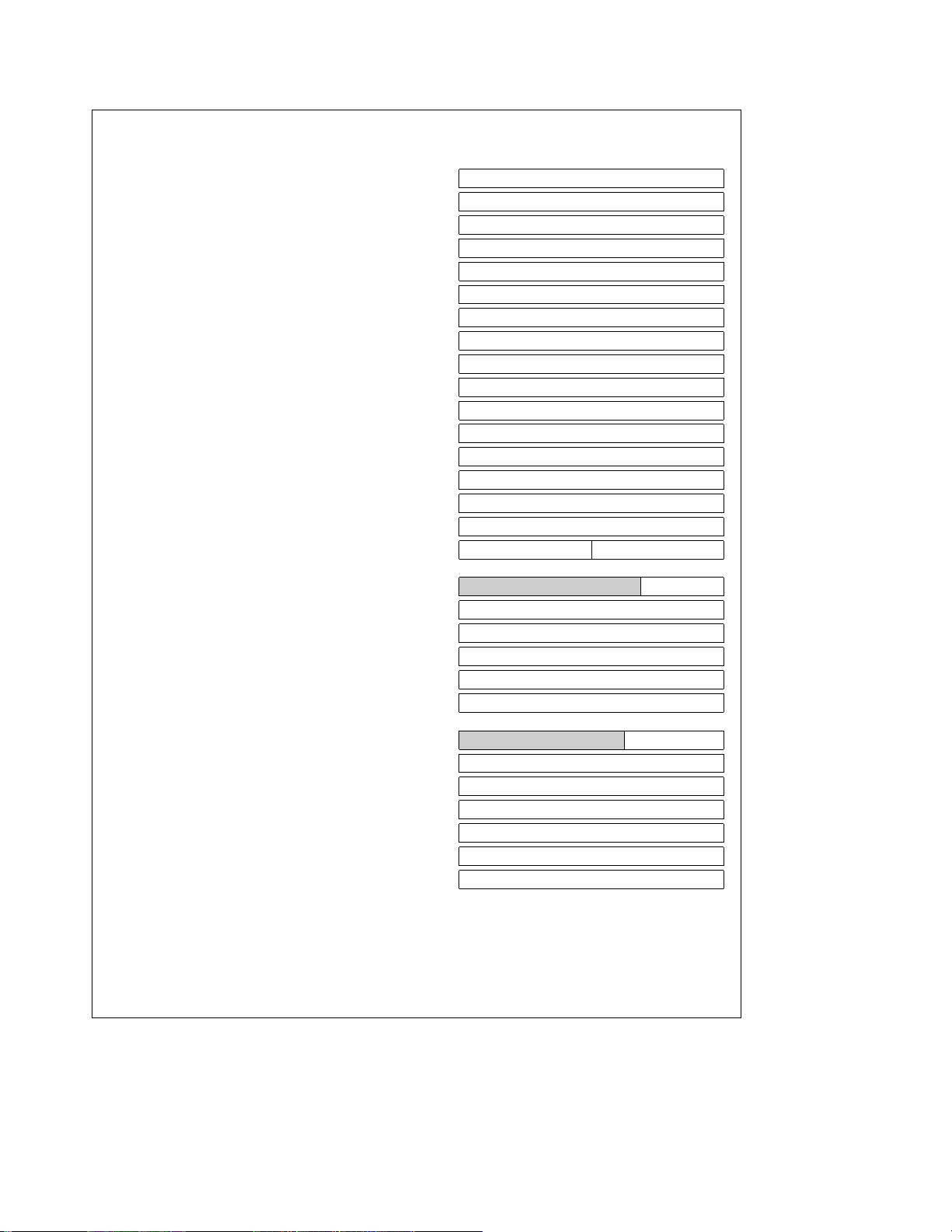
4.0 SONIC-16 Registers (Continued)
k
l
5:0
RA
0h Command Register Status and Control Fields
1 Data Configuration Register Control Fields
Status and
Control Registers
Transmit
Registers
Receive
Registers
CAM
Registers
2 Receive Control Register Status and Control Fields
3 Transmit Control Register Status and Control Fields
4 Interrupt Mask Register Mask Fields
5 Interrupt Status Register Status Fields
$
3F Data Configuration Register 2 Control Fields
6 Upper Transmit Descriptor Address Register Upper 16-bit Address Base
7 Current Transmit Descriptor Address Register Lower 16-bit Address Offset
Ð
0D Upper Receive Descriptor Address Register Upper 16-bit Address Base
0E Current Receive Descriptor Address Register Lower 16-bit Address Offset
14 Upper Receive Resource Address Register Upper 16-bit Address Base
15 Resource Start Address Register Lower 16-bit Address Offset
16 Resource End Address Register Lower 16-bit Address Offset
17 Resource Read Register Lower 16-Bit Address Offset
18 Resource Write Register Lower 16-bit Address Offset
2B Receive Sequence Counter Count Value 8 7 Count Value
$
21 CAM Entry Pointer Pointer
22 CAM Address Port 2 Most Significant 16 bits of CAM Entry
23 CAM Address Port 1 Middle 16 bits of CAM Entry
24 CAM Address Port 0 Least Significant 16 bits of CAM Entry
25 CAM Enable Register Mask Fields
26 CAM Descriptor Pointer Lower 16-bit Address Offset
$27 CAM Descriptor Count Count Value
Tally
Counters
Watchdog
Timer
2C CRC Error Tally Counter Count Value
2D Frame Alignment Error Tally Count Value
)
2E Missed Packet Tally Count Value
29 Watchdog Timer 0 Lower 16-bit Count Value
2A Watchdog Timer 1 Upper 16-bit Count Value
Ð
28 Silicon Revision Register Chip Revision Number
FIGURE 4-3. Register Programming Model
15 0
4
5
24
Page 25

4.0 SONIC-16 Registers (Continued)
4.2 STATUS/CONTROL REGISTERS
This set of registers is used to convey status/control information to/from the host system and to control the operation
of the SONIC-16. These registers are used for loading commands generated from the system, indicating transmit and
receive status, buffering data to/from memory, and provid-
TABLE 4-1. User Registers
RA5–RA0 Access Register Symbol
COMMAND AND STATUS REGISTERS
00h R/W Command CR 4.3.1
01 (Note 3) R/W Data Configuration DCR 4.3.2
02 R/W Receive Control RCR 4.3.3
03 R/W Transmit Control TCR 4.3.4
04 R/W Interrupt Mask IMR 4.3.5
05 R/W Interrupt Status ISR 4.3.6
3F (Note 3) R/W Data Configuration 2 DCR2 4.3.7
TRANSMIT REGISTERS
06 R/W Upper Transmit Descriptor Address UTDA 4.3.8, 3.4.4.1
07 R/W Current Transmit Descriptor Address CTDA 4.3.8, 3.5.3
RECEIVE REGISTERS
0D R/W Upper Receive Descriptor Address URDA 4.3.9, 3.4.4.1
0E R/W Current Receive Descriptor Address CRDA 4.3.9, 3.4.4.3
13 R/W End of Buffer Word Count EOBC 4.3.9, 3.4.2
14 R/W Upper Receive Resource Address URRA 4.3.9, 3.4.4.1
15 R/W Resource Start Address RSA 4.3.9, 3.4.1
16 R/W Resource End Address REA 4.3.9, 3.4.1
17 R/W Resource Read Pointer RRP 4.3.9, 3.4.1
18 R/W Resource Write Pointer RWP 4.3.9, 3.4.1
2B R/W Receive Sequence Counter RSC 4.3.9, 3.4.3.2
CAM REGISTERS
21 R/W CAM Entry Pointer CEP 4.1, 4.3.10
22 (Note 1) R CAM Address Port 2 CAP2 4.1, 4.3.10
23 (Note 1) R CAM Address Port 1 CAP1 4.1, 4.3.10
24 (Note 1) R CAM Address Port 0 CAP0 4.1, 4.3.10
25 (Note 2) R/W CAM Enable CE 4.1, 4.3.10
26 R/W CAM Descriptor Pointer CDP 4.1, 4.3.10
27 R/W CAM Descriptor Count CDC 4.1, 4.3.10
TALLY COUNTERS
2C (Note 4) R/W CRC Error Tally CRCT 4.3.11
2D (Note 4) R/W FAE Tally FAET 4.3.11
2E (Note 4) R/W Missed Packet Tally MPT 4.3.11
ing interrupt control. The registers are selected by asserting
chip select to the SONIC-16 and providing the necessary
address on register address pins RA5–RA0. Tables 4-1,
4-2, and 4-3 show the locations of all SONIC-16 registers
and where information on the registers can be found in the
data sheet.
Description
(section)
25
Page 26
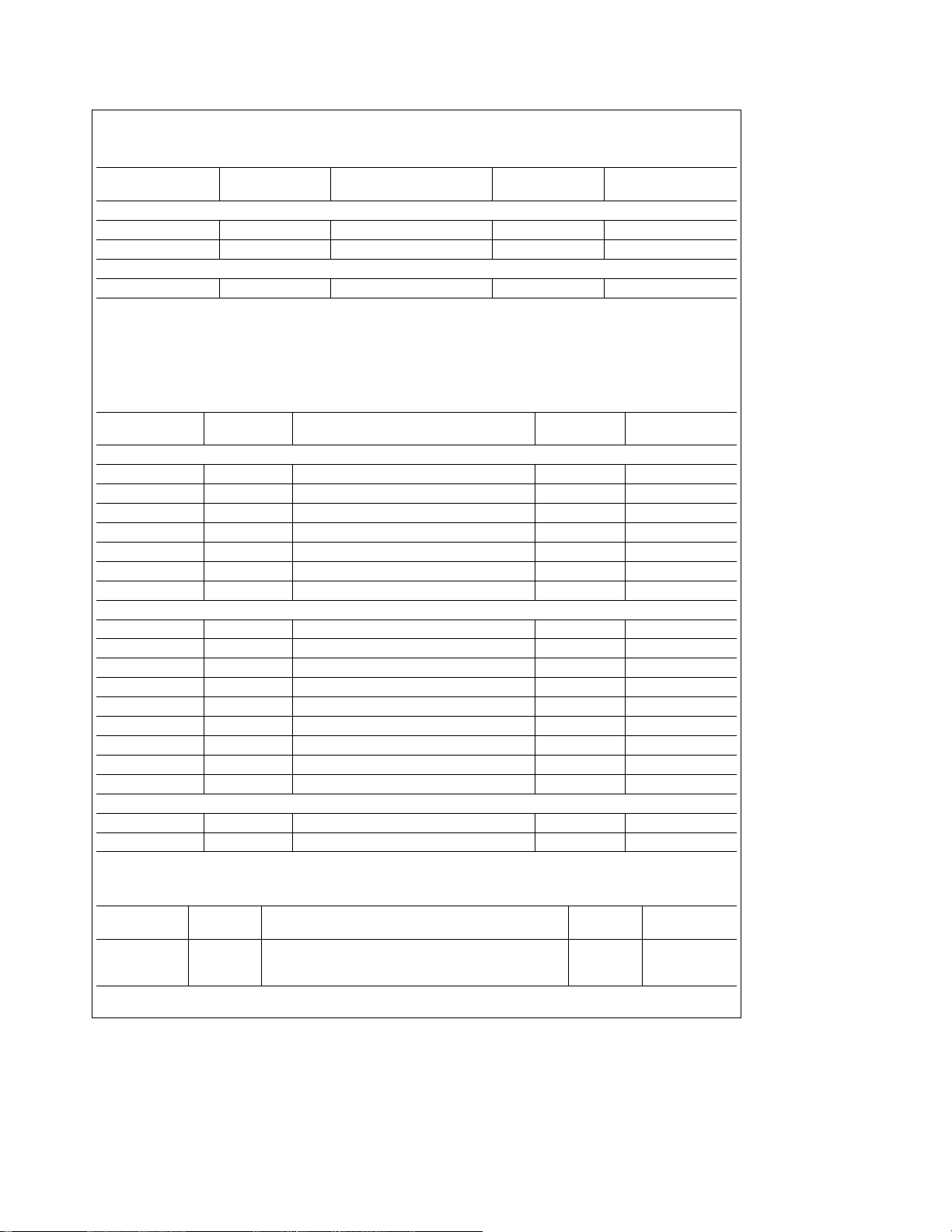
4.0 SONIC-16 Registers (Continued)
TABLE 4-1. User Registers (Continued)
RA5–RA0 Access Register Symbol
WATCHDOG COUNTERS
29 R/W Watchdog Timer 0 WT0 4.3.12
2A R/W Watchdog Timer 1 WT1 4.3.12
SILICON REVISION
28 R Silicon Revision SR 4.3.13
Note 1: These registers can only be read when the SONIC-16 is in reset mode (RST bit in the CR is set). The SONIC-16 gives invalid data when these registers are
read in non-reset mode.
Note 2: This register can only be written to when the SONIC-16 is in reset mode. This register is normally only loaded by the Load CAM command.
Note 3: The Data Configuration registers, DCR and DCR2, can only be written to when the SONIC-16 is in reset mode (RST bit in CR is set). Writing to these
registers while not in reset mode does not alter the registers.
Note 4: The data written to these registers is inverted before being latched. That is, if a value of FFFFh is written, these registers will contain and read back the
value of 0000h. Data is not inverted during a read operation.
TABLE 4-2. Internal Use Registers (Users should not write to these registers)
(RA5–RA0) Access Register Symbol
TRANSMIT REGISTERS
08 (Note 1) R/W Transmit Packet Size TPS 3.5
09 R/W Transmit Fragment Count TFC 3.5
0A R/W Transmit Start Address 0 TSA0 3.5
0B R/W Transmit Start Address 1 TSA1 3.5
0C (Note 2) R/W Transmit Fragment Size TFS 3.5
20 R/W Temporary Transmit Descriptor Address TTDA 3.5.4
2F R Maximum Deferral Timer MDT 4.3.4
RECEIVE REGISTERS
0F R/W Current Receive Buffer Address 0 CRBA0 3.4.2, 3.4.4.2
10 R/W Current Receive Buffer Address 1 CRBA1 3.4.2, 3.4.4.2
11 R/W Remaining Buffer Word Count 0 RBWC0 3.4.2, 3.4.4.2
12 R/W Remaining Buffer Word Count 1 RBWC1 3.4.2, 3.4.4.2
19 R/W Temporary Receive Buffer Address 0 TRBA0 3.4.6.2
1A R/W Temporary Receive Buffer Address 1 TRBA1 3.4.6.2
1B R/W Temporary Buffer Word Count 0 TBWC0 3.4.6.2
1C R/W Temporary Buffer Word Count 1 TBWC1 3.4.6.2
1F R/W Last Link Field Address LLFA none
ADDRESS GENERATORS
1D R/W Address Generator 0 ADDR0 none
1E R/W Address Generator 1 ADDR1 none
Note 1: The data that is read from these registers is the inversion of what has been written to them.
Note 2: The value that is written to this register is shifted once.
TABLE 4-3. National Factory Test Registers
(RA5–RA0) Access Register Symbol
30 These registers are for factory use only. Users must not
#
R/W address these registers or improper SONIC-16 operation none none
3E can occur.
Description
(section)
Description
(section)
Description
(section)
26
Page 27

4.0 SONIC-16 Registers (Continued)
4.3 REGISTER DESCRIPTION
4.3.1 Command Register
k
l
(RA
This register
sponding bits for the function. For all bits, except for the RST bit, the SONIC-16 resets the bit after the command is completed.
With the exception of RST, writing a ‘‘0’’ to any bit has no effect. Before any commands can be issued, the RST bit must first be
reset to ‘‘0’’. This means that, if the RST bit is set, two writes to the Command Register are required to issue a command to the
SONIC-16; one to clear the RST bit, and one to issue the command.
This register also controls the general purpose 32-bit Watchdog Timer. After the Watchdog Timer register has been loaded, it
begins to decrement once the ST bit has been set to ‘‘1’’. An interrupt is issued when the count reaches zero if the Timer
Complete interrupt is enabled in the IMR.
During hardware reset, bits 7, 4, and 2 are set to a ‘‘1’’; all others are cleared. During software reset bits 9, 8, 1, and 0 are
cleared and bits 7 and 2 are set to a ‘‘1’’; all others are unaffected.
e
5:0
0h)
(Figure 4-4
) is used for issuing commands to the SONIC-16. These commands are issued by setting the corre-
15141312111098765432 10
000000LCAM RRRA RST 0 ST STP RXEN RXDIS TXP HTX
r/w r/w r/w r/w r/w r/w r/w r/w r/w
reread only, r/weread/write
FIGURE 4-4. Command Register
Field Meaning
LCAM LOAD CAM
RRRA READ RRA
RST SOFTWARE RESET
ST START TIMER
STP STOP TIMER
RXEN RECEIVER ENABLE
RXDIS RECEIVER DISABLE
TXP TRANSMIT PACKET(S)
HTX HALT TRANSMISSION
Bit Description
15–10 Must be 0
9 LCAM: LOAD CAM
Setting this bit causes the SONIC-16 to load the CAM with the descriptor that is pointed to by the CAM Descriptor
Pointer register.
Note: This bit must not be set during transmission (TXP is set). The SONIC-16 will lock up if both bits are set simultaneously.
8 RRRA: READ RRA
Setting this bit causes the SONIC-16 to read the next RRA descriptor pointed to by the Resource Read Pointer
(RRP) register. Generally this bit is only set during initialization. Setting this bit during normal operation can cause
improper receive operation.
7 RST: SOFTWARE RESET
Setting this bit resets all internal state machines. The CRC generator is disabled and the Tally counters are halted,
but not cleared. The SONIC-16 becomes operational when this bit is reset to ‘‘0’’. A hardware reset sets this bit to a
‘‘1’’. It must be reset to ‘‘0’’ before the SONIC-16 becomes operational.
6 Must be 0.
5 ST: START TIMER
Setting this bit enables the general-purpose watchdog timer to begin counting or to resume counting after it has
been halted. This bit is reset when the timer is halted (i.e., STP is set). Setting this bit resets STP.
4 STP: STOP TIMER
Setting this bit halts the general-purpose watchdog timer and resets the ST bit. The timer resumes when the ST bit is
set. This bit powers up as a ‘‘1’’. Note: Simultaneously setting bits ST and STP stops the timer.
27
Page 28

4.0 SONIC-16 Registers (Continued)
4.3 REGISTER DESCRIPTION
4.3.1 Command Register (Continued)
k
l
(RA
Bit Description
3 RXEN: RECEIVER ENABLE
2 RXDIS: RECEIVER DISABLE
1 TXP: TRANSMIT PACKET(S)
0 HTX: HALT TRANSMISSION
e
5:0
0h)
Setting this bit enables the receive buffer management engine to begin buffering data to memory. Setting this bit
resets the RXDIS bit. Note: If this bit is set while the MAC unit is currently receiving a packet, both RXEN and RXDIS
are set until the network goes inactive (i.e., the SONIC-16 will not start buffering in the middle of a packet being
received).
Setting this bit disables the receiver from buffering data to memory or the Receive FIFO. If this bit is set during the
reception of a packet, the receiver is disabled only after the packet is processed. The RXEN bit is reset when the
receiver is disabled. Tally counters remain active regardless of the state of this bit. Note: If this bit is set while the
SONIC-16 is currently receiving a packet, both RXEN and RXDIS are set until the packet is fully received.
Setting this bit causes the SONIC-16 to transmit packets which have been set up in the Transmit Descriptor Area
(TDA). The SONIC-16 loads its appropriate registers from the TDA, then begins transmission. The SONIC-16 clears
this bit after any of the following conditions have occurred: (1) transmission had completed (i.e., after the SONIC-16
has detected EOL
has occurred. This condition occurs when any of the following bits in the TCR have been set: EXC, EXD, FU, or BCM.
Note: This bit must not be set if a Load CAM operation is in progress (LCAM is set). The SONIC-16 will lock up if
both bits are set simultaneously.
Setting this bit halts the transmit command after the current transmission has completed. TXP is reset after
transmission has halted. The Current Transmit Descriptor Address (CTDA) register points to the last descriptor
transmitted. The SONIC-16 samples this bit after writing to the TXpkt.status field.
e
1), (2) the Halt Transmission command (HTX) has taken effect, or (3) a transmit abort condition
28
Page 29
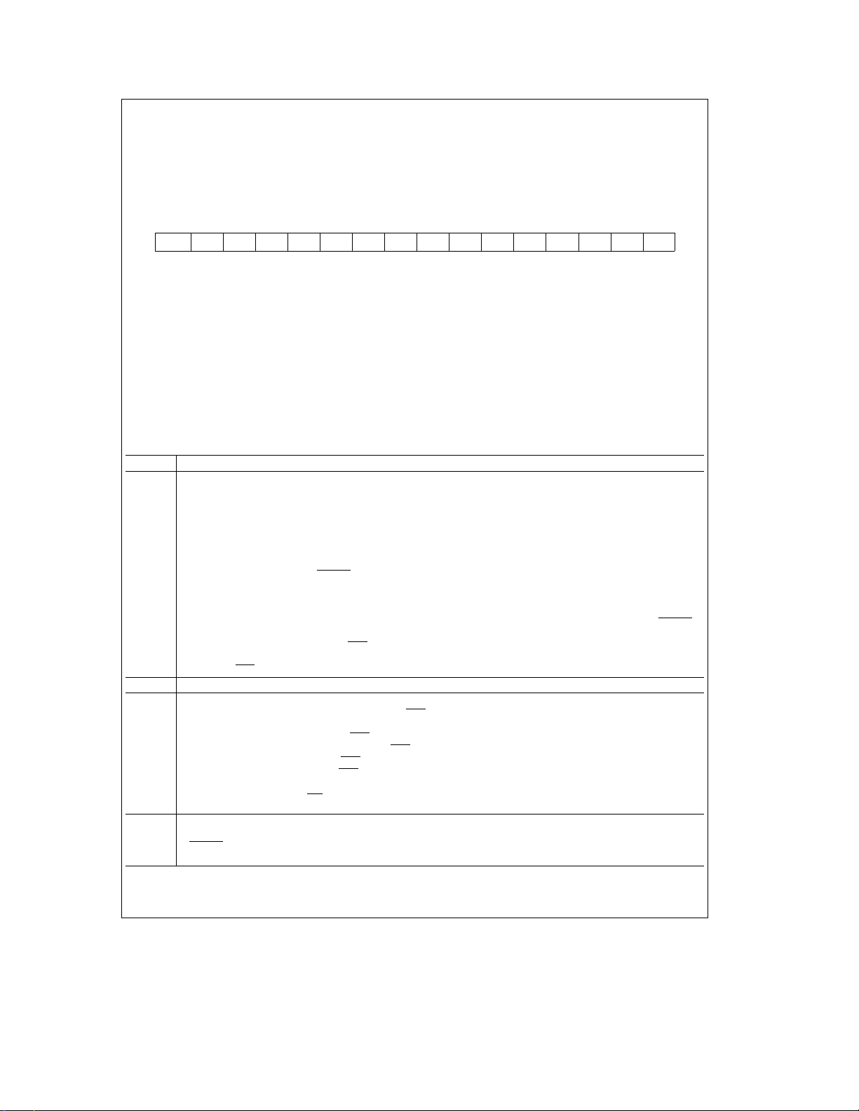
4.0 SONIC-16 Registers (Continued)
4.3.2 Data Configuration Register
k
l
(RA
This register
During a hardware reset, bits 15 and 13 are cleared; all other bits are unaffected. (Because of this, the first thing the driver
software does to the SONIC-16 should be to set up this register.) All bits are unaffected by a software reset. This register must
only be accessed when the SONIC-16 is in reset mode (i.e., the RST bit is set in the Command register).
Bit Description
15 EXBUS: EXTENDED BUS MODE
14 Must be 0.
13 LBR: LATCHED BUS RETRY
12, 11 PO1, PO0: PROGRAMMABLE OUTPUTS
e
5:0
1h)
(Figure 4-5)
establishes the bus cycle options for reading/writing data to/from 16- or 32-bit memory systems.
1514131211109876543210
EXBUS 0 LBR PO1 PO0 SBUS USR1 USR0 WC1 WC0 0 BMS RFT1 RFT0 TFT1 TFT0
r/w r/w r/w r/w r/w r/w r/w r/w r/w r/w r/w r/w r/w r/w
r/weread/write
FIGURE 4-5. Data Configuration Register
Field Meaning
EXBUS EXTENDED BUS MODE
LBR LATCHED BUS RETRY
PO0,PO1 PROGRAMMABLE OUTPUTS
SBUS SYNCHRONOUS BUS MODE
USR0, USR1 USER DEFINABLE PINS
WC0, WC1 WAIT STATE CONTROL
DW DATA WIDTH SELECT
BMS BLOCK MODE SELECT FOR DMA
RFT0, RFT1 RECEIVE FIFO THRESHOLD
TFT0, TFT1 TRANSMIT FIFO THRESHOLD
Setting this bit enables the Extended Bus mode which enables the following:
1) Extended Programmable Outputs, EXUSR
external ENDEC interface into four programmable user outputs, EXUSR
k
USR
1:0l. These outputs are programed with bits 15-12 in the DCR2 (see Section 4.3.7). On hardware reset,
these four pins will be TRI-STATE
k
3:0l: This changes the TXD, LBK, RXC and RXD pins from the
and will remain that way until the DCR is changed. If EXBUS is enabled, then
É
k
3:0lrespectively, which are similar to
these pins will remain TRI-STATE until the SONIC-16 becomes a bus master, at which time they will be driven
according to the DCR2. If EXBUS is disabled, then these four pins work normally as external ENDEC interface pins.
2) Synchronous Termination, STERM
synchronous memory termination input for compatibility with Motorola style processors. This input is only useful
when Asynchronous Bus mode is selected (bit 10 below is set to ‘‘0’’) and BMODE
: This changes the TXC pin from the External ENDEC interface into a
e
1 (Motorola mode). On
hardware reset, this pin will be TRI-STATE and will remain that way until the DCR is changed. If EXBUS is enabled,
this pin will remain TRI-STATE until the SONIC-16 becomes a bus master, at which time it will become the STERM
input. If EXBUS is disabled, then this pin works normally as the TXC pin for the external ENDEC interface.
3) Asynchronous Bus Retry: Causes BRT
to be clocked in asynchronously off the falling edge of bus clock. This only
applies, however, when the SONIC-16 is operating in asynchronous mode (bit 10 below is set to ‘‘0’’). If EXBUS is
not set, BRT
The LBR bit controls the mode of operation of the BRT
is sampled synchronously off the rising edge of bus clock. (See Section 5.4.6.)
signal (see pin description). It allows the BUS Retry operation
to be latched or unlatched.
0: Unlatched mode: The assertion of BRT
The SONIC-16 will retry the operation when BRT
forces the SONIC-16 to finish the current DMA operation and get off the bus.
is deserted.
1: Latched mode: The assertion of BRT forces the SONIC-16 to finish the current DMA operation as above, however,
the SONIC-16 will not retry until BRT
is deasserted and the BR bit in the ISR (see Section 4.3.6) has been reset.
Hence, the mode has been latched on until the BR bit is cleared.
Note: Unless LBR is set to a ‘‘1’’, BRT must remain asserted at least until the SONIC-16 has gone idle. See Section 5.4.6 and the timing for Bus
Retry in Section 7.0.
The PO1,PO0 bits individually control the USR1,0 pins respectively when SONIC-16 is a bus master (HLDA or
BGACK
is active). When PO1/PO0 are set to a 1 the USR1/USR0 pins are high during bus master operations and
when these bits are set to a 0 the USR1/USR0 pins are low during bus master operations.
29
Page 30

4.0 SONIC-16 Registers (Continued)
4.3.2 Data Configuration Register (Continued)
k
l
(RA
Bit Description
10 SBUS: SYNCHRONOUS BUS MODE
9, 8 USR1,0: USER DEFINABLE PINS
7, 6 WC1,0: WAIT STATE CONTROL
5MUST BE 0.
4 BMS: BLOCK MODE SELECT FOR DMA
3, 2 RFT1,RFT0: RECEIVE FIFO THRESHOLD
1, 0 TFT1,TFT0: TRANSMIT FIFO THRESHOLD
e
5:0
1h)
The SBUS bit is used to select the mode of system bus operation when SONIC-16 is a bus master. This bit selects
the internal ready line to be either a synchronous or asynchronous input to SONIC-16 during block transfer DMA
operations.
0: Asynchronous mode. RDYi
(BMODEe0) or DSACK0,1 (BMODEe1) are respectively internally synchronized
at the falling edge of the bus clock (T2 of the DMA cycle). No setup or hold times need to be met with
respect to this edge to guarantee proper bus operation.
1: Synchronous mode. RDYi
(BMODEe0) and DSACK0,1 (BMODEe1) must respectively meet the setup and
hold times with respect to the rising edge of T1 or T2 to guarantee proper bus operation.
The USR1,0 bits report the level of the USR1,0 signal pins, respectively, after a chip hardware reset. If the USR1,0
signal pins are at a logical 1 (tied to V
are at a logical 0 (tied to ground) during a hardware reset the USR1,0 bits are set to a 0. These bits are latched on
) during a hardware reset the USR1,0 bits are set to a 1. If the USR1,0 pins
CC
the rising edge of RST. Once set they remain set/reset until the next hardware reset.
These encoded bits determine the number of additional bus cycles (T2 states) that are added during each DMA
cycle.
WC1 WC0 Bus Cycles Added
00 0
01 1
10 2
11 3
Determines how data is emptied or filled into the Receive or Transmit FIFO.
0: Empty/fill mode: All DMA transfers continue until either the Receive FIFO has emptied or the Transmit FIFO has
filled completely.
1: Block mode: All DMA transfers continue until the programmed number of bytes (RFT0, RFT1 during reception or
TF0, TF1 during transmission) have been transferred. (See note for TFT0, TFT1.)
These encoded bits determine the number of words (or long words) that are written into the receive FIFO from the
MAC unit before a receive DMA request occurs. (See Section 1.4.)
RFT1 RFT0 Threshold
0 0 2 words (4 bytes)
0 1 4 words (8 bytes)
1 0 8 words (16 bytes)
1 1 12 words (24 bytes)
Note: In block mode (BMS bite1), the receive FIFO threshold sets the number of words (or long words) written to memory during a receive DMA
block cycle.
These encoded bits determine the minimum number of words (or long words) the DMA section maintains in the
transmit FIFO. A bus request occurs when the number of words drops below the transmit FIFO threshold. (See
Section 1.4.)
TFT1 TFT0 Threshold
0 0 4 words (8 bytes)
0 1 8 words (16 bytes)
1 0 12 words (24 bytes)
1 1 14 words (28 bytes)
Note: In block mode (BMSe1), the number of bytes the SONIC-16 reads in a single DMA burst equals the transmit FIFO threshold value. If the
number of words or long words needed to fill the FIFO is less than the threshold value, then only the number of reads required to fill the FIFO in a
single DMA burst will be made. Typically, with the FIFO threshold value set to 12 or 14 words, the number of memory reads needed is less than the
FIFO threshold value.
30
Page 31

4.0 SONIC-16 Registers (Continued)
4.3.3 Receive Control Register
k
l
(RA
This register is used to filter incoming packets and provide status information of accepted packets
bits 15 – 11 to a ‘‘1’’ enables the corresponding receive filter. If none of these bits are set, only packets which match the CAM
Address registers are accepted. Bits 10 and 9 control the loopback operations.
After reception, bits 8 –0 indicate status information about the accepted packet and are set to ‘‘1’’ when the corresponding
condition is true. If the packet is accepted, all bits in the RCR are written into the RXpkt.status field. Bits 8 – 6 and 3 – 0 are
cleared at the reception of the next packet.
This register is unaffected by a software reset.
e
5:0
2h)
(Figure 4-6).
Setting any of
15 14 13 12 11 10 9 8 7 6 5 4 3 2 1 0
ERR RNT BRD PRO AMC LB1 LB0 MC BC LPKT CRS COL CRCR FAER LBK PRX
r/w r/w r/w r/w r/w r/w r/w r r r r r r r r r
reread only, r/weread/write
FIGURE 4-6. Receive Control Register
Field Meaning
ERR ACCEPT PACKET WITH ERRORS
RNT ACCEPT RUNT PACKETS
BRD ACCEPT BROADCAST PACKETS
PRO PHYSICAL PROMISCUOUS PACKETS
AMC ACCEPT ALL MULTICAST PACKETS
LB0,LB1 LOOPBACK CONTROL
MC MULTICAST PACKET RECEIVED
BC BROADCAST PACKET RECEIVED
LPKT LAST PACKET IN RBA
CRS CARRIER SENSE ACTIVITY
COL COLLISION ACTIVITY
CRCR CRC ERROR
FAER FRAME ALIGNMENT ERROR
LBK LOOPBACK PACKET RECEIVED
PRX PACKET RECEIVED OK
Bit Description
15 ERR: ACCEPT PACKET WITH CRC ERRORS OR COLLISIONS
0: Reject all packets with CRC errors or when a collision occurs.
1: Accept packets with CRC errors and ignore collisions.
14 RNT: ACCEPT RUNT PACKETS
0: Normal address match mode.
1: Accept runt packets (packets less than 64 bytes in length).
Note: A hardware reset clears this bit.
13 BRD: ACCEPT BROADCAST PACKETS
0: Normal address match mode.
1: Accept broadcast packets (packets with addresses that match the CAM are also accepted).
Note: This bit is cleared upon hardware reset.
12 PRO: PHYSICAL PROMISCUOUS MODE
Enable all Physical Address packets to be accepted.
0: Normal address match mode.
1: Promiscuous mode.
11 AMC: ACCEPT ALL MULTICAST PACKETS
0: Normal address match mode.
1: Enables all multicast packets to be accepted. Broadcast packets are also accepted regardless
of the BRD bit. (Broadcast packets are a subset of multicast packets.)
31
Page 32

4.0 SONIC-16 Registers (Continued)
4.3.3 Receive Control Register (Continued)
k
l
(RA
Bit Description
10, 9 LB1,LB0: LOOPBACK CONTROL
8 MC: MULTICAST PACKET RECEIVED
7 BC: BROADCAST PACKET RECEIVED
6 LPKT: LAST PACKET IN RBA
5 CRS: CARRIER SENSE ACTIVITY
4 COL: COLLISION ACTIVITY
3 CRCR: CRC ERROR
2 FAER: FRAME ALIGNMENT ERROR
1 LBK: LOOPBACK PACKET RECEIVED
0 PRX: PACKET RECEIVED OK
e
5:0
2h)
These encoded bits control loopback operations for MAC loopback, ENDEC loopback and Transceiver lookback. For
proper operation, the CAM Address registers and Receive Control register must be initialized to accept the Destination
address of the loopback packet (see Section 1.7).
Note: A hardware reset clears these bits.
LB1 LB0 Function
0 0 No loopback, normal operation
0 1 MAC loopback
1 0 ENDEC loopback
1 1 Transceiver loopback
This bit is set when a packet is received with a Multicast Address.
This bit is set when a packet is received with a Broadcast Address.
This bit is set when the last packet is buffered into a Receive Buffer Area (RBA). The SONIC-16 detects this condition
when its Remaining Buffer Word Count (RBWC0,1) register is less than the End Of Buffer Count (EOBC) register. (See
Section 3.4.2.)
Set when CRS is active. Indicates the presence of network activity.
Indicates that the packet received had a collision occur during reception.
Indicates the packet contains a CRC error. If the packet also contains a Frame Alignment error, FAER will be set
instead (see below).
Indicates that the incoming packet was not correctly framed on an 8-bit boundary. Note: if no CRC errors have
occurred, this bit is not set (i.e., this bit is only set when both a frame alignment and CRC errors occur).
Indicates that the SONIC-16 has successfully received a loopback packet.
Indicates that a packet has been received without CRC, frame alignment, length (runt packet) errors or collisions.
32
Page 33

4.0 SONIC-16 Registers (Continued)
4.3.4 Transmit Control Register
k
l
(RA
This register is used to program the SONIC-16’s transmit actions and provide status information after a packet has been
transmitted
TCR to configure the various transmit modes (see section 3.5.1.1). When the transmission ends, bits 10 – 0 indicate status
information and are set to a ‘‘1’’ when the corresponding condition is true. These bits, along with the number of collisions
information, are written into the TXpkt.status field at the end of transmission (see section 3.5.1.2). Bits 9 and 5 are cleared after
the TXpkt.status field has been written. Bits 10, 7, 6, and 1 are cleared at the commencement of the next transmission while bit 8
is set at this time.
A hardware reset sets bits 8 and 1 to a ‘‘1’’. This register is unaffected by a software reset.
e
5:0
3h)
(Figure 4-7).
At the beginning of transmission, bits 15, 14, 13 and 12 from the TXpkt.config field are loaded into the
15 14 13 12 11 10 9 8 7 6 5 4 3 2 1 0
PINTR POWC CRCI EXDIS 0 EXD DEF NCRS CRSL EXC OWC 0 PMB FU BCM PTX
r/w r/w r/w r/w r r r r r r r r r r
reread only, r/weread/write
FIGURE 4-7. Transmit Control Register
Field Meaning
PINTR PROGRAMMABLE INTERRUPT
POWC PROGRAMMED OUT OF WINDOW COLLISION TIMER
CRCI CRC INHIBIT
EXDIS DISABLE EXCESSIVE DEFERAL TIMER
EXD EXCESSIVE DEFERRAL
DEF DEFERRED TRANSMISSION
NCRS NO CRS
CRSL CRS LOST
EXC EXCESSIVE COLLISIONS
OWC OUT OF WINDOW COLLISION
PMB PACKET MONITORED BAD
FU FIFO UNDERRUN
BCM BYTE COUNT MISMATCH
PTX PACKET TRANSMITTED OK
Bit Description
15 PINTR: PROGRAMMABLE INTERRUPT
This bit allows transmit interrupts to be generated under software control. The SONIC-16 will issue an interrupt (PINT
in the Interrupt Status Register) immediately after reading a TDA and detecting that PINTR is set in the TXpkt.config
field.
Note: In order for PINTR to operate properly, it must be set and reset in the TXpkt.config field by alternating TDAs. This is necessary because after
PINT has been issued in the ISR, PINTR in the Transmit Control Register must be cleared before it is set again in order to have the interrupt issued
for another packet. The only effective way to do this is to set PINTR toa1nomore often than every other packet.
14 POWC: PROGRAM ‘‘OUT OF WINDOW COLLISION’’ TIMER
This bit programs when the out of window collision timer begins.
0: timer begins after the Start of Frame Delimiter (SFD).
1: timer begins after the first bit of preamble.
13 CRCI: CRC INHIBIT
0: transmit packet with 4-byte FCS field
1: transmit packet without 4-byte FCS field
12 EXDIS: DISABLE EXCESSIVE DEFERRAL TIMER:
0: excessive deferral timer enabled
1: excessive deferral timer disabled
11 Must be 0.
10 EXD: EXCESSIVE DEFERRAL
Indicates that the SONIC-16 has been deferring for 3.2 ms. The transmission is aborted if the excessive deferral
timer is enabled (i.e. EXDIS is reset). This bit can only be set if the excessive deferral timer is enabled.
33
Page 34

4.0 SONIC-16 Registers (Continued)
4.3.4 Transmit Control Register (Continued)
k
l
(RA
Bit Description
9 DEF: DEFERRED TRANSMISSION
8 NCRS: NO CRS
7 CRSL: CRS LOST
6 EXC: EXCESSIVE COLLISIONS
5 OWC: OUT OF WINDOW COLLISION
4 Must be 0.
3 PMB: PACKET MONITORED BAD
2 FU: FIFO UNDERRUN
1 BCM: BYTE COUNT MISMATCH
0 PTX: PACKET TRANSMITTED OK
e
5:0
3h)
Indicates that the SONIC-16 has deferred its transmission during the first attempt. If subsequent collisions occur, this
bit is reset. This bit is cleared after the TXpkt.status field is written in the TDA.
Indicates that Carrier Sense (CRS) was not present during transmission. CRS is monitored from the beginning of the
Start of Frame Delimiter to the last byte transmitted. The transmission will not be aborted. This bit is set at the start
of preamble and is reset if CRS is detected. Hence, if CRS is never detected throughout the entire transmission of
the packet, this bit will remain set.
Note: NCRS will always remain set in MAC loopback.
Indicates that CRS has gone low or has not been present during transmission. CRS is monitored from the beginning
of the Start of Frame Delimiter to the last byte transmitted. The transmission will not be aborted.
Note: if CRS was never present, both NCRS and CRSL will be set simultaneously. Also, CRSL will always be set in MAC loopback.
Indicates that 16 collisions have occurred. The transmission is aborted.
Indicates that an illegal collision has occurred after 51.2 ms (one slot time) from either the first bit of preamble or
from SFD depending upon the POWC bit. The transmission backs off as in a normal transmission. This bit is cleared
after the TXpkt.status field is written in the TDA.
This bit is set, if after the receive unit has monitored the transmitted packet, the CRC has been calculated as invalid,
a frame alignment error occurred or the Source Address does not match any of the CAM address registers.
Note 1: The SONIC-16’s CRC checker is active during transmission.
Note 2: If CRC has been inhibited for transmissions (CRCI is set), this bit will always be low. This is true regardless of Frame Alignment or Source
Address mismatch errors.
Note 3: If a Receive FIFO overrun has occurred, the transmitted packet is not monitored completely. Thus, if PMB is set along with the RFO bit in the
ISR, then PMB has no meaning. The packet must be completely received before PMB has meaning.
Indicates that the SONIC-16 has not been able to access the bus before the FIFO has emptied. This condition
occurs from excessive bus latency and/or slow bus clock. The transmission is aborted. (See section 1.4.2.)
This bit is set when the SONIC-16 detects that the TXpkt.pktÐsize field is not equal to the sum of the
TXpkt.fragÐsize field(s). Transmission is aborted.
Indicates that a packet has been transmitted without the following errors:
ÐExcessive Collisions (EXC)
ÐExcessive Deferral (EXD)
ÐFIFO Underrun (FU)
ÐByte Count Mismatch (BCM)
34
Page 35

4.0 SONIC-16 Registers (Continued)
4.3.5 Interrupt Mask Register
k
l
(RA
This register masks the interrupts that can be generated from the ISR
corresponding interrupt. During a hardware reset, all mask bits are cleared.
15 14 13 12 11 10 9 8 7 6 5 4 3 2 1 0
0 BREN HBLEN LCDEN PINTEN PRXEN PTXEN TXEREN TCEN RDEEN RBEEN RBAEEN CRCEN FAEEN MPEN RFOEN
r/weread/write
Bit Description
15 Must be 0.
14 BREN: BUS RETRY OCCURRED enabled:
13 HBLEN: HEARTBEAT LOST enable:
12 LCDEN: LOAD CAM DONE INTERRUPT enable:
11 PINTEN: PROGRAMMABLE INTERRUPT enable:
10 PRXEN: PACKET RECEIVED enable:
9 PTXEN: PACKET TRANSMITTED OK enable:
8 TXEREN: TRANSMIT ERROR enable:
e
5:0
4h)
(Figure 4–8).
r/w r/w r/w r/w r/w r/w r/w r/w r/w r/w r/w r/w r/w r/w r/w
FIGURE 4-8. Interrupt Mask Register
Field Meaning
BREN BUS RETRY OCCURRED ENABLE
HBLEN HEARTBEAT LOST ENABLE
LCDEN LOAD CAM DONE INTERRUPT ENABLE
PINTEN PROGRAMMABLE INTERRUPT ENABLE
PRXEN PACKET RECEIVED ENABLE
PTXEN PACKET TRANSMITTED OK ENABLE
TXEREN TRANSMIT ERROR ENABLE
TCEN TIMER COMPLETE ENABLE
RDEEN RECEIVE DESCRIPTORS ENABLE
RBEEN RECEIVE BUFFERS EXHAUSTED ENABLE
RBAEEN RECEIVE BUFFER AREA EXCEEDED ENABLE
CRCEN CRC TALLY COUNTER WARNING ENABLE
FAEEN FAE TALLY COUNTER WARNING ENABLE
MPEN MP TALLY COUNTER WARNING ENABLE
RFOEN RECEIVE FIFO OVERRUN ENABLE
0: disable
1: enables interrupts when a Bus Retry operation is requested.
0: disable
1: enables interrupts when a heartbeat lost condition occurs.
0: disable
1: enables interrupts when the Load CAM command has finished.
0: disable
1: enables programmable interrupts to occur when the PINTR bit the TXpkt.config field is set to a ‘‘1’’.
0: disable
1: enables interrupts for packets accepted.
0: disable
1: enables interrupts for transmit completions.
0: disable
1: enables interrupts for packets transmitted with error.
Writing a ‘‘1’’ to the bit enables the
35
Page 36

4.0 SONIC-16 Registers (Continued)
4.3.5 Interrupt Mask Register (Continued)
k
l
(RA
Bit Description
7 TCEN: GENERAL PURPOSE TIMER COMPLETE enable:
6 RDEEN: RECEIVE DESCRIPTORS EXHAUSTED enable:
5 RBEEN: RECEIVE BUFFERS EXHAUSTED enable:
4 RBAEEN: RECEIVE BUFFER AREA EXCEEDED enable:
3 CRCEN: CRC TALLY COUNTER WARNING enable:
2 FAEEN: FRAME ALIGNMENT ERROR (FAE) TALLY COUNTER WARNING enable:
1 MPEN: MISSED PACKET (MP) TALLY COUNTER WARNING enable:
0 RFOEN: RECEIVE FIFO OVERRUN enable:
e
5:0
4h)
0: disable
1: enables interrupts when the general purpose timer has rolled over from 0000 0000h to FFFF FFFFh.
0: disable
1: enables interrupts when all receive descriptors in the RDA have been exhausted.
0: disable
1: enables interrupts when all resource descriptors in the RRA have been exhausted.
0: disable
1: enables interrupts when the SONIC-16 attempts to buffer data beyond the end of the Receive Buffer Area.
0: disable
1: enables interrupts when the CRC tally counter has rolled over from FFFFh to 0000h.
0: disable
1: enables interrupts when the FAE tally counter rolled over from FFFFh to 0000h.
0: disable
1: enables interrupts when the MP tally counter has rolled over from FFFFh to 0000h.
0: disable
1: enables interrupts when the receive FIFO has overrun.
36
Page 37

4.0 SONIC-16 Registers (Continued)
4.3.6 Interrupt Status Register
k
l
(RA
This register
the IMR allows bits in this register to produce an interrupt. When an interrupt is active, one or more bits in this register are set to
a ‘‘1’’. A bit is cleared by writing ‘‘1’’ to it. Writing a ‘‘0’’ to any bit has no effect.
This register is cleared by a hardware reset and unaffected by a software reset.
e
5:0
5h)
(Figure 4-9)
15 14 13 12 11 10 9 8 7 6 5 4 3 2 1 0
0 BR HBL LCD PINT PKTRX PTDN TXER TC RDE RBE RBAE CRC FAE MP RFO
r/w r/w r/w r/w r/w r/w r/w r/w r/w r/w r/w r/w r/w r/w r/w
r/weread/write
indicates the source of an interrupt when the INT pin goes active. Enabling the corresponding bits in
FIGURE 4-9. Interrupt Status Register
Field Meaning
BR BUS RETRY OCCURRED
HBL CD HEARTBEAT LOST
LCD LOAD CAM DONE
PINT PROGRAMMABLE INTERRUPT
PKTRX PACKET RECEIVED
TXDN TRANSMISSION DONE
TXER TRANSMIT ERROR
TC TIMER COMPLETE
RDE RECEIVE DISCRIPTORS EXHAUSTED
RBE RECEIVE BUFFERS EXHAUSTED
RBAE RECEIVE BUFFER AREA EXCEEDED
CRC CRC TALLY COUNTER ROLLOVER
FAE FRAME ALIGNMENT ERROR
MP MISSED PACKET COUNTER ROLLOVER
RFO RECEIVE FIFO OVERRUN
Bit Description
15 Must be 0.
14 BR: BUS RETRY OCCURRED
13 HBL: CD HEARTBEAT LOST
12 LCD: LOAD CAM DONE
11 PINT: PROGRAMMED INTERRUPT
10 PKTRX: PACKET RECEIVED
Indicates that a Bus Retry (BRT
be set when the SONIC-16 is a bus master. Before the SONIC-16 will continue any DMA operations, BR must be
cleared. In Unlatched mode, the BR bit should be cleared also, but the SONIC-16 will not wait for BR to be cleared
before requesting the bus again and continuing its DMA operations. (See sections 4.3.2 and 5.4.6 for more
information on Bus Retry).
If the transceiver fails to provide a collision pulse (heart beat) during the first 6.4 ms of the Interframe Gap after
transmission, this bit is set.
Indicates that the Load CAM command has finished writing to all programmed locations in the CAM. (See section
4.1.1.)
Indicates that upon reading the TXpkt.config field, the SONIC-16 has detected the PINTR bit to be set. (See section
4.3.4.)
Indicates that a packet has been received and been buffered to memory. This bit is set after the RXpkt.seqÐno field
is written to memory.
9 TXDN: TRANSMISSION DONE
Indicates that either (1) there are no remaining packets to be transmitted in the Transmit Descriptor Area (i.e., the
EOL bit has been detected as a ‘‘1’’), (2) the Halt Transmit command has been given (HTX bit in CR is set to a ‘‘1’’),
or (3) a transmit abort condition has occurred. This condition occurs when any of following bits in the TCR are set:
BCM, EXC, FU, or EXD. This bit is set after the TXpkt.status field has been written to.
) operation has occurred. In Latched Bus Retry mode (LBR in the DCR), BR will only
37
Page 38

4.0 SONIC-16 Registers (Continued)
4.3.6 Interrupt Status Register (Continued)
k
l
(RA
Bit Description
8 TXER: TRANSMIT ERROR
7 TC: GENERAL PURPOSE TIMER COMPLETE
6 RDE: RECEIVE DESCRIPTORS EXHAUSTED
5 RBE: RECEIVE BUFFER EXHAUSTED
4 RBAE: RECEIVE BUFFER AREA EXCEEDED
3 CRC: CRC TALLY COUNTER ROLLOVER
2 FAE: FRAME ALIGNMENT ERROR (FAE) TALLY COUNTER ROLLOVER
1 MP: MISSED PACKET (MP) COUNTER ROLLOVER
0 RFO: RECEIVE FIFO OVERRUN
e
5:0
5h)
Indicates that a packet has been transmitted with at least one of the following errors.
ÐByte count mismatch (BCM)
ÐExcessive collisions (EXC)
ÐFIFO underrun (FU)
ÐExcessive deferral (EXD)
The TXpkt.status field reveals the cause of the error(s).
Indicates that the timer has rolled over from 0000 0000h to FFFF FFFFh. (See section 4.3.12.)
Indicates that all receive packet descriptors in the RDA have been exhausted. This bit is set when the SONIC-16
detects EOL
e
1. (See section 3.4.7.)
Indicates that the SONIC-16 has detected the Resource Read Pointer (RRP) is equal to the Resource Write Pointer
(RWP). This bit is set after the last field is read from the resource area. (See section 3.4.7.)
Note 1: This bit will be set as the SONIC-16 finishes using the second to last receive buffer and reads the last RRA descriptor. This gives the system
an early warning of impending no resources.
Note 2: The SONIC-16 will stop reception of packets when the last RBA has been used and will not continue reception until additional receive
buffers have been added (i.e., RWP is incremented beyond RRP) and this bit has been reset.
Note 3: If additional buffers have been added, resetting this bit causes the SONIC-16 to read the next resource descriptor pointed to by the RRP in
the Receive Resource Area. Note that resetting this bit under this condition is similar to issuing the Read RRA command (setting the RRRA bit in the
Command Register). This bit should never be reset until after the addtional resources have been added to the RRA.
Indicates that during reception, the SONIC-16 has reached the end of the Receive Buffer Area. Reception is aborted
and the SONIC-16 fetches the next available resource descriptors in the RRA. The buffer space is not re-used and
an RDA is not set up for the truncated packet (see section 3.4.7).
Indicates that the tally counter has rolled over from FFFFh to 0000h. (See section 4.3.11.)
Indicates that the FAE tally counter has rolled over from FFFFh to 0000h. (See section 4.3.11.)
Indicates that the MP tally counter has rolled over from FFFFh to 0000h. (See section 4.3.11.)
Indicates that the SONIC-16 has been unable to access the bus before the receive FIFO has filled from the network.
This condition is due to excessively long bus latency and/or slow bus clock. Note that FIFO underruns are indicated
in the TCR. (See section 1.4.1.)
38
Page 39

4.0 SONIC-16 Registers (Continued)
4.3.7 Data Configuration Register 2
k
l
(RA
This register
A hardware reset will set all bits in this register to ‘‘0’’ except for the Extended Programmable Outputs which are unknown until
written to and bits 5 to 11 which must always be written with zeroes, but are ‘‘don’t cares’’ when read. A software reset will not
affect any bits in this register. This register should only be written to when the SONIC-16 is in software reset (the RST
Command Register is set).
Bit Description
15–12 EXPOk3:0lEXTENDED PROGRAMMABLE OUTPUTS
11–5 Must be written with zeroes.
e
5:0
3Fh)
(Figure 4-10)
is for enabling the extended bus interface options.
15 14 13 12 111098765 4 3 2 1 0
EXPO3 EXPO2 EXPO1 EXPO0 0 0 0 0000 PH 0PCMPCNM RJCM
r/w r/w r/w r/w r/w r/w r/w r/w
FIGURE 4-10. Data Configuration Register 2
Field Meaning
EXPO3..0 EXTENDED PROGRAMMABLE OUTPUTS
PH PROGRAM HOLD
PCM PACKET COMPRESS WHEN MATCHED
PCNM PACKET COMPRESS WHEN NOT MATCHED
RJCM REJECT ON CAM MATCH
These bits program the level of the Extended User outputs (EXUSR
Writing a ‘‘1’’ to any of these bits programs a high level to the corresponding output. Writing a ‘‘0’’ to any of these
bits programs a low level to the corresponding output. EXUSR
k
EXUSR
3:0lare only available when the Extended Bus mode is selected (bit 15 in the DCR is set to ‘‘1’’, see
k
3:0l) when the SONIC-16 is a bus master.
k
3:0lare similiar to USRk1:0lexcept that
Section 4.3.2).
4 PH: PROGRAM HOLD
When this bit is set to ‘‘0’’, the HOLD request output is asserted/deasserted from the falling edge of bus clock. If this
bit is set to ‘‘1’’, HOLD will be asserted/deasserted (/2 clock later on the rising edge of bus clock.
3 Must be zero.
2 PCM: PACKET COMPRESS WHEN MATCHED
When this bit is set to a ‘‘1’’ (and the PCNM bit is reset to a ‘‘0’’), the PCOMP output will be asserted if the
destination address of the packet being received matches one of the entries in the CAM (Content Addressable
Memory). This bit, along with PCNM, is used with the Management Bus of the DP83950, Repeater Interface
Controller (RIC). See the DP83950 datasheet for more details on the RIC Management Bus. This mode is also called
the Managed Bridge Mode.
Note 1: Setting PCNM and PCM to ‘‘1’’ at the same time is not allowed.
Note 2: If PCNM and PCM are both ‘‘0’’, the PCOMP
output will remain TRI-STATE until PCNM or PCM are changed.
1 PCNM: COMPRESS WHEN NOT MATCHED
When this bit is set to a ‘‘1’’ (and the PCM bit is set to ‘‘0’’), the PCOMP output will be asserted if the destination
address of the packet does not match one of the entries in the CAM. See the PCM bit above. This mode is also
called the Managed Hub Mode.
Note: PCOMP will not be asserted if the destination address is a broadcast address. This is true regardless of the state of the BRD bit in the
Receive Control Register.
0 RJCM: REJECT ON CAM MATCH
When this bit is set to ‘‘1’’, the SONIC-16 will reject a packet on a CAM match. Setting RJCM to ‘‘0’’ causes the
SONIC-16 to operate normally by accepting packets on a CAM match. Setting this mode is useful for a small bridge
with a limited number of nodes attached to it. RJCM only affects the CAM, though. Setting RJCM will not invert the
function of the BRD, PRO or AMC bits (to accept broadcast, all physical or multicast packets respectively) in the
Receive Control Register (see Section 4.3.3). This means, for example, that it is not possible to set RJCM and BRD
to reject all broadcast packets. If RJCM and BRD are set at the same time, however, all broadcast packets will be
accepted, but any packets that have a destination address that matches an address in the CAM will be rejected.
bit in the
39
Page 40

4.0 SONIC-16 Registers (Continued)
4.3.8 Transmit Registers
The transmit registers described in this section are part of
the User Register set. The UTDA and CTDA must be initialized prior to issuing the transmit command (setting the TXP
bit) in the Command register.
Upper Transmit Descriptor Address Register (UTDA):
This register contains the upper address bits (A
for accessing the transmit descriptor area (TDA) and is concatenated with the contents of the CTDA when the SONIC16 accesses the TDA in system memory. The TDA can be
as large as 32k words and can be located anywhere in system memory. This register is unaffected by a hardware or
software reset.
Current Transmit Descriptor Address Register (CTDA):
The 16-bit CTDA register contains the lower address bits
k
(A
15:1l) of the 23-bit transmit descriptor address. During
initialization this register must be programmed with the lower address bits of the transmit descriptor. The SONIC-16
concatenates the contents of this register with the contents
of the UTDA to point to the transmit descriptor. Bit 0 of this
register is the End of List (EOL) bit and is used to denote the
end of the list. This register is unaffected by a hardware or
software reset.
4.3.9 Receive Registers
The receive registers described in this section are part of
the User Register set. A software reset has no effect on
these registers and a hardware reset only affects the EOBC
and RSC registers. The receive registers must be initialized
prior to issuing the receive command (setting the RXEN bit)
in the Command register.
Upper Receive Descriptor Address Register (URDA):
This register contains the upper address bits (A
for accessing the receive descriptor area (RDA) and is concatenated with the contents of the CRDA when the SONIC16 accesses the RDA in system memory. The RDA can be
as large as 32k words and can be located anywhere in system memory. This register is unaffected by a hardware or
software reset.
Current Receive Descriptor Address Register (CRDA):
The CRDA is a 16-bit read/write register used to locate the
received packet descriptor block within the RDA. It contains
the lower address bits (A
k
15:1l). The SONIC-16 concatenates the contents of the CRDA with the contents of the
URDA to form the complete 23-bit address. The resulting
23-bit address points to the first field of the descriptor block.
Bit 0 of this register is the End of List (EOL) bit and is used
to denote the end of the list. This register is unaffected by a
hardware or software reset.
End of Buffer Word Count Register (EOBC): The SONIC16 uses the contents of this register to determine where to
place the next packet. At the end of packet reception, the
SONIC-16 compares the contents of the EOBC register with
the contents of the Remaining Buffer Word Count registers
(RBWC0,1) to determine whether: (1) to place the next
packet in the same RBA or (2) to place the next packet in
another RBA. If the EOBC is less than or equal to the remaining number of words in the RBA after a packet is received (i.e., EOBC
s
RBWC0,1), the SONIC-16 buffers the
next packet in the same RBA. If the EOBC is greater than
k
23:16l)
k
23:16l)
the remaining number of words in the RBA after a packet is
received (i.e., EOBC
l
RBWC0,1), the Last Packet in RBA
bit, LPKT in the Receive Control Register, section 4.3.3, is
set and the SONIC-16 fetches the next resource descriptor.
Hence, the next packet received will be buffered in a new
RBA. A hardware reset sets this register to 02F8H (760
words or 1520 bytes). See sections 3.4.2 and 3.4.4.4 for
more information about using EOBC.
Upper Receive Resource Address Register (URRA): The
URRA is a 16-bit read/write register. It is programmed with
the base address of the receive resource area (RRA). This
8-bit upper address value (A
k
23:16l) locates the receive
resource area in system memory. SONIC-16 uses the
URRA register when accessing the receive descriptors within the RRA by concatenating the lower address value from
one of four receive resource registers (RSA, REA, RWP, or
RRP).
Resource Start Address Register (RSA): The RSA is a
15-bit read/write register. The LSB is not used and always
reads back as a 0. The RSA is programmed with the lower
15-bit address (A
k
15:1l) of the starting address of the
receive resource area. SONIC-16 concatenates the contents of this register with the contents of the URRA to form
the complete 23-bit address.
Resource End Address Register (REA): The REA is a
15-bit read/write register. The LSB is not used and always
reads back as a 0. The REA is programmed with the lower
15-bit address (A
k
15:1l) of the ending address of the receive resource area. SONIC-16 concatenates the contents
of this register with the contents of the URRA to form the
complete 23-bit address.
Resource Read Pointer Register (RRP): The RRP is a
15-bit read/write register. The LSB is not used and always
reads back as a 0. The RRP is programmed with the lower
15-bit address (A
k
15:1l) of the first field of the next descriptor the SONIC-16 will read. SONIC-16 concatenates
the contents of this register with the contents of the URRA
to form the complete 23-bit address.
Resource Write Pointer Register (RWP): The RWP is a
15-bit read/write register. The LSB is not used and always
reads back as a 0. The RWP is programmed with the lower
15-bit address (A
k
15:1l) of the next available location the
system can add a descriptor. SONIC-16 concatenates the
contents of this register with the contents of the URRA to
form the complete 23-bit address.
Receive Sequence Counter Register (RSC): This is a
16-bit read/write register containing two fields. The SONIC16 uses this register to provide status information on the
number of packets within a RBA and the number of RBAs.
The RSC register contains two 8-bit (modulo 256) counters.
After each packet is received the packet sequence number
is incremented. The SONIC-16 maintains a single sequence
number for each RBA. When the SONIC-16 uses the next
RBA, the packet sequence number is reset to zero and the
RBA sequence number is incremented. This register is reset
to 0 by a hardware reset or by writing zero to it. A software
reset has no affect.
15 8 7 0
RBA Sequence Number Packet Sequence Number
(Modulo 256) (Modulo 256)
40
Page 41

4.0 SONIC-16 Registers (Continued)
4.3.10 CAM Registers
The CAM registers described in this section are part of the
User Register set. They are used to program the Content
Addressable Memory (CAM) entries that provide address
filtering of packets. These registers, except for the CAM
Enable register, are unaffected by a hardware or software
reset.
CAM Entry Pointer Register (CEP): The CEP is a 4-bit
register used by SONIC-16 to select one of the sixteen CAM
entries. SONIC-16 uses the least significant 4-bits of this
register. The value of 0h points to the first CAM entry and
the value of Fh points to the last entry.
CAM Address Port 2, 1, 0 Registers (CAP2, CAP1,
CAP0): Each CAP is a 16-bit read-only register used to ac-
cess the CAM cells. Each CAM cell is 16-bits wide and contains one third of the 48-bit CAM entry which is used by the
SONIC-16 for address filtering. The CAP2 register is used to
access the upper bits (
k
(
31:16l) and CAP0 the lower bits (k15:0l) of the CAM
entry. Given the physical address 10:20:30:40:50:60, which
is made up of 6 octets or bytes, where 10h is the least
significant byte and 60h is the most significant byte (10h
would be the first byte received from the network and 60h
would be the last), CAP0 would be loaded with 2010h, CAP1
with 4030h and CAP2 with 6050h.
To read a CAM entry, the user first places the SONIC-16 in
software reset (set the RST bit in the Command register),
programs the CEP register to select one of sixteen CAM
entries, then reads CAP2, CAP1, and CAP0 to obtain the
complete 48-bit entry. The user can not write to the CAM
entries directly. Instead, the user programs the CAM descriptor area in system memory (see section 4.1.1), then
issues the Load CAM command (setting LCAM bit in the
Command register). This causes the SONIC-16 to read the
descriptors from memory and loads the corresponding CAM
entry through CAP2-0.
MSB LSB
47 0
47 32 31 16 15 0
CAP2 CAP1 CAP0
CAM Enable Register (CE): The CE is a 16-bit read/write
register used to mask out or enable individual CAM entries.
Each register bit position corresponds to a CAM entry.
When a register bit is set to a ‘‘1’’ the corresponding CAM
entry is enabled. When ‘‘0’’ the entry is disabled. This register is unaffected by a software reset and cleared to zero
(disabling all entries) during a hardware reset. Under normal
operations the user does not access this register. Instead
the user sets up this register through the last entry in the
CAM descriptor area. The SONIC-16 loads the CE register
during execution of the LCAM Command.
CAM Descriptor Pointer Register (CDP): The CDP is a
15-bit read/write register. The LSB is unused and always
reads back as 0. The CDP is programmed with the lower
k
47:32l), CAP1 the middle bits
Destination Address
address (A
block in the CAM descriptor area (CDA) of system memory.
SONIC-16 uses the contents of the CDP register when accessing the CAM descriptors. This register must be programmed by the user before issuing the LCAM command.
During execution of the LCAM Command SONIC-16 concatenates the contents of this register with the contents of the
URRA register to form the complete 23-bit address. During
the Load CAM operation this register is incremented to address the fields in the CDA. After the Load Command completes this register points to the next location after the CAM
Descriptor Area.
CAM Descriptor Count Register (CDC): The CDC is a
5-bit read/write register. It is programmed with the number
of CAM descriptor blocks in the CAM descriptor area. This
register must be programmed by the user before issuing the
LCAM command. SONIC-16 uses the value in this register
to determine how many entries to place in the CAM during
execution of the LCAM command. During LCAM execution
SONIC-16 decrements this register each time it reads a descriptor block. When the CDC decrements to zero SONIC16 terminates the LCAM execution. Since the CDC register
is programmed with the number of CAM descriptor blocks in
the CAM Descriptor Area, the value programmed into the
CDC register ranges 1 to 16 (1h to 10h).
4.3.11 Tally Counters
The SONIC-16 provides three 16-bit counters used for monitoring network statistics on the number of CRC errors,
Frame Alignment errors, and missed packets. These registers rollover after the count of FFFFh is reached and produce an interrupt if enabled in the Interrupt Mask Register
(IMR). These counters are unaffected by the RXEN bit in the
CR, but are halted when the RST bit in the CR is set. The
data written to these registers is inverted before being
latched. This means that if a value of FFFFh is written to
these registers by the system, they will contain and read
back the value 0000h. Data is not inverted during a read
operation. The Tally registers, therefore, are cleared by writing all ‘‘1’s’’ to them. A software or hardware reset does not
affect the tally counters.
CRC Tally Counter Register (CRCT): The CRCT is a 16-bit
read/write register. This register is used to keep track of the
number of packets received with CRC errors. After a packet
is accepted by the address recognition logic, this register is
incremented if a CRC error is detected. If the packet also
contains a Frame Alignment error, this counter is not incremented.
FAE Tally Counter Register (FAET): The FAET is a 16-bit
read/write register. This register is used to keep track of the
number of packets received with frame alignment errors.
After a packet is accepted by the address recognition logic,
this register is incremented if a FAE error is detected.
Missed Packet Tally Counter Register (MPT): The MPT is
a 16-bit read/write register. After a packet is received, this
counter is incremented if there is: (1) lack of memory resources to buffer the packet, (2) a FIFO overrun, or (3) a
valid packet has been received, but the receiver is disabled
(RXDIS is set in the command register).
k
15:1l) of the first field of the CAM descriptor
41
Page 42

4.0 SONIC-16 Registers (Continued)
4.3.12 General Purpose Timer
The SONIC-16 contains a 32-bit general-purpose watchdog
timer for timing user-definable events. This timer is accessed by the user through two 16-bit read/write registers
(WT1 and WT0). The lower count value is programmed
through the WT0 register and the upper count value is programmed through the WT1 register.
These two registers are concatenated together to form the
complete 32-bit timer. This timer, clocked at (/2 the Transmit
Clock (TXC) frequency, counts down from its programmed
value and generates an interrupt, if enabled (Interrupt Mask
register), when it rolls over from 0000 0000h to
FFFF FFFFh. When the counter rolls over it continues decrementing unless explicitly stopped (setting the STP bit).
The timer is controlled by the ST (Start Timer) and STP
(Stop Timer) bits in the Command register. A hardware or
software reset halts, but does not clear, the General Purpose timer.
31 16 15 0
WT1 (Upper Count Value) WT0 (Lower Count Value)
4.3.13 Silicon Revision Register
This is a 16-bit read only register. It contains information on
the current revision of the SONIC-16. The initial silicon begins at 0000h and subsequent revision will be incremented
by one.
5.0 Bus Interface
SONIC-16 features a high speed non-multiplexed 23-bit address and 16-bit data bus designed for a wide range of sys-
tem environments. SONIC-16 contains an on-chip DMA and
supplies all the necessary signals for DMA operation. With
23 address lines SONIC-16 can access a full 4 M-word address space. To accommodate different memory speeds
wait states can be added to the bus cycle by two methods.
The memory subsystem can add wait states by simply withholding the appropriate handshake signals. In addition, the
SONIC-16 can be programmed (via the Data Configuration
Register) to add wait states.
The SONIC-16 is designed to interface to both the National/
Intel and Motorola style buses. To facilitate minimum chip
count designs and complete bus compatibility the user can
program the SONIC-16 for the following bus modes:
Ð National/Intel bus operating in synchronous mode
Ð National/Intel bus operating in asynchronous mode
Ð Motorola bus operating in synchronous mode
Ð Motorola bus operating in asynchronous mode
The mode pin (BMODE) along with the SBUS bit in the Data
Configuration Register are used to select the bus mode.
This section describes the SONIC-16’s pin signals, provides
system interface examples, and describes the various
SONIC-16 bus operations.
5.1 PIN CONFIGURATIONS
There are two user selectable pin configurations for SONIC16 to provide the proper interface signals for either the
National/Intel or Motorola style buses. The state of the
BMODE pin is used to define the pin configuration.
5-1
shows the pin configuration when BMODEe1 (tied to
V
) for the Motorola style bus.
CC
configuration when BMODE
tional/Intel style bus.
Figure 5-2
e
0 (tied to ground) for the Na-
Figure
shows the pin
42
Page 43

5.0 Bus Interface (Continued)
FIGURE 5-1. Connection Diagram (BMODEe1)
43
TL/F/11722– 23
Page 44

5.0 Bus Interface (Continued)
FIGURE 5-2. Connection Diagram (BMODEe0)
44
TL/F/11722– 24
Page 45
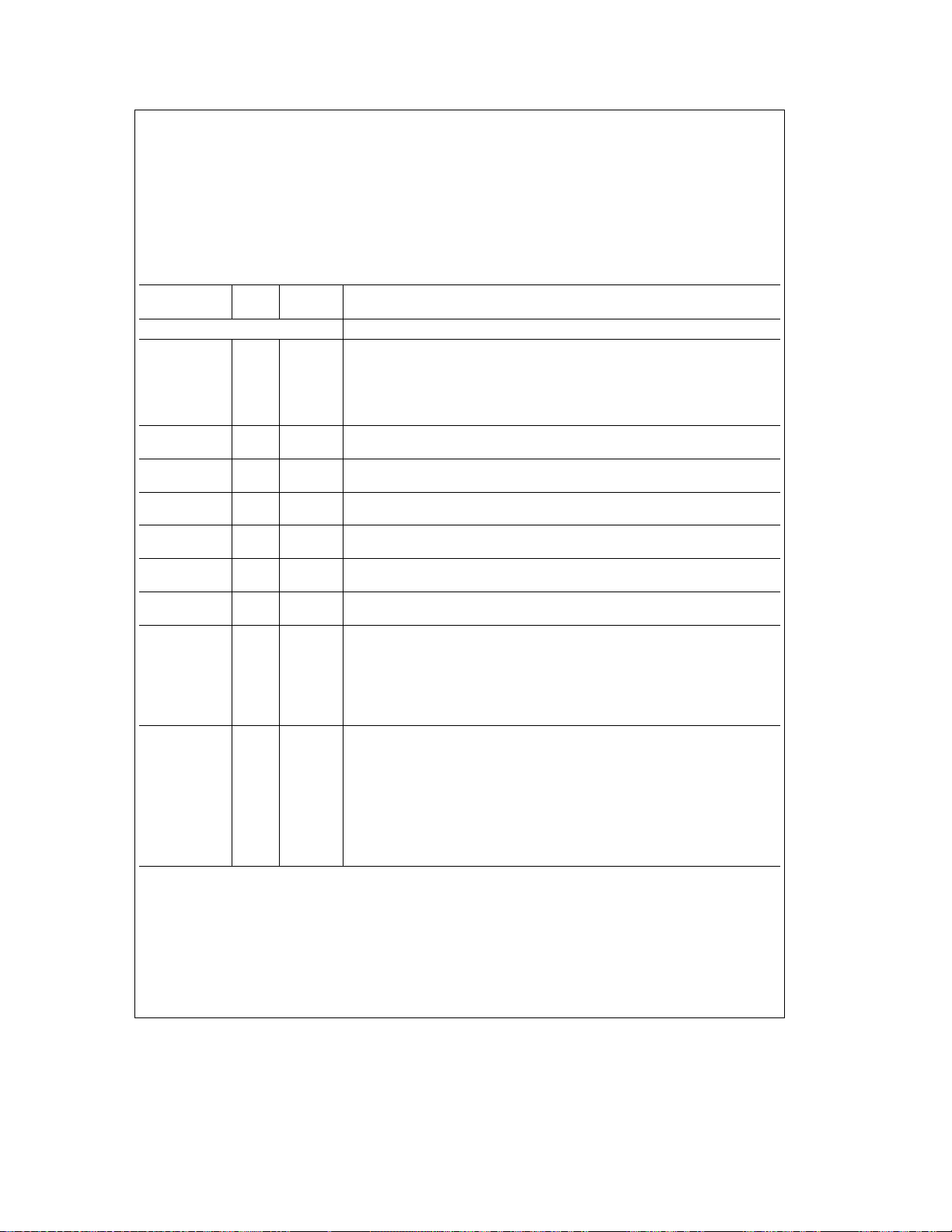
5.0 Bus Interface (Continued)
e
TRI
5.2 PIN DESCRIPTION
e
I
input,
Oeoutput, and
e
TRI-STATE Inputs are TTL compatible
Z
ECLeECL-like drivers for interfacing to the AUI interface.
TPeTotem pole like drivers. These drivers are driven ei-
ther high or low and are always driven. Drive levels
are CMOS compatible.
TABLE 5-1. Pin Description
Symbol
Driver
Type
Direction Description
NETWORK INTERFACE PINS
EXT I External ENDEC Select: Tying this pin to VCC(EXTe1) disables the internal ENDEC
and allows an external ENDEC to be used. Tying this pin to ground (EXT
the internal ENDEC. This pin must be tied either to V
pin definitions for CRSo/CRSi, COLo/COLi, RXDo/RXDi, RXCo/RXCi, and TXCo/TXCi.
When EXT
e
0 the first pin definition is used and when EXTe1 the second pin definition
is used.
a
CD
I Collisiona: The positive differential collision input from the transceiver. This pin should
be unconnected when an external ENDEC is selected (EXTe1).
b
CD
I Collisionb: The negative differential collision input from the transceiver. This pin
should be unconnected when an external ENDEC is selected (EXT
a
RX
I Receivea: The positive differential receive data input from the transceiver. This pin
should be unconnected when an external ENDEC is selected (EXT
b
RX
I Receiveb: The negative differential receive data input from the transceiver. This pin
should be unconnected when an external ENDEC is selected (EXT
a
TX
ECL O Transmita: The positive differential transmit output to the transceiver. This pin should
be unconnected when an external ENDEC is selected (EXT
b
TX
ECL O Transmitb: The negative differential transmit output to the transceiver. This pin should
be unconnected when an external ENDEC is selected (EXT
CRSo TP O Carrier Sense Output (CRSo) from the internal ENDEC (EXTe0): When EXTe0 the
CRSi I
CRSo signal is internally connected between the ENDEC and MAC units. It is asserted
on the first valid high-to-low transition in the receive data (RX
active 1.5 bit times after the last bit of data. Although this signal is used internally by the
SONIC-16 it is also provided as an output to the user.
Carrier Sense Input (CRSi) from an external ENDEC (EXT
activated high when the external ENDEC detects valid data at its receive inputs.
COLo TP O Collision Output (COLo) from the internal ENDEC (EXTe0): When EXTe0 the
COLi I
COLo signal is internally connected between the ENDEC and MAC units. This signal
generates an active high signal when the 10 MHz collision signal from the transceiver is
detected. Although this signal is used internally by the SONIC-16 it is also provided as
an output to the user.
Collision Detect Input (COLi) from an external ENDEC (EXT
activated from an external ENDEC when a collision is detected. This pin is monitored
during transmissions from the beginning of the Start Of Frame Delimiter (SFD) to the
end of the packet. At the end of transmission, this signal is monitored by the SONIC-16
for CD heartbeat.
TRI-STATE drivers. These pins are driven high, low
or TRI-STATE. Drive levels are CMOS compatible.
These pins may also be inputs (depending on the
pin).
e
OC
Open Collector type drivers. These drivers are
TRI-STATE when inactive and are driven low when
active. These pins may also be inputs (depending
on the pin).
or ground. Note the alternate
CC
e
e
e
e
1).
e
1).
a/b
). This signal remains
e
1): The CRSi signal is
e
1): The COLi signal is
e
1).
1)
1)
0) enables
45
Page 46

5.0 Bus Interface (Continued)
TABLE 5-1. Pin Description (Continued)
Symbol
NETWORK INTERFACE PINS (Continued)
RXDo TP O This pin will be TRI-STATE until the DCR has been written to. (See section 4.3.2,
RXDi I
EXUSR0 TRI O, Z
RXCo TP O This pin will be TRI-STATE until the DCR has been written to. (See section 4.3.2,
RXCi I
EXUSR1 TRI O, Z
TXD TP O This pin will be TRI-STATE until the DCR has been written to. (See section 4.3.2,
EXUSR3 TRI O, Z
TXE TP O Transmit Enable: This pin is driven high when the SONIC-16 begins transmission and
TXCo TRI O, Z This pin will be TRI-STATE until the DCR has been written to. (See section 4.3.2,
TXCi I
STERM
Driver
Type
Direction Description
EXBUS, for more information.)
Receive Data Output (RXDo) from the internal ENDEC (EXT
When EXT
MAC units. This signal must be sampled on the rising edge of the receive clock output
(RXCo). Although this signal is used internally by the SONIC-16 it is also provided as an
output to the user.
Receive Data Input (RXDi) from an external ENDEC (EXT
decoded from the external ENDEC. This data is clocked in on the rising edge of RXCi.
Extended User Output (EXUSR0): When EXBUS has been set (see section 4.3.2), this
pin becomes a programmable output. It will remain TRI-STATE until the SONIC-16
becomes a bus master, at which time it will be driven according to the value
programmed in the DCR2 (Section 4.3.7).
EXBUS, for more information.)
Receive Clock Output (RXCo) from the internal ENDEC (EXTe0): When EXTe0
the RXCo signal is internally connected between the ENDEC and MAC units. This signal
is the separated receive clock from the Manchester data stream. It remains active 5-bit
times after the deassertion of CRSo. Although this signal is used internally by the
SONIC-16 it is also provided as an output to the user.
Receive Clock Input (RXCi) from an external ENDEC (EXT
received clock from the Manchester data stream. This signal is generated from an
external ENDEC.
Extended User Output (EXUSR1): When EXBUS has been set (see section 4.3.2), this
pin becomes a programmable output. It will remain TRI-STATE until the SONIC-16
becomes a bus master, at which time it will be driven according to the value
programmed in the DCR2 (Section 4.3.7).
EXBUS, for more information.)
Transmit Data (TXD): The serial NRZ data from the MAC unit which is to be decoded
by an external ENDEC. Data is valid on the rising edge of TXC. Although this signal is
used internally by the SONIC-16 it is also provided as an output to the user.
Extended User Output (EXUSR3): When EXBUS has been set (see section 4.3.2), this
pin becomes a programmable output. It will remain TRI-STATE until the SONIC-16
becomes a bus master, at which time it will be driven according to the value
programmed in the DCR2 (Section 4.3.7).
remains active until the last byte is transmitted. Although this signal is used internally by
the SONIC-16 it is also provided as an output to the user.
EXBUS, for more information.)
Transmit Clock Output (TXCo) from the internal ENDEC (EXT
I
clock transmit clock output is derived from the 20 MHz oscillator. When EXT
TXCOUT signal is internally connected between the ENDEC and MAC units. Although
this signal is used internally by the SONIC-16 it is also provided as an output to the user.
Transmit Clock Input (TXCi) (EXT
used for shifting data out of the MAC unit serializer. This clock is nominally 10 MHz.
Synchronous Termination (STERM): When the SONIC-16 is a bus master, it samples
this pin before terminating its memory cycle. This pin is sampled synchronously and may
only be used in asynchronous bus mode when BMODE
details.
e
0 the RXDOUT signal is internally connected between the ENDEC and
e
1): This input clock from an external ENDEC is
e
0): NRZ data output.
e
1): The NRZ data
e
1): The separated
e
0): This 10 MHz
e
0 the
e
1. See section 5.4.5 for more
46
Page 47
5.0 Bus Interface (Continued)
TABLE 5-1. Pin Description (Continued)
Symbol
NETWORK INTERFACE PINS (Continued)
LBK TP O This pin will be TRI-STATE until the DCR has been written to. (See Section 4.3.2,
EXUSR2 TRI O, Z EXBUS, for more information.)
PCOMP TRI O, Z Packet Compression: This pin is used with the Management Bus of the DP83950,
SEL I Mode Select (EXTe0): This pin is used to determine the voltage relationship between
PREJ I, O Packet Reject: This signal is used to reject received packets. When asserted low for at
X1 TP I Crystal or External Oscillator Input: This signal is used to provide clocking signals for
X2 I, O Crystal Feedback Output: This signal is used to provide clocking signals for the
BUS INTERFACE PINS
BMODE I Bus Mode: This input enables the SONIC-16 to be compatible with standard
D31–D0 TRI I, O, Z Data Bus: These bidirectional lines are used to transfer data on the system bus. When
Driver
Type
Direction Description
Loopback (LBK): When ENDEC loopback is programmed, this pin is asserted high.
Although this signal is used internally by the SONIC-16 it is also provided as an output to
the user.
Extended User Output (EXUSR2): When EXBUS has been set (see Section 4.3.2), this
pin becomes a programmable output. It will remain TRI-STATE until the SONIC-16
becomes a bus master, at which time it will be driven according to the value
programmed in the DCR2 (Section 4.3.7).
Repeater Interface Controller (RIC). The SONIC-16 can be programmed to assert
PCOMP
whenever there is a CAM match, or when there is not a match. The RIC uses
this signal to compress (shorten) a received packet for management purposes and to
reduce memory usage. (See the DP83950 datasheet for more details on the RIC
Management Bus.) The operation of this pin is controlled by bits 1 and 2 in the DCR2
register. PCOMP will remain TRI-STATE until these bits are written to.
a
TX
and TXbduring idle at the primary of the isolation transformer on the network
interface. When tied to V
to ground, the voltage at TX
side of the isolation transformer (
least two receive clocks (RXC), the SONIC-16 will reject the incoming packet. This pin
can be asserted up to the 2nd to the last bit of reception to reject a packet.
the internal ENDEC. A crystal can be connected to this pin along with X2, or an
oscillator module may be used. Typically the output of an oscillator module is connected
to this pin. See Section 6.1.3 for more information about using oscillators or crystals.
internal ENDEC. A crystal may be connected to this pin along with X1, or an oscillator
module may be used. See Section 6.1.3 for more information about using oscillator
modules or crystals.
microprocessor buses. The level of this pin affects byte ordering (little or big endian) and
controls the operation of the bus interface control signals. A high level (tied to V
selects Motorola mode (big endian) and a low level (tied to ground) selects National/
Intel mode (little endian). Note the alternate pin definitions for AS
INT
/INT, BR/HOLD, BG/HLDA, SRW/SWR, DSACK0/RDYi, and DSACK1/RDYo.
When BMODE
definition is used. See Sections 5.4.1, 5.4.4, and 5.4.5.
the SONIC-16 is a bus master, 16-bit data is transferred on D15–D0 and 32-bit data is
transferred on D31–D0. When the SONIC-16 is accessed as a slave, register data is
driven onto lines D15–D0.
e
,TXaand TXbare at equal voltages during idle. When tied
CC
a
is positive with respect to TXbduring idle on the primary
Figure 6-2
1 the first pin definition is used and when BMODEe0 the second pin
).
CC
/ADS, MRW/MWR,
)
47
Page 48
5.0 Bus Interface (Continued)
TABLE 5-1. Pin Description (Continued)
Symbol
BUS INTERFACE PINS (Continued)
A31–A1 TRI O, Z Address Bus: These signals are used by the SONIC-16 to drive the DMA address after
RA5–RA0 I Register Address Bus: These signals are used to access SONIC-16’s internal
AS TRI I, O, Z Address Strobe (AS): When BMODEe1, the falling edge indicates valid status and
ADS
MRW TRI O, Z When the SONIC-16 has acquired the bus, this signal indicates the direction of data.
MWR
INT OC O, Z Indicates that an interrupt (if enabled) is pending from one of the sources indicated by
INT TP O
RESET I Reset: This signal is used to hardware reset the SONIC-16. When asserted low, the
S2–S0 TP O Bus Status: These three signals provide a continuous status of the current SONIC-16
BSCK I Bus Clock: This clock provides the timing for the SONIC-16 DMA engine.
BR OC O, Z Bus Request (BR): When BMODEe1, the SONIC-16 asserts this pin low when it
HOLD TP O
BG I Bus Grant (BG): When BMODEe1 this signal is a bus grant. The system asserts this
HLDA I
BGACK TRI I, O, Z Bus Grant Acknowledge: When BMODEe1, the SONIC-16 asserts this pin low when
Driver
Direction Description
Type
the SONIC-16 has acquired the bus. Since the SONIC-16 aligns data to word
boundaries, only 23 address lines are needed.
registers. When the SONIC-16 is accessed, the CPU drives these lines to select the
desired SONIC-16 register.
TRI O, Z
TRI O, Z Memory Read/Write Strobe (MRW): When BMODEe1, this signal is high during a
address. The rising edge indicates the termination of the memory cycle.
Address Strobe (ADS
address.
read cycle and low during a write cycle.
Memory Read/Write Strobe (MWR
read cycle and high during a write cycle.
the Interrupt Status register. Interrupts that are disabled in the Interrupt Mask register
will not activate this signal.
Interrupt (INT
Interrupt (INT): This signal is active high when BMODE
SONIC-16 transitions into the reset state after 10 transmit clocks or 10 bus clocks if the
bus clock period is greater than the transmit clock period.
bus operations. See Section 5.4.3 for status definitions.
attempts to gain access to the bus. When inactive this signal is at TRI-STATE.
Hold Request (HOLD): When BMODEe0, the SONIC-16 drives this pin high when it
intends to use the bus and is driven low when inactive.
pin low to indicate potential mastership of the bus.
Hold Acknowledge (HLDA): When BMODE
SONIC-16 that it has attained the bus. When the system asserts this pin high, the
SONIC-16 has gained ownership of the bus.
it has determined that it can gain ownership of the bus. The SONIC-16 checks the
following signal before driving BGACK
arbitration process. 2) AS
bus. 3) DSACK0
is off the bus. 4) BGACK
This pin is only used when BMODE
): When BMODEe0, the rising edge indicates valid status and
): When BMODEe0, the signal is low during a
): This signal is active low when BMODEe1.
e
is deasserted, indicating that the CPU has finished using the
and DSACK1 are deasserted, indicating that the previous slave device
is deasserted, indicating that the previous master is off the bus.
.1)BGhas been received through the bus
e
1.
e
0.
0 this signal is used to inform the
48
Page 49

5.0 Bus Interface (Continued)
TABLE 5-1. Pin Description (Continued)
Symbol
BUS INTERFACE PINS (Continued)
CS I Chip Select: The system asserts this pin low to access the SONIC-16’s registers. The
SAS I Slave Address Strobe: The system asserts this pin to latch the register address on
SDS I Slave Data Strobe: The system asserts this pin to indicate valid data is on the bus
SRW I The system asserts this pin to indicate whether it will read from or write to the SONICSWR
DS TRI O, Z Data Strobe: When the SONIC-16 is bus master, it drives this pin low during a read
DSACK0 TRI I, O, Z Data and Size Acknowledge 0 and 1 (DSACK0,1 BMODEe1): These pins are the
RDYi I
DSACK1
RDYo
BRT I Bus Retry: When the SONIC-16 is bus master, the system asserts this signal to rectify a
ECS TRI O, Z Early Cycle Start: This output gives the system earliest indication that a memory
Driver
Direction Description
Type
TRI I, O, Z
TRI O, Z
registers are selected by placing an address on lines RA5–RA0.
Note: Both CS
successively asserted, there must be at least two bus clocks between the deasserting
edge of the first signal and the asserting edge of the second signal.
lines RA0–RA5. When BMODE
When BMODEe0 the address is latched on the rising edge of SAS.
during a register write operation or when data may be driven onto the bus during a
register read operation.
16’s registers.
I
Slave Read/Write (SRW
read and low during a write.
Slave Read/Write Strobe (SWR
a read and high during a write.
cycle to indicate that the slave device may drive data onto the bus; in a write cycle, this
pin indicates that the SONIC-16 has placed valid data onto the bus.
output slave acknowledge to the system when the SONIC-16 registers have been
accessed and the input slave acknowledgement when the SONIC-16 is busmaster.
When a register has been accessed, the SONIC-16 drives the DSACK0,1
terminate the slave cycle. (Note that the SONIC-16 responds as a 32-bit peripheral, but
drives data only on lines D0–D15). When the SONIC-16 is bus master, it samples these
pins before terminating its memory cycle. These pins are sampled synchronously or
asynchronously depending on the state of the SBUS bit in the Data Configuration
register. See Section 5.4.5 for details. Note that the SONIC-16 does not allow dynamic
bus sizing.
Ready Input (RDYi, BMODEe0): When the SONIC-16 is a bus master, the system
asserts this signal high to insert wait-states and low to terminate the memory cycle. This
signal is sampled synchronously or asynchronously depending on the state of the SBUS
bit. See Sections 5.4.5 and 4.3.2 for details.
Ready Output (RDYo
asserts this signal to terminate the slave cycle.
potentially correctable bus error. This pin has 2 modes. Mode 1 (the LBR in the Data
Configuration register is set to 0): Assertion of this pin forces the SONIC-16 to terminate
the current bus cycle and will repeat the same cycle after BRT
Mode 2 (the LBR bit in the Data Configuration register is set to 1): Assertion of this
signal forces the SONIC-16 to retry the bus operation as in Mode 1. However, the
SONIC-16 will not continue DMA operations until the BR bit in the ISR is reset.
operation is occurring. This signal is driven low at the rising edge of T1 and high at the
falling edge of T1.
and MREQ must not be asserted concurrently. If these signals are
e
1, the address is latched on the falling edge of SAS.
): When BMODEe1, this signal is asserted high during a
): when BMODEe0, this signal is asserted low during
, BMODEe0): When a register is accessed, the SONIC-16
has been deasserted.
pins low to
49
Page 50

5.0 Bus Interface (Continued)
TABLE 5-1. Pin Description (Continued)
Symbol
SHARED-MEMORY ACCESS PINS
MREQ I Memory Request: The system asserts this signal low when it attempts to access the
SMACK TP O Slave and Memory Acknowledge: SONIC-16 asserts this dual function pin low in
USER DEFINABLE PINS
USR0,1 TRI I, O, Z User Define 0,1: These signals are inputs when SONIC-16 is hardware reset and are
POWER AND GROUND PINS
VCC1–5 Power: Thea5V power supply for the digital portions of the SONIC-16.
TXVCC Power: These pins are thea5V power supply for the SONIC-16 ENDEC unit. These
RXVCC
PLLVCC
VCCL
GND1–6 Ground: The ground reference for the digital portions of the SONIC-16.
TXGND Ground: These pins are the ground references for the SONIC-16 ENDEC unit. These
ANGND
GNDL
Driver
Type
Direction Description
shared-buffer RAM. The on-chip arbiter resolves accesses between the system and the
SONIC-16.
Note: Both CS
successively asserted, there must be at least two bus clocks between the deasserting
edge of the first signal and the asserting edge of the second signal.
response to either a Chip Select (CS) or a Memory Request (MREQ) when the SONIC16’s registers or it’s buffer memory is available for accessing. This pin can be used for
enabling bus drivers for dual-bus systems.
outputs when SONIC-16 is a bus master (HLDA or BGACK
low, these signals input directly into bits 8 and 9 of the Data Configuration register
(DCR) respectively. The levels on these pins are latched on the rising edge of RST
During busmaster operations (HLDA or BGACK
levels are programmable through bits 11 and 12 of the DCR respectively. The USR0,1
pins should be pulled up to V
recommended.
pins must be tied to V
pins must be tied to ground even if the internal ENDEC is not used.
and MREQ must not be asserted concurrently. If these signals are
is active), these pins are outputs whose
or pulled down to ground. A 4.7 kX pull-up resistor is
CC
even if the internal ENDEC is not used.
CC
). When hard reset (RST)is
.
50
Page 51

5.0 Bus Interface (Continued)
5.3 SYSTEM CONFIGURATION
Any device that meets the SONIC-16 interface protocol and
electrical requirements (timing, threshold, and loading) can
be interfaced to SONIC-16. Since two bus protocols are provided, via the BMODE pin, the SONIC-16 can interface directly to most microprocessors.
interface to the National/Intel style bus (BMODE
Figure 5-4
bus (BMODE
The BMODE pin also controls byte ordering. When
BMODE
BMODE
shows a typical interface to the Motorola style
e
1).
e
1 big endian byte ordering is selected and when
e
0 little endian byte ordering is selected.
Figure 5-3
shows a typical
e
0) and
5.4 BUS OPERATIONS
There are two types of system bus operations: 1) SONIC-16
as a slave, and 2) SONIC-16 as a bus master. When
SONIC-16 is a slave (e.g., a CPU accessing SONIC-16 registers) all transfers are non-DMA. When SONIC-16 is a bus
master (e.g., SONIC-16 accessing receive or transmit buffer/descriptor areas) all transfers are block transfers using
SONIC-16’s on-chip DMA. This section describes the
SONIC-16 bus operations. Pay special attention to all sections labeled as ‘‘Note’’. These conditions must be met for
proper bus operation.
FIGURE 5-3. SONIC-16 to NS32532 Interface Example
51
TL/F/11722– 25
Page 52
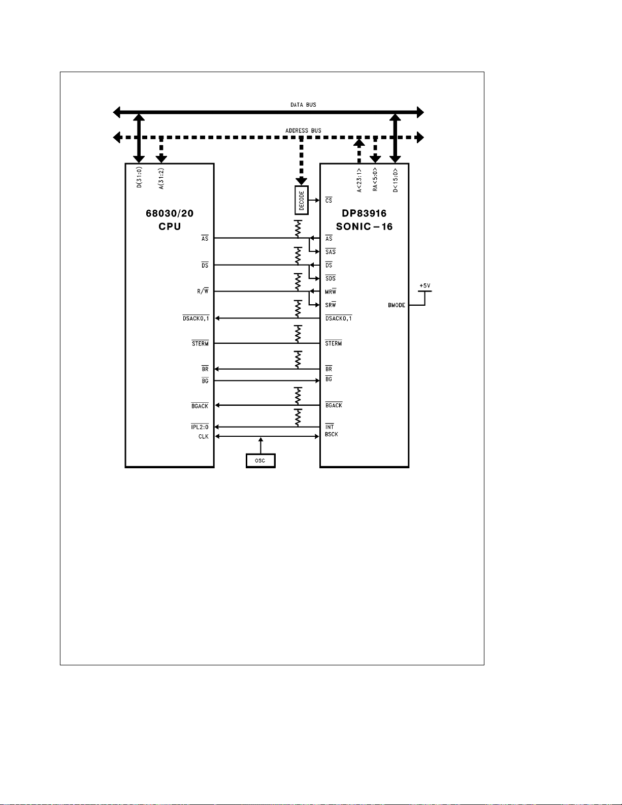
5.0 Bus Interface (Continued)
FIGURE 5-4. SONIC-16 to Motorola 68030/20 Interface Example
52
TL/F/11722– 26
Page 53

5.0 Bus Interface (Continued)
5.4.1 Acquiring The Bus
The SONIC-16 requests the bus when 1) its FIFO threshold
has been reached or 2) when the descriptor areas in memory (i.e., RRA, RDA, CDA, and TDA) are accessed. Note that
when the SONIC-16 moves from one area in memory to
another (e.g., RBA to RDA), it always deasserts its bus request and then requests the bus again when accessing the
next area in memory.
The SONIC-16 provides two methods to acquire the bus for
compatibility with National/Intel or Motorola type microprocessors. These two methods are selected by setting the
proper level on the BMODE pin.
Figures 5-5
and Motorola (BMODE
tions of each mode follows. For both modes, when the
SONIC-16 relinquishes the bus, there is an extra holding
state (Th) for one bus cycle after the last DMA cycle (T2).
This assures that the SONIC-16 does not contend with another bus master after it has released the bus.
BMODE
The National/Intel processors require a 2-way handshake
using a HOLD REQUEST/HOLD ACKNOWLEDGE protocol
(
Figure 5-5
it issues a HOLD REQUEST (HOLD) to the microprocessor.
The microprocessor, responds with a HOLD ACKNOWLEDGE (HLDA) to the SONIC-16. The SONIC-16 then begins
its memory transfers on the bus. As long as the CPU maintains HLDA active, the SONIC-16 continues until it has finished its memory block transfer. The CPU, however, can
preempt the SONIC-16 from finishing the block transfer by
deasserting HLDA before the SONIC-16 deasserts HOLD.
This allows a higher priority device to preempt the SONIC16 from continuing to use the bus. The SONIC-16 will request the bus again later to complete any operation that it
was doing at the time of preemption.
and
5-6
show the National/Intel (BMODEe0)
e
1) bus request timing. Descrip-
e
0
). When the SONIC-16 needs to access the bus,
As shown in
either the falling or rising edge of the bus clock (BSCK). The
default is for HOLD to be asserted on the falling edge. Setting the PH bit in the DCR2 (see Section 4.3.7) causes
HOLD to be asserted (/2 bus clock later on the rising edge
(shown by the dotted line). Before HOLD is asserted, the
SONIC-16 checks the HLDA line. If HLDA is asserted,
HOLD will not be asserted until after HLDA has been deasserted first.
BMODE
The Motorola protocol requires a 3-way handshake using a
BUS REQUEST, BUS GRANT, and BUS GRANT ACKNOWLEDGE handshake (
protocol, the SONIC-16 requests the bus by lowering BUS
REQUEST (BR
GRANT (BG
that all devices have relinquished control of the bus before
using the bus. The following signals must be deasserted
before the SONIC-16 acquires the bus:
BGACK
AS
DSACK0,1
STERM (Asynchronous Mode Only)
Deasserting BGACK indicates that the previous master has
released the bus. Deasserting AS
ous master has completed its cycle and deasserting
DSACK0,1
has terminated its connection to the previous master. The
SONIC-16 maintains its mastership of the bus until it deasserts BGACK
Figure 5-5,
e
1
). Upon receiving BG, the SONIC-16 assures
and STERM indicates that the previous slave
. It can not be preempted from the bus.
the SONIC-16 will assert HOLD to
Figure 5-6
). The CPU responds by issuing BUS
). When using this
indicates that the previ-
FIGURE 5-5. Bus Request Timing, BMODEe0
53
TL/F/11722– 27
Page 54

5.0 Bus Interface (Continued)
FIGURE 5-6. Bus Request Timing, BMODEe1
5.4.2 Block Transfers
The SONIC-16 performs block operations during all bus actions, thereby providing efficient transfers to memory. The
block cycle consists of three parts. The first part is the bus
acquisition phase, as discussed above, in which the SONIC16 gains access to the bus. Once it has access of the bus,
the SONIC-16 enters the second phase by transferring data
to/from its internal FIFOs or registers from/to memory. The
SONIC-16 transfers data from its FIFOs in either EXACT
BLOCK mode or EMPTY/FILL.
EXACT BLOCK mode: In this mode the number of words
(or long words) transferred during a block transfer is determined by either the Transmit or Receive FIFO thresholds
programmed in the Data Configuration Register.
EMPTY/FILL mode: In this mode the DMA completely fills
the Transmit FIFO during transmission, or completely empties the Receive FIFO during reception. This allows for
greater bus latency.
When the SONIC-16 accesses the Descriptor Areas (i.e.,
RRA, RDA, CDA, and TDA), it transfers data between its
registers and memory. All fields which need to be used are
accessed in one block operation. Thus, the SONIC-16 performs 4 accesses in the RRA (see Section 3.4.4.2), 7 accesses in the RDA (see Section 3.4.6.1), 2, 3, or 6 accesses
in the TDA (see Section 3.5.4) and 4 accesses in the CDA.
5.4.3 Bus Status
The SONIC-16 presents three bits of status information on
pins S2–S0 which indicate the type of bus operation the
SONIC-16 is currently performing (Table 5-2). Bus status is
valid when at the falling edge of AS
ADS
.
or the rising edge of
TL/F/11722– 28
TABLE 5-2. Bus Status
S2 S1 S0 Status
1 1 1 The bus is idle. The SONIC-16 is not
performing any transfers on the bus.
1 0 1 The Transmit Descriptor Area (TDA) is
currently being accessed.
0 0 1 The Transmit Buffer Area (TBA) is
currently being read.
0 1 1 The Receive Buffer Area (RBA) is
currently being written to. Only data is
being written, though, not a Source or
Destination address.
0 1 0 The Receive Buffer Area (RBA) is
currently being written to. Only the
Source or Destination address is being
written, though.
1 1 0 The Receive Resource Area (RRA) is
currently being read.
1 0 0 The Receive Descriptor Area (RDA) is
currently being accessed.
0 0 0 The CAM Descriptor Area (CDA) is
currently being accessed.
54
Page 55
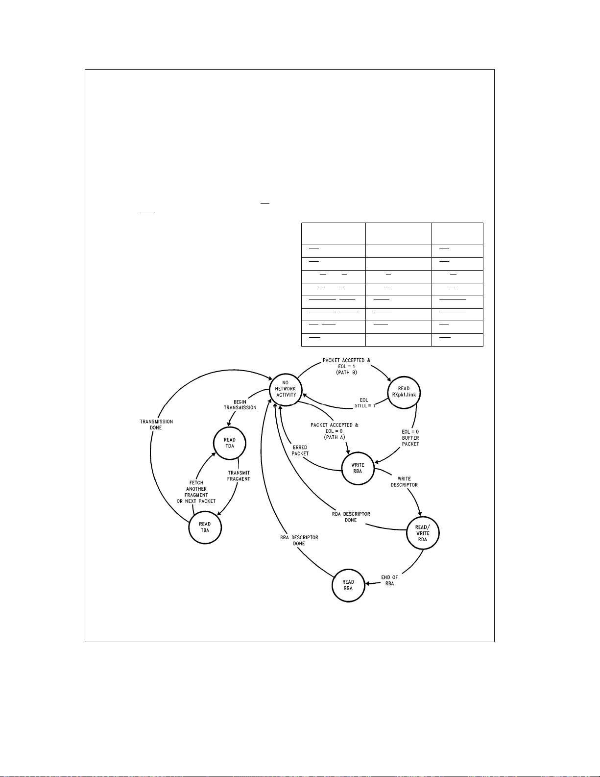
5.0 Bus Interface (Continued)
5.4.3.1 Bus Status Transitions
When the SONIC-16 acquires the bus, it only transfers data
to/from a single area in memory (i.e., TDA, TBA, RDA, RBA,
RRA, or CDA). Thus, the bus status pins remain stable for
the duration of the block transfer cycle with the following
three exceptions: 1) If the SONIC-16 is accessed during a
block transfer, S2 – S0 indicates bus idle during the register
access, then returns to the previous status. 2) If the SONIC16 finishes writing the Source Address during a block transfer S2 –S0 changes from[0,1,0]to[0,1,1]. 3) During an
RDA access between the RXpkt.seqÐno and RXpkt.link access, and between the RXpkt.link and RXpkt.inÐuse access, S2 – S0 will respectively indicate idle[1,1,1]for2or1
bus clocks. Status will be valid on the falling edge of AS
rising edge of ADS
Figure 5-7
memory during the process of transmission and reception.
During transmission, the SONIC-16 reads the descriptor information from the TDA and then transmits data of the
packet from the TBA. The SONIC-16 moves back and forth
between the TDA and TBA until all fragments and packets
are transmitted. During reception, the SONIC-16 takes one
of two paths. In the first case (path A), when the SONIC-16
detects EOL
accepted packet into the RBA, and then writes the descriptor information to the RDA. If the RBA becomes depleted
(i.e., RBWC0,1
resource descriptor. In the second case (path B), when the
SONIC-16 detects EOL
.
illustrates the SONIC-16’s transitions through
e
0 from the previous reception, it buffers the
k
EOBC), it moves to the RRA to read a
e
1 from the previous reception, it
rereads the RXpkt.link field to determine if the system has
reset the EOL bit since the last reception. If it has, the SONIC-16 buffers the packet as in the first case. Otherwise, it
rejects the packet and returns to idle.
5.4.4 Bus Mode Compatibility
For compatibility with different microprocessor and bus architectures, the SONIC-16 operates in one of two modes
(set by the BMODE pin) called the National/Intel or little
endian mode (BMODE tied low) and the Motorola or big
endian mode (BMODE tied high). The definitions for several
pins change depending on the mode the SONIC-16 is in.
Table 5-3 shows these changes. These modes affect both
master and slave bus operations with the SONIC-16.
or
TABLE 5-3. Bus Mode Compatibility
e
Pin Name
BMODE
(National/Intel) (Motorola)
0 BMODEe1
BR/HOLD HOLD BR
BG/HLDA HLDA BG
MRW/MWR MWR MRW
SRW/SWR SWR SRW
DSACK0/RDYi RDYi DSACK0
DSACK1/RDYo RDYo DSACK1
AS/ADS ADS AS
INT/INT INT INT
FIGURE 5-7. Bus Status Transitions
55
TL/F/11722– 29
Page 56

5.0 Bus Interface (Continued)
5.4.5 Master Mode Bus Cycles
In order to add additional compatibility with different bus
architectures, there are two other modes that affect the operation of the bus. These modes are called the synchronous
and asynchronous modes and are programmed by setting
or resetting the SBUS bit in the Data Configuration Register
(DCR). The synchronous and asynchronous modes do not
have an effect on slave accesses to the SONIC-16 but they
do affect the master mode operation. Within the particular
bus/processor mode, synchronous and asynchronous
modes are very similar. This section discusses all four
modes of operation of the SONIC-16 (National/Intel vs. Motorola, synchronous vs. asynchronous) when it is a bus master.
In this section, the rising edge of T1 and T2 means the
beginning of these states, and the falling edge of T1 and T2
means the middle of these states.
5.4.5.1 Adding Wait States
To accommodate different memory speeds, the SONIC-16
provides two methods for adding wait states for its bus operations. Both of these methods can be used singly or in
conjunction with each other. A memory cycle is extended by
adding additional T2 states. The first method inserts waitstates by withholding the assertion of DSACK0,1
RDYi
. The other method allows software to program waitstates. Programming the WC0, WC1 bits in the Data Configuration Register allows 1 to 3 wait-states to be added on
each memory cycle. These wait states are inserted between
the T1 and T2 bus states and are called T2(wait) bus states.
The SONIC-16 will not look at the DSACK0,1,
RDYi
lines until the programmed wait states have passed.
Hence, in order to complete a bus operation that includes
programmed wait states, the DSACK0,1,
lines must be asserted at their proper times at the end of the
cycle during the last T2, not during a programmed wait
state. The only exception to this is asynchronous mode
where DSACK0,1
programmed wait state, T2 (wait). See the timing for these
signals in the timing diagrams for more specific information.
Programmed wait states do not affect Slave Mode bus cycles.
or RDYi would be asserted during the last
/STERM or
STERM or
STERM or RDYi
56
Page 57

5.0 Bus Interface (Continued)
e
5.4.5.2 Memory Cycle for BMODE
Mode
On the rising edge of T1, the SONIC-16 asserts ECS
indicate that the memory cycle is starting. The address
(A31–A1), bus status (S2–S0) and the direction strobe
(MRW
) are driven and do not change for the remainder of
the memory cycle. On the falling edge of T1, the SONIC-16
deasserts ECS
In synchronous mode, DSACK0,1 are sampled on the rising
edge of T2. T2 states will be repeated until DSACK0,1
and asserts AS.
1, Synchronous
are
sampled properly in a low state. DSACK0,1
setup and hold times with respect to the rising edge of bus
clock for proper operation.
to
During read cycles (
the falling edge of T2 and DS
of T1. For write cycles (
falling edge of T1. If there are wait states inserted, DS
asserted on the falling edge of T2. The SONIC-16 terminates the memory cycle by deasserting AS
falling edge of T2.
Figure 5-8
Figure 5-9
) data (D15 – D0) is latched at
is asserted at the falling edge
) data is driven on the
must meet the
is
and DS at the
FIGURE 5-8. Memory Read, BMODEe1, Synchronous (1 Wait-State)
FIGURE 5-9. Memory Write, BMODEe1, Synchronous (1 Wait-State)
57
TL/F/11722– 31
TL/F/11722– 33
Page 58

5.0 Bus Interface (Continued)
e
5.4.5.3 Memory Cycle for BMODE
Asynchronous Mode
On the rising edge of T1, the SONIC-16 asserts ECS
indicate that the memory cycle is starting. The address
(A23–A1), bus status (S2–S0) and the direction strobe
(MRW
) are driven and do not change for the remainder of
the memory cycle. On the falling edge of T1, the SONIC-16
deasserts ECS
and asserts AS.
In asynchronous mode, DSACK0,1 are asynchronously
sampled on the falling edge of both T1 and T2. DSACK0,1
1,
do not need to be synchronized to the bus clock because
the chip always resolves these signals to either a high or
low state. If a synchronous termination of the bus cycle is
to
required, however, STERM
may be used. STERM is sampled on the rising edge of T2 and must meet the setup and
hold times with respect to that edge for proper operation.
Meeting the setup time for DSACK0,1
tees that the SONIC-16 will terminate the memory cycle 1(/2
or STERM guaran-
FIGURE 5-10. Memory Read, BMODEe1, Asynchronous (1 Wait-State)
FIGURE 5-11. Memory Read, BMODEe1, Asynchronous (2 Wait-State)
58
TL/F/11722– 36
TL/F/11722– 37
Page 59

5.0 Bus Interface (Continued)
bus clocks after DSACK0,1
STERM
was sampled. T2 states will be repeated until
DSACK0,1
or STERM are sampled properly in a low state.
(see note below).
During read cycles (
latched at the falling edge of T2 and DS
falling edge of T1 . For write cycles (
data is driven on the falling edge of T1. If there are wait
were sampled, or 1 cycle after
Figure 5-10
and
5-11
Figures 5-12
), data (D15 –D0) is
is asserted at the
and
5-13
states inserted, DS
T2(wait). DS
is asserted on the falling edge of the first
is not asserted for zero wait state write cycles.
The SONIC-16 terminates the memory cycle by deasserting
AS
and DS at the falling edge of T2.
Note: If the setup time for DSACK0,1 is met during T1, or the setup time for
)
is met during the first T2, the full asynchronous bus cycle will
STERM
take only 2 bus clocks. This may be an unwanted situation. If so,
and STERM should be deasserted during T1 and the start
DSACK0,1
of T2 respectively.
FIGURE 5-12. Memory Write, BMODEe1, Asynchronous (1 Wait-State)
FIGURE 5-13. Memory Write, BMODEe1, Asynchronous (2 Wait-State)
59
TL/F/11722– 34
TL/F/11722– 35
Page 60
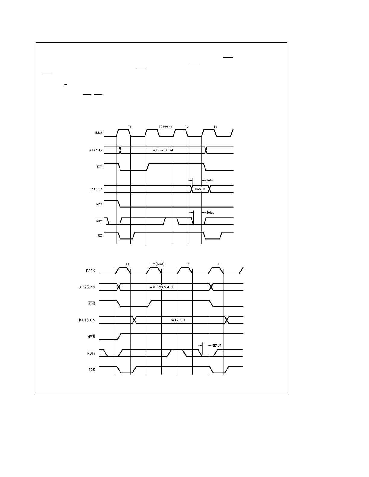
5.0 Bus Interface (Continued)
e
5.4.5.4 Memory Cycle for BMODE
Mode
On the rising edge of T1, the SONIC-16 asserts ADS
ECS
to indicate that the memory cycle is starting. The address (A23 – A1), bus status (S2– S0) and the direction
strobe (MWR
der of the memory cycle. On the falling edge of T1, the
SONIC-16 deasserts ECS
edge of T2.
In Synchronous mode, RDYi
at the end of T2 (the rising edge of the next T1 or Tx). T2
) are driven and do not change for the remain-
. ADS is deasserted on the rising
0, Synchronous
and
is sampled on the rising edge
states will be repeated until RDYi
low state. RDYi
respect to the rising edge of bus clock for proper operation.
During read cycles (
at the rising edge at the end of T2. For write cycles (
5-15
) data is driven on the falling edge of T1 and stays
driven until the end of the cycle.
must meet the setup and hold times with
Figures 5-14
is sampled properly in a
), data (D15 – D0) is latched
Figure
FIGURE 5-14. Memory Read, BMODEe0, Synchronous (1 Wait-State)
FIGURE 5-15. Memory Write, BMODEe0, Synchronous (1 Wait-State)
60
TL/F/11722– 38
TL/F/11722– 40
Page 61
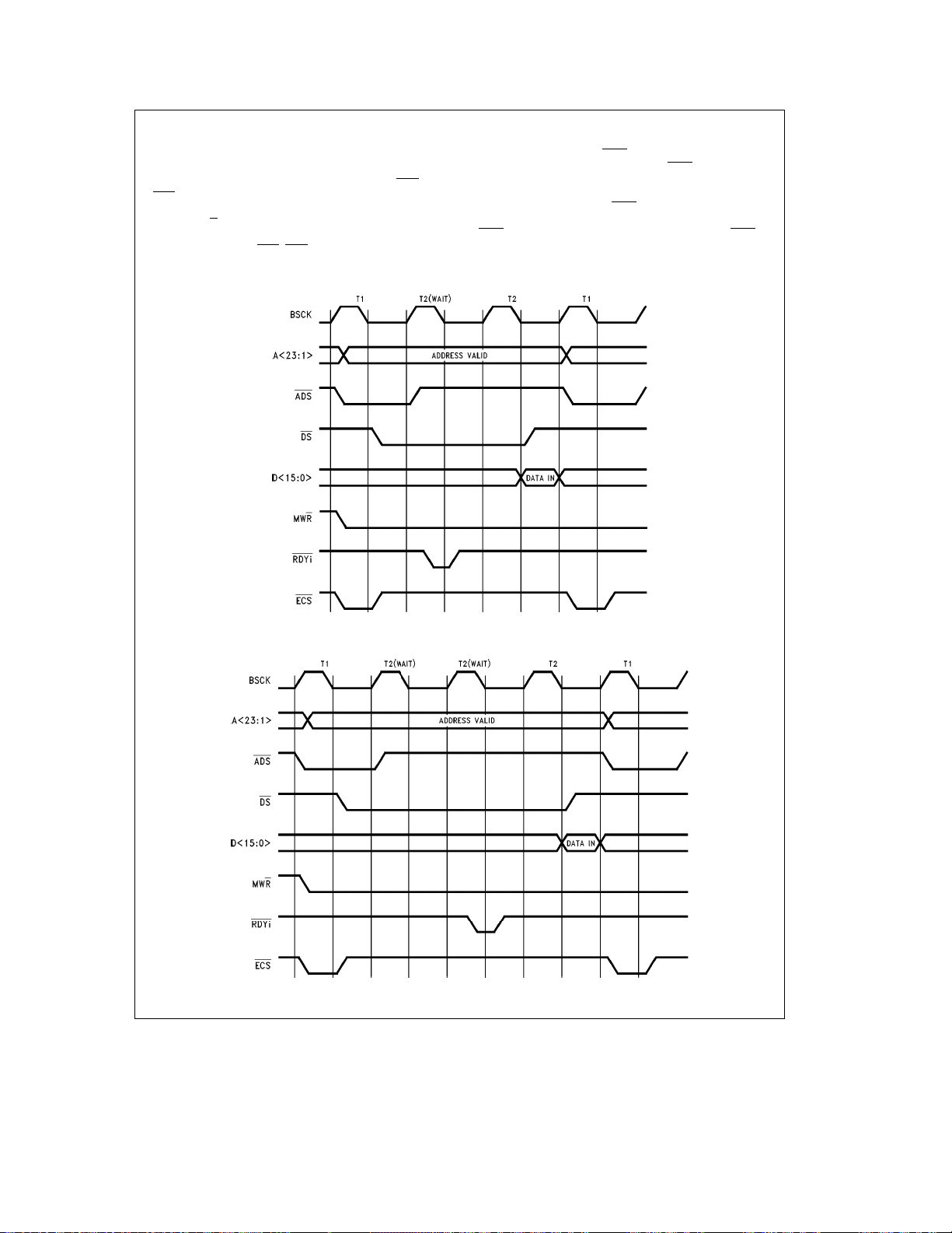
5.0 Bus Interface (Continued)
e
5.4.5.5 Memory Cycle for BMODE
Mode
On the rising edge of T1, the SONIC-16 asserts ADS
ECS
to indicate that the memory cycle is starting. The address (A23 – A1), bus status (S2– S0) and the direction
strobe (MWR
) are driven and do not change for the remainder of the memory cycle. On the falling edge of T1, the
SONIC-16 deasserts ECS
. ADS is deasserted on the rising
edge of T2.
0, Asynchronous
and
In Asynchronous mode, RDYi
on the falling edge of both T1 and T2. RDYi
is asynchronously sampled
does not need
to be synchronized to the bus clock because the chip always resolves these signals to either a high or low state.
Meeting the setup time for RDYi
guarantees that the SONIC-16 will terminate the memory cycle 1(/2 bus clocks after
RDYi
was sampled. T2 states will be repeated until RDYi is
sampled properly in a low state (see note following).
FIGURE 5-16. Memory Read, BMODEe0, Asynchronous (1 Wait-State)
FIGURE 5-17. Memory Read, BMODEe0, Asynchronous (2 Wait-State)
61
TL/F/11722– 42
TL/F/11722– 43
Page 62

5.0 Bus Interface (Continued)
During read cycles (
Figures 5-16
is latched at the falling edge of T2 and DS
falling edge of T1. For write cycles (
data is driven on the falling edge of T1. If there are wait
states inserted, DS
T2(wait). DS
is asserted on the falling edge of the first
is not asserted for zero wait state write cycles.
and
5-17
Figures 5-18
), data (D15–D0)
is asserted at the
and
5-19
The SONIC-16 terminates the memory cycle by deasserting
at the falling edge of T2.
DS
)
Note: If the setup time for RDYi is met during T1, the full asynchronous bus
cycle will take only 2 bus clocks. This may be an unwanted situation.
should be deasserted during T1.
If so, RDYi
FIGURE 5-18. Memory Write, BMODEe0, Asynchronous (1 Wait-State)
FIGURE 5-19. Memory Write, BMODEe0, Asynchronous (2 Wait-State)
62
TL/F/11722– 44
TL/F/11722– 45
Page 63

5.0 Bus Interface (Continued)
5.4.6 Bus Exceptions (Bus Retry)
The SONIC-16 provides the capability of handling errors
during the execution of the bus cycle (
The system asserts BRT (bus retry) to force the SONIC-16
to repeat the current memory cycle. When the SONIC-16
detects the assertion of BRT
cle at the end of T2 and gets off the bus by deasserting
BGACK
or HOLD. Then, if Latched Bus Retry mode is not
set (LBR in the Data Configuration Register, Section 4.3.2),
the SONIC-16 requests the bus again to retry the same
memory cycle. If Latched Bus Retry is set, though, the SONIC-16 will not retry until the BR bit in the ISR (see Section
4.3.6) has been reset and BRT
precedence of terminating a memory cycle over DSACK0,1
STERM
or RDYi.
BRT may be sampled synchronously or asynchronously by
setting the EXBUS bit in the DCR (see Section 4.3.2). If
synchronous Bus Retry is set, BRT
edge of T2. If asynchronous Bus Retry is set, BRT
synchronized from the falling edge of T1. The asynchronous
setup time does not need to be met, but doing so will guarantee that the bus exception will occur in the current bus
cycle instead of the next bus cycle. Asynchronous Bus Retry may only be used when the SONIC-16 is set to asynchronous mode.
Note 1: The deassertion edge of HOLD is dependent on the PH bit in the
DCR2 (see Section 4.3.7). Also, BGACK
bus clock before going TRI-STATE.
Note 2: If Latched Bus retry is set, BRT
hold time is not important). Otherwise, BRT
until after the Th state.
Note 3: If DSACK0,1
memory cycle, may be adversely affected.
, STERM or RDYi remain asserted after BRT, the next
5.4.7 Slave Mode Bus Cycle
The SONIC-16’s internal registers can be accessed by one
of two methods (BMODE
e
methods, the SONIC-16 is a slave on the bus. This section
describes the SONIC-16’s slave mode bus operations.
5.4.7.1 Slave Cycle for BMODE
The system accesses the SONIC-16 by driving SAS, SRW
and RAk5:0l. These signals will be sampled each bus cycle, but the SONIC-16 will not actually start a slave cycle
until CS
has also been asserted. CS should not be asserted
before SAS
is driven low as this will cause improper slave
Figure 5-20
).
, it completes the memory cy-
is deasserted. BRT has
is sampled on the rising
is double
is driven high for about (/2
need only satisfy its setup time (the
must remain asserted
1 or BMODEe0). In both
e
1
operation. Once SAS
has been driven low, between one
and two bus clocks after the assertion of CS
asserted to signify that the SONIC-16 has started the slave
cycle. Although CS
setup time (as shown in
tee that SMACK
is an asynchronous input, meeting its
Figures 5-21
and
, which is asserted off of a falling edge, will
be asserted 1 bus clock after the falling edge that CS
clocked in on. This is assuming that the SONIC-16 is not a
bus master when CS
master, then, when CS
was asserted. If the SONIC-16 is a bus
is asserted, the SONIC-16 will complete its current master bus cycle and get off the bus temporarily (see Section 5.4.8). In this case, SMACK
serted 5 bus clocks after the falling edge that CS
clocked in on. This is assuming that there were no wait
,
states in the current master mode access. Wait states will
increase the time for SMACK
to go low by the number of
wait states in the cycle.
If the slave access is a read cycle (
Figure 5-21
data will be driven off the same edge as SMACK
write cycle (
Figure 5-22
), then the data will be latched in
exactly 2 bus clocks after the assertion of SMACK
case, DSACK0,1
are driven low 2 bus clocks after SMACK
to terminate the slave cycle. For a read cycle, the assertion
of DSACK0,1
indicates valid register data and for a write
cycle, the assertion indicates that the SONIC-16 has
latched the data. The SONIC-16 deasserts DSACK0,1
SMACK
and the data if the cycle is a read cycle at the rising
edge of SAS
Note 1: Although the SONIC-16 responds as a 32-bit peripheral when it
Note 2: For multiple register accesses, CS
Note 3: If memory request (MREQ
Note 4: When CS
Note 5: The way in which SMACK
or CS depending on which is deasserted first.
drives DSACK0,1
used to delimit the slave cycle (this is the only case where CS
be asserted before SAS
due to SAS
that this means SMACK
time CS
asserted at least 2 bus clocks after CS
MREQ
bus clock.
the way in which SMACK
of SMACK
. This is not the same as the case for MREQ (see Section 5.4.8).
CS
The assertion of SMACK
fused.
low, it transfers data only on lines Dk15:0l.
going low since CS has already been asserted. Notice
is low (as is the case for MREQ, Section 5.4.8).
must not be asserted concurrently.
is deasserted, it must remain deasserted for at least one
is dependent upon both CS and SAS being low, not just
can be held low and SAS can be
). In this case, SMACK will be driven low
will not stay asserted low during the entire
) follows a chip select (CS), it must be
is deasserted. Both CS and
is asserted due to CS is not the same as
is asserted due to MREQ. The assertion
in these two cases should not be con-
, SMACK will be
5-22
) will guaran-
will be as-
), then the
.Ifitisa
. In either
is
was
,
may
FIGURE 5-20. Bus Exception (Bus Retry)
63
TL/F/11722– 46
Page 64

5.0 Bus Interface (Continued)
FIGURE 5-21. Register Read, BMODEe1
FIGURE 5-22. Register Write, BMODEe1
TL/F/11722– 47
TL/F/11722– 48
64
Page 65

5.0 Bus Interface (Continued)
e
5.4.7.2 Slave Cycle for BMODE
The system accesses the SONIC-16 by driving SAS,CS,
SWR
and RAk5:0l. These signals will be sampled each
bus cycle, but the SONIC-16 will not actually start a slave
cycle until CS
sampled high. CS
falling edge of SAS
tion. CS
edge of SAS
has been sampled low and SAS has been
should not be asserted low before the
as this will cause improper slave opera-
may be asserted low, however, before the rising
. In this case, it is suggested that SAS be driven
high within one bus clock after the falling edge of CS
tween one and two bus clocks after the assertion of CS
once SAS
has been driven high, SMACK will be driven low
to signify that the SONIC-16 has started the slave cycle.
Although CS
time (as shown in
SMACK
is an asynchronous input, meeting its setup
Figures 5-23
, which is asserted off a falling edge, will be asserted 1 bus clock after the falling edge that CS
on. This is assuming that the SONIC-16 is not a bus master
when CS
is asserted. If the SONIC-16 is a bus master, then,
when CS
is asserted, the SONIC-16 will complete its current
master bus cycle and get off the bus temporarily (see Section 5.4.8). In this case, SMACK
clocks after the falling edge that CS
is assuming that there were no wait states in the current
master mode access. Wait states will increase the time for
SMACK
to go low by the number of wait states in the cycle.
0
and
5-24
) will guarantee that
was clocked in
will be asserted 5 bus
was clocked in on. This
. Be-
If the slave access is a read cycle (
Figure 5-23
data will be driven off the same edge as SMACK
write cycle (
Figure 5-24
), then the data will be latched in
exactly 2 bus clocks after the assertion of SMACK
case, RDYo
is driven low 2(/2 bus clocks after SMACK to
terminate the slave cycle. For a read cycle, the assertion of
RDYo
indicates valid register data and for a write cycle, the
assertion indicates that the SONIC-16 has latched the data.
The SONIC-16 deasserts RDYo
, SMACK and the data if the
cycle is a read cycle at the falling edge of SAS
edge of CS
,
Note 1: The SONIC-16 transfers data only on lines Dk15:0lduring slave
Note 2: For multiple register accesses, CS
Note 3: If memory request (MREQ
Note 4: When CS
Note 5: The way in which SMACK
depending on which is first.
mode accesses.
used to delimit the slave cycle (this is the only case where CS
be asserted before SAS
going high since CS has already been asserted. Notice
due to SAS
that this means SMACK
is low (as is the case for MREQ, Section 5.4.8).
time CS
asserted at least 2 bus clocks after CS
must not be asserted concurrently.
MREQ
is deasserted, it must remain deasserted for at least one
bus clock.
the way in which SMACK
is dependent upon both CS and SAS being low, not just CS.
SMACK
This is not the same as the case for MREQ
assertion of SMACK
in these two cases should not be confused.
can be held low and SAS can be
). In this case, SMACK will be driven low
will not stay asserted low during the entire
) follows a chip select (CS), it must be
is asserted due to CS is not the same as
is asserted due to MREQ. The assertion of
is deasserted. Both CS and
), then the
.Ifitisa
. In either
or the rising
may
(see Section 5.4.8). The
FIGURE 5-23. Register Read, BMODEe0
65
TL/F/11722– 49
Page 66
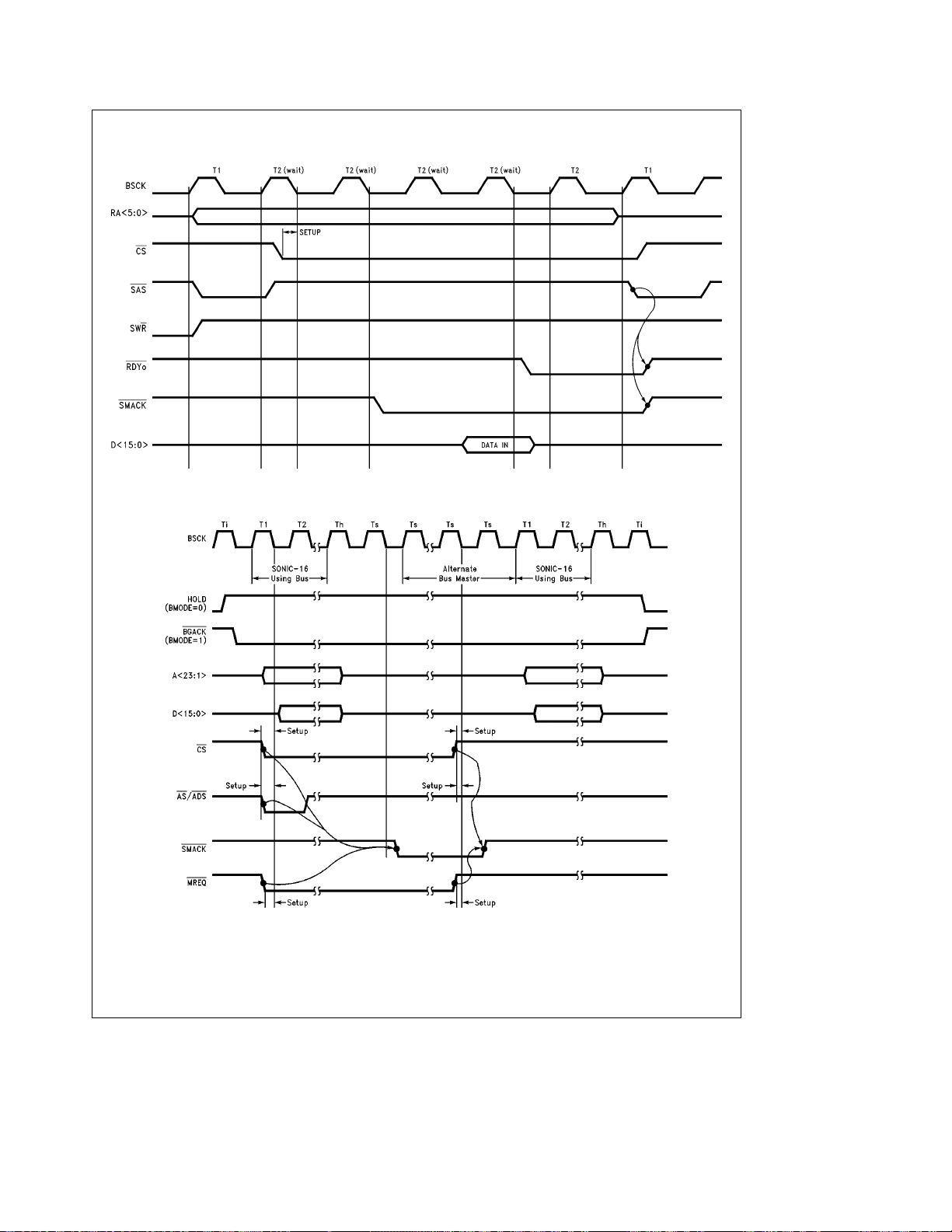
5.0 Bus Interface (Continued)
FIGURE 5-24. Register Write, BMODEe0
FIGURE 5-25. On-Chip Memory Arbiter
TL/F/11722– 50
TL/F/11722– 51
66
Page 67

5.0 Bus Interface (Continued)
5.4.8 On-Chip Memory Arbiter
For applications which share the buffer memory area with
the host system (shared-memory applications), the SONIC16 provides a fast on-chip memory arbiter for efficiently resolving accesses between the SONIC-16 and the host system (
Figure 5-25
to use the shared-memory by asserting Memory Request
(MREQ
). The SONIC-16 will allow the host system to use
the shared memory by acknowledging the host system’s request with Slave and Memory Acknowledge (SMACK
Once SMACK
shared memory freely. The host system gives up the shared
memory by deasserting MREQ
MREQ is clocked in on the falling edge of bus clock and is
double synchronized internally to the rising edge. SMACK
asserted on the falling edge of a Ts bus cycle. If the SONIC16 is not currently accessing the memory, SMACK
ed immediately after MREQ
SONIC-16 is accessing the shared memory, it finishes its
current memory transfer and then issues SMACK
will be asserted 1 or 5 (see Note 2 below) bus clocks, respectively, after MREQ
synchronized, it is not necessary to meet its setup time.
Meeting the setup time for MREQ
that SMACK
the current bus clock. SMACK
clock after MREQ
finish its master operation if it was using the bus previously.
If the host system needs to access the SONIC-16’s registers instead of shared memory, CS
stead of MREQ
almost exactly the same as accessing the shared memory
except that the SONIC-16 goes into a slave cycle instead of
going idle. See Section 5.4.7 for more information about
how register accesses work.
Note 1: The successive assertion of CS and MREQ must be separated by
at least two bus clocks. Both CS
concurrently.
Note 2: The number of bus clocks between MREQ
assertion of SMACK
clocks assuming there were no wait states in the Master Mode
access. Wait states will increase the time for SMACK
the number of wait states in the cycle (the time will be 5
number of wait states).
Note 3: The way in which SMACK
as the way in which SMACK
goes low as a direct result of the assertion of MREQ, whereas, for
CS
0) before SMACK will be asserted. This means that when SMACK
is asserted due to MREQ, SMACK will remain asserted until MREQ
is deasserted. Multiple memory accesses can be made to the
shared memory without SMACK
asserted due to CS
as SAS
will not remain low throughout multiple register accesses to the
SONIC-16 because SAS
is an important difference to consider when designing shared memory designs.
). The host system indicates its intentions
is asserted, the host system may use the
.
is assert-
was clocked in. If, however, the
. SMACK
is clocked in. Since MREQ is double
will, however, guarantee
is asserted in the next or fifth bus clock after
will deassert within one bus
is deasserted. The SONIC-16 will then
would be asserted in-
. Accessing the SONIC-16’s registers works
and MREQ must not be asserted
when the SONIC-16 is in Master Mode is 5 bus
is asserted to due to CS is not the same
is asserted due to MREQ. SMACK
, SAS must also be driven low (BMODEe1) or high (BMODE
, however, SMACK will only remain low as long
is also low (BMODEe1) or high (BMODEe0). SMACK
must toggle for each register access. This
being asserted and the
to go low by
a
ever going high. When SMACK is
the
TABLE 5-4. Internal Register Content after Reset
Contents after Reset
Register
Hardware Software
Reset Reset
Command 0094h 0094h/00A4h
Data Configuration
(DCR and DCR2)
).
Interrupt Mask 0000h unchanged
* unchanged
Interrupt Status 0000h unchanged
Transmit Control 0101h unchanged
Receive Control ** unchanged
is
End Of Buffer Count 02F8h unchanged
Sequence Counters 0000h unchanged
CAM Enable 0000h unchanged
*Bits 15 and 13 of the DCR and bits 4 through 0 of the DCR2 are reset to a 0
during a hardware reset. Bits 15-12 of the DCR2 are unknown until written
to. All other bits in these two registers are unchanged.
**Bits LB1, LB0 and BRD are reset to a 0 during hardware reset. All other
bits are unchanged.
5.4.9 Chip Reset
The SONIC-16 has two reset modes; a hardware reset and
a software reset. The SONIC-16 can be hardware reset by
asserting the RESET
pin or software reset by setting the
RST bit in the Command Register (Section 4.3.1). The two
reset modes are not interchangeable since each mode performs a different function.
After power-on, the SONIC-16 must be hardware reset before it will become operational. This is done by asserting
RESET
for a minimum of 10 transmit clocks (10 Ethernet
transmit clock periods, TXC). If the bus clock (BSCK) period
is greater than the transmit clock period, RESET
asserted for 10 bus clocks instead of 10 transmit clocks. A
hardware reset places the SONIC-16 in the following state.
(The registers affected are listed in parentheses. See Table
5-4 and section 4.3 for more specific information about the
registers and how they are affected by a hardware reset.
Only those registers listed below and in Table 5-4 are affected by a hardware reset.)
1. Receiver and Transmitter are disabled (CR).
2. The General Purpose timer is halted (CR).
e
3. All interrupts are masked out (IMR).
4. The NCRS and PTX status bits in the Transmit Control
Register (TCR) are set.
5. The End Of Byte Count (EOBC) register is set to 02F8h
(760 words).
6. Packet and buffer sequence number counters are set to
zero.
7. All CAM entries are disabled. The broadcast address is
also disabled (CAM Enable Register and the RCR).
8. Loopback operation is disabled (RCR).
9. The latched bus retry is set to the unlatched mode
(DCR).
10. All interrupt status bits are reset (ISR).
11. The Extended Bus Mode is disabled (DCR).
12. HOLD will be asserted/deasserted from the falling
clock edge (DCR2).
should be
67
Page 68

5.0 Bus Interface (Continued)
13. PCOMP
14. Packets will be accepted (not rejected) on CAM match
A software reset immediately terminates DMA operations
and future interrupts. The chip is put into an idle state where
registers can be accessed, but the SONIC-16 will not be
active in any other way. The registers are affected by a
software reset as shown in Table 5-4 (only the Command
Register is changed).
will not be asserted (DCR2).
(DCR2).
6.0 Network Interfacing
The SONIC-16 contains an on-chip ENDEC that performs
the network interfacing between the AUI (Attachment Unit
Interface) and the SONIC-16’s MAC unit. A pin selectable
option allows the internal ENDEC to be disabled and the
MAC/ENDEC signals to be supplied to the user for connection to an external ENDEC. If the EXT pin is tied to ground
e
(EXT
0) the internal ENDEC is selected and if EXT is tied
to V
(EXTe1) the external ENDEC option is selected.
CC
Internal ENDEC: When the internal ENDEC is used
e
(EXT
0) the interface signals between the ENDEC and
MAC unit are internally connected. While these signals are
used internally by the SONIC-16 they are also provided as
an output to the user
The internal ENDEC allows for a 2-chip solution for the
complete Ethernet interface.
gram of the network interface.
(Figure 6-1).
Figure 6-2
shows a typical dia-
FIGURE 6-1. MAC and Internal ENDEC Interface Signals
68
TL/F/11722– 52
Page 69

6.0 Network Interfacing (Continued)
TL/F/11722– 53
0, Using a Single Jumper, JB1, for Network Interface Selection)
e
FIGURE 6-2. Network Interface Example (EXT
69
Page 70

6.0 Network Interfacing (Continued)
e
External ENDEC: When EXT
passed and the signals are provided directly to the user.
Since SONIC-16’s on-chip ENDEC is the same as National’s DP83910 Serial Network Interface (SNI) the interface
considerations discussed in this section would also apply to
using this device in the external ENDEC mode.
6.1 MANCHESTER ENCODER AND
DIFFERENTIAL DRIVER
The ENDEC unit’s encoder begins operation when the MAC
section begins sending the serial data stream. It converts
NRZ data from the MAC section to Manchester data for the
differential drivers (TX
first half of the bit cell contains the complementary data and
the second half contains the true data
sition always occurs at the middle of the bit cell. As long as
the MAC continues sending data, the ENDEC section remains in operation. At the end of transmission, the last transition is always positive, occurring at the center of the bit
cell if the last bit is a one, or at the end of the bit cell if the
last bit is a zero.
The differential transmit pair drives up to 50 meters of twisted pair AUI cable. These outputs are source followers which
require two 270X pull-down resistors to ground. In addition,
a pulse transformer is required between the transmit pair
output and the AUI interface.
The driver allows both half-step and full-step modes for
compatibility with Ethernet I and IEEE 802.3. When the SEL
pin is tied to ground (for Ethernet I), TX
respect to TX
tion transformer (
IEEE 802.3), TX
b
during idle on the primary side of the isola-
Figure 6-2
a
and TXbare equal in the idle state.
FIGURE 6.3. Manchester Encoded Data Stream
6.1.1 Manchester Decoder
The decoder consists of a differential receiver and a phase
lock loop (PLL) to separate the Manchester encoded data
stream into clock signals and NRZ data. The differential input must be externally terminated with two 39X resistors
connected in series. In addition,
quired between the receive input pair and the AUI interface.
To prevent noise from falsely triggering the decoder, a
squelch circuit at the input rejects signals with a magnitude
1 the internal ENDEC is by-
a/b
). In Manchester encoding, the
(Figure 6-3)
a
is positive with
). When SEL is tied to VCC(for
a pulse transformer is re-
. A tran-
TL/F/11722– 54
less than
b
175 mV. Signals more negative thanb300 mV
are decoded.
Once the input exceeds the squelch requirements, the decoder begins operation. The decoder may tolerate bit jitter
up to 18 ns in the received data. The decoder detects the
end of a frame within one and a half bit times after the last
bit of data.
6.1.2 Collision Translator
When the Ethernet transceiver (DP8392 CTI) detects a collision, it generates a 10 MHz signal to the differential collision
inputs (CD
a
and CDb) of the SONIC-16. When SONIC-16
detects these inputs active, its Collision translator converts
the 10 MHz signal to an active collision signal to the MAC
section. This signal causes SONIC-16 to abort its current
transmission and reschedule another transmission attempt.
The collision differential inputs are terminated the same way
as the differential receive inputs and a pulse transformer is
required between the collision input pair and the AUI interface. The squelch circuitry is also similar, rejecting pulses
with magnitudes less than
b
175 mV.
6.1.3 Oscillator Inputs
The oscillator inputs to the SONIC-16 (X1 and X2) can be
driven with a parallel resonant crystal or an external clock.
In either case the oscillator inputs must be driven with a
20 MHZ signal. The signal is divided by 2 to generate the
10 MHz transmit clock (TXC) for the MAC unit. The oscillator also provides internal clock signals for the encoding and
decoding circuits.
6.1.3.1 External Crystal
According to the IEEE 802.3 standard, the transmit clock
(TXC) must be accurate to 0.01%. This means that the oscillator circuit, which includes the crystal and other parts
involved must be accurate to 0.01% after the clock has
been divided in half. Hence, when using a crystal, it is necessary to consider all aspects of the crystal circuit. An example of a recommended crystal circuit is shown in
6-4
and suggested oscillator specifications are shown in Ta-
ble 6-1. The load capacitors in
Figure 6-4
Figure
, C1 and C2,
should be no greater than 36 pF each, including all stray
capacitance (see note 2 below). The resistor, R1, may be
required in order to minimize frequency drift due to changes
in V
. If R1 is required, its value must be carefully selected
CC
since R1 decreases the loop gain. If R1 is made too large,
the loop gain will be greatly reduced and the crystal will not
oscillate. If R1 is made too small, normal variations in V
may cause the oscillation frequency to drift out of specification. As a first rule of thumb, the value of R1 should be
made equal to five times the motional resistance of the crystal. The motional resistance of 20 MHz crystals is usually in
the range of 10X to 30X. This implies that reasonable values for R1 should be in the range of 50X to 150X. The
decision of whether or not to include R1 should be based
upon measured variations of crystal frequency as each of
the circuit parameters are varied.
CC
70
Page 71

6.0 Network Interfacing (Continued)
output drive specification need only be one CMOS load.
This circuit configuration also offers the advantage of slightly lower power consumption. In this configuration, the X1 pin
must be left open and should not drive external circuitry.
Also, as shown by
Figure 6-6
, there is a 180§phase difference between connecting an oscillator to X1 compared to
X2. This difference only affects the relationship between
TXC and the oscillator module output. The operation of the
SONIC-16 is not affected by this phase change.
FIGURE 6.4. Crystal Connection
TL/F/11722– 55
to the SONIC-16 (see text)
Note 1: The X1 pin is not guaranteed to provide a TTL compatible logic
output, and should not be used to drive any external logic. If additional logic needs to be driven, then an external oscillator should be
used as described in the following section.
Note 2: The frequency marked on the crystal is usually measured with a
fixed load capacitance specified in the crystal’s data sheet. The
actual load capacitance used should be the specified value minus
the stray capacitance.
TABLE 6-1. Crystal Specifications
Resonant frequency 20 MHz
Tolerance (see text)
Accuracy
g
0.005% (50 ppm) at 0 to 70§C
Fundamental Mode Series Resistance
Specified Load Capacitance
g
0.01% at 25§C
s
s
25X
18 pF
Type AT cut
Circuit Parallel Resonance
6.1.3.2 Clock Oscillator Module
If an external clock oscillator is used, the SONIC-16 can be
connected to the external oscillator in one of two ways. The
first configuration is shown in
Figure 6-5
. In this case, an
oscillator that provides the following should be used:
1. TTL or CMOS output with a 0.01% frequency tolerance
2. 40% –60% duty cycle
t
3.
5 TTL loads output drive (I
put drive may be necessary if the oscillator must also
e
8 mA) (Additional out-
OL
drive other components.)
Again, the above assumes no other circuitry is driven.
FIGURE 6.5. Oscillator Module
TL/F/11722– 56
Connection to the SONIC-16
The second configuration, shown in
Figure 6-6
, connects to
the X2 input. This connection requires an oscillator with the
same specifications as the previous circuit except that the
FIGURE 6.6. Alternate Oscillator
TL/F/11722– 57
Module Connection to the SONIC-16
6.1.3.3 PCB Layout Considerations
Care should be taken when connecting a crystal. Stray capacitance (e.g., from PC board traces and plated through
holes around the X1 and X2 pins) can shift the crystal’s
frequency out of range, causing the transmitted frequency
to exceed the 0.01% tolerance specified by IEEE. The layout considerations for using an external crystal are rather
straightforward. The oscillator layout should locate all components close to the X1 and X2 pins and should use short
traces that avoid excess capacitance and inductance. A solid ground should be used to connect the ground legs of the
two capacitors.
When connecting an external oscillator, the only considerations are to keep the oscillator module as close to the
SONIC-16 as possible to reduce stray capacitance and inductance and to give the module a clean V
ground.
and a solid
CC
6.1.4 Power Supply Considerations
In general, power supply routing and design for the SONIC16 need only follow standard practices. In some situations,
however, additional care may be necessary in the layout of
the analog supply. Specifically special care may be needed
for the TXVCC, RXVCC and PLLVCC power supplies and
the TXGND and ANGND. In most cases the analog and
digital power supplies can be interconnected. However, to
ensure optimum performance of the SONIC-16’s analog
functions, power supply noise should be minimized. To reduce analog supply noise, any of several techniques can be
used.
1. Route analog supplies as a separate set of traces or
planes from the digital supplies with their own decoupling
capacitors.
2. Provide noise filtering on the analog supply pins by inserting a low pass filter. Alternatively, a ferrite bead could be
used to reduce high frequency power supply noise.
3. Utilize a separate regulator to generate the analog supply.
71
Page 72

7.0 AC and DC Specifications
Absolute Maximum Ratings
If Military/Aerospace specified devices are required,
please contact the National Semiconductor Sales
Office/Distributors for availability and specifications.
Supply Voltage (V
DC Input Voltage (V
DC Output Voltage (V
CC
)
)
IN
)
OUT
DC Specifications T
e
A
b
b
b
0.5V to 7.0V
0.5V to V
0.5V to V
0§Cto70§C, V
CC
CC
CC
a
0.5V
a
0.5V
e
5Vg5% unless otherwise specified
Storage Temperature Range (T
STG
Power Dissipation (PD) 500 mW
Lead Temp. (TL) (Soldering, 10 sec.) 260§C
ESD Rating
e
(R
1.5k, C
ZAP
e
120 pF) 1.5 KV
ZAP
Symbol Parameter Conditions Min Max Units
V
OH
V
OL
V
IH
V
IL
I
IN
I
OZ
I
CC
Minimum High Level Output Voltage I
Maximum Low Level Output Voltage I
Minimum High Level Input Voltage 2.0 V
Maximum Low Level Input Voltage 0.8 V
Input Current V
Maximum TRI-STATE Output V
Leakage Current
Average Operating Supply Current I
eb
8 mA 3.0 V
OH
e
8 mA 0.4 V
OL
IN
OUT
OUT
e
e
VCCor GND
e
VCCor GND
0 mA, Freqef
max
b
1.0 1.0 mA
b
10 10 mA
AUI INTERFACE PINS (TXg,RXg, and CDg)
V
OD
V
OB
V
U
V
DS
Diff. Output Voltage (TXg)78XTermination, and 270X
from Each to GND
Diff. Output Voltage Imbalance (TXg)78XTermination, and 270X
from Each to GND
Undershoot Voltage (TXg)78XTermination, and 270X
from Each to GND
Diff. Squelch Threshold
g
and CDg)
(RX
g
550
b
175
OSCILLATOR PINS (X1 AND X2)
V
IH
V
IL
I
OSC1
V
IH
V
IL
I
OSC2
X1 Input High Voltage X1 is Connected to an Oscillator
and X2 is Grounded
X1 Input Low Voltage X1 is Connected to an Oscillator
and X2 is Grounded
X1 Input Current X1 is Connected to an Oscillator
and X2 is Grounded 8 mA
e
V
VCCor GND
IN
X2 Input High Voltage X2 is Connected to an Oscillator
and X1 is Open
X2 Input Low Voltage X2 is Connected to an Oscillator
and X1 is Open
X2 Input Leakage Current X2 is Connected to an Oscillator
and X1 is Open
e
V
VCCor GND
IN
2.0 V
2.0 V
b
10 10 mA
b
)
80 mA
g
1200 mV
Typical: 40 mV
Typical: 80 mV
b
300 mV
0.8 V
0.8 V
65§Cto150§C
72
Page 73

7.0 AC and DC Specifications (Continued)
AC Specifications
BUS CLOCK TIMING
TL/F/11722– 58
Number Parameter
20 MHz
Min Max
Units
T1 Bus Clock Low Time 22.5 ns
T2 Bus Clock High Time 22.5 ns
T3 Bus Clock Cycle Time (Note 2) 50 100 ns
POWER-ON RESET
TL/F/11722– 59
NON POWER-ON RESET
TL/F/11722– 60
Number Parameter
20 MHz
Min Max
Units
T4 USRk1:0lSetup to RST 10 ns
T5 USRk1:0lHold from RST 20 ns
T6 Power-On Reset High (Notes 1, 2) 10 TXC
T8 Reset Pulse Width (Notes 1, 2) 10 TXC
Note 1: The reset time is determined by the slower of BSCK or TXC. If BSCKlTXC, T6 and T8 equal 10 TXCs. If BSCKkTXC, T6 and T8 equal 10 BSCKs (T3).
Note 2: These specifications are not tested.
73
Page 74

7.0 AC and DC Specifications (Continued)
MEMORY WRITE, BMODE
e
0, SYNCHRONOUS MODE (one wait-state shown)
TL/F/11722– 61
Number Parameter
20 MHz
Min Max
Units
T9 BSCK to Address Valid 34 ns
T10 Address Hold Time from BSCK 5 ns
T11 BSCK to ADS, ECS Low 34 ns
T12 BSCK to ADS, ECS High 34 ns
T15 ADS High Width (Note 2) bcyc-5 ns
T32 RDYi Setup to BSCK 30 ns
T33 RDYi Hold from BSCK 5 ns
T36 BSCK to Memory Write Data Valid 70 ns
T37 BSCK to MWR (Write) Valid (Note 1) 30 ns
T40 Write Data Hold Time from BSCK 10 ns
Note 1: For successive read operations, MWR remains low, and for successive write operations, MWR remains high during a transfer. During RDA and TDA
transfers the MWR
of a Ti (idle) state that is inserted between the read and the write operation.
Note 2: bcyc
signal will stay either high or low for the entire burst of the transfer. During RDA and TDA transfers the MWR signal will switch on the rising edge
e
bus clock cycle time (T3).
74
Page 75

7.0 AC and DC Specifications (Continued)
MEMORY READ, BMODE
e
0, SYNCHRONOUS MODE (one wait-state shown)
TL/F/11722– 62
Number Parameter
20 MHz
Min Max
Units
T9 BSCK to Address Valid 34 ns
T10 Address Hold Time from BSCK 5 ns
T11 BSCK to ADS, ECS Low 34 ns
T12 BSCK to ADS, ECS High 34 ns
T15 ADS High Width (Note 2) bcycb5ns
T23 Read Data Setup Time to BSCK 12 ns
T24 Read Data Hold Time from BSCK 7 ns
T28 BSCK to MWR (Read) Valid (Note 1) 30 ns
T32 RDYi Setup Time to BSCK 30 ns
T33 RDYi Hold Time to BSCK 5 ns
Note 1: For successive read operations, MWR remains low, and for successive write operations, MWR remains high. During RBA and TBA transfers the MWR
signal will stay either high or low for the entire burst of the transfer. During RDA and TDA transfers, the MWR signal will switch on the rising edge of a Ti (idle) state
that is inserted between the read and the write operation.
Note 2: bcyc
e
bus clock cycle time (T3).
75
Page 76
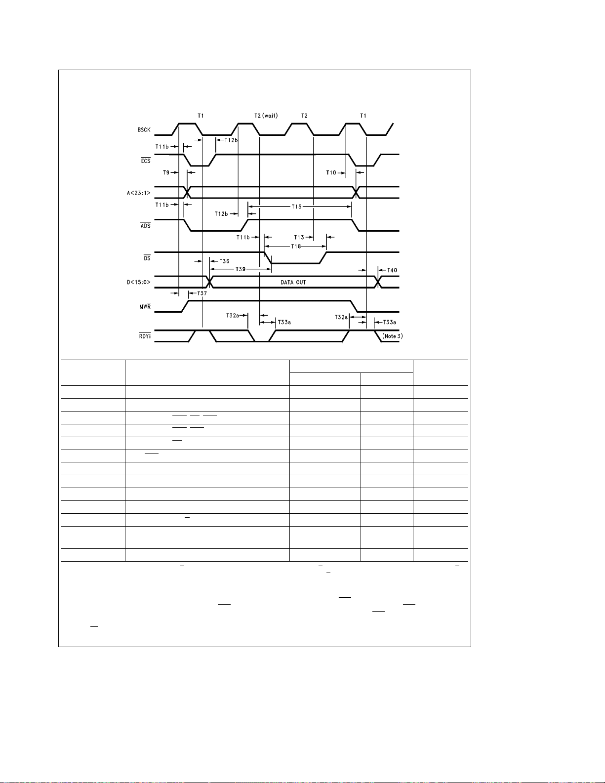
7.0 AC and DC Specifications (Continued)
MEMORY WRITE, BMODE
e
0, ASYNCHRONOUS MODE
TL/F/11722– 63
Number Parameter
20 MHz
Min Max
Units
T9 BSCK to Address Valid 34 ns
T10 Address Hold Time from BSCK 5 ns
T11b BSCK to ADS,DS, ECS Low 30 ns
T12b BSCK to ADS, ECS High 32 ns
T13 BSCK to DS High 36 ns
T15 ADS High Width (Note 2) bcycb5ns
T18 Write Data Strobe Low Width (Notes 2, 4) bcycb5ns
T32a Ready Asynch. Setup to BSCK (Note 3) 8 ns
T33a Ready Asynch. Hold from BSCK 5 ns
T36 BSCK to Memory Write Data Valid 70 ns
T37 BSCK to MWR (Write) Valid (Note 1) 30 ns
T39 Write Data Valid to
Data Strobe Low (Note 2)
b
bcyc
40 ns
T40 Write Data Hold Time from BSCK 10 ns
Note 1: For successive read operations, MWR
signal will stay either high or low for the entire burst of the transfer. During RDA and TDA transfers, the MWR signal will switch on the rising edge of a Ti (idle) state
that is inserted between the read and the write operation.
Note 2: bcyc
Note 3: This setup time assures that the SONIC-16 terminates the memory cycle on the next bus clock (BSCK). RDYi
clock, though, since it is an asynchronous input in this case. RDYi
cycle, the SONIC-16 will finish the current access in a total of two bus clocks instead of three, which would be the case if RDYi
T2(wait). (This is assuming that programmable wait states are set to 0).
Note 4: DS
e
bus clock cycle time (T3)
will only be asserted if the bus cycle has at least one wait state inserted.
remains low, and for successive write operations, MWR remains high. During RBA and TBA transfers the MWR
is sampled during the falling edge of BSCK. If the SONIC-16 samples RDYi low during the T1
does not need to be synchronized to the bus
had been sampled low during
76
Page 77

7.0 AC and DC Specifications (Continued)
MEMORY READ, BMODE
e
0, ASYNCHRONOUS MODE
TL/F/11722– 64
Number Parameter
20 MHz
Min Max
Units
T9 BSCK to Address Valid 34 ns
T10 Address Hold Time from BSCK 5 ns
T11b BSCK to ADS,DS, ECS Low 30 ns
T12b BSCK to ADS,DS, ECS High 32 ns
T13 BSCK to DS High 36 ns
T15 ADS High Width (Note 2) bcycb5ns
T16 Read Data Strobe High Width (Note 2) bcycb12 ns
T17 Read Data Strobe Low Width (Note 2) bcycb5ns
T23 Read Data Setup Time to BSCK 12 ns
T24 Read Data Hold Time from BSCK 7 ns
T28 BSCK to MWR (Read) Valid (Note 1) 30 ns
T32a Ready Asynch. Setup Time to BSCK (Note 3) 8 ns
T33a Ready Asynch. Hold Time to BSCK 5 ns
Note 1: For successive read operations, MWR remains low, and for successive write operations, MWR remains high. During RBA and TBA transfers the MWR
signal will stay either high or low for the entire burst of the transfer. During RDA and TDA transfers, the MWR signal will switch on the rising edge of a Ti (idle) state
that is inserted between the read and the write operation.
Note 2: bcyc
Note 3: This setup time assures that the SONIC-16 terminates the memory cycle on the next bus clock (BSCK). RDYi
clock, though, since it is an asynchronous input in this case. RDYi
cycle, the SONIC-16 will finish the current access in a total of two bus clocks instead of three, which would be the case if RDYi
T2(wait). (This is assuming that programmable wait states are set to 0).
e
bus clock cycle time (T3)
is sampled during the falling edge of BSCK. If the SONIC-16 samples RDYi low during the T1
does not need to be synchronized to the bus
had been sampled low during
77
Page 78

7.0 AC and DC Specifications (Continued)
MEMORY WRITE, BMODE
e
1, SYNCHRONOUS MODE (one wait-state shown)
TL/F/11722– 65
Number Parameter
20 MHz
Min Max
Units
T9 BSCK to Address Valid 34 ns
T10 Address Hold Time from BSCK 5 ns
T11a BSCK to AS,DS, ECS Low 26 ns
T12a BSCK to AS
, ECS High 34 ns
T13a BSCK to DS High 36 ns
T14 AS Strobe Low Width (Note 3) bcycb7ns
T15a AS Strobe High Width (Note 3) bcycb15 ns
T18 Write Data Strobe Low Width (Notes 1, 3) bcycb5ns
T22 Address Valid to AS (Note 3) bchb18 ns
T30 DSACK0,1 Setup to BSCK (Note 4) 8 ns
T31 DSACK0,1 Hold from BSCK 12 ns
T36 BSCK to Memory Write Data Valid 70 ns
T37 BSCK to MRW (Write) Valid (Note 2) 30 ns
T39 Write Data Valid to
Data Strobe Low (Note 3)
b
bcyc
40 ns
T40 Memory Write Data Hold Time from BSCK 10 ns
Note 1: DS will only be asserted if the bus cycle has at least one wait state inserted.
Note 2: For successive read operations, MWR
signal will stay either high or low for the entire burst of the transfer. During RDA and TDA transfers, the MWR signal will switch on the rising edge of a Ti (idle) state
that is inserted between the read and the write operation.
Note 3: bcyc
Note 4: DSACK0,1
e
bus clock cycle time (T3). bchebus clock high time (T2).
must be synchronized to the bus clock (BSCK) during synchronous mode.
remains low, and for successive write operations, MWR remains high. During RBA and TBA transfers the MWR
78
Page 79

7.0 AC and DC Specifications (Continued)
MEMORY READ, BMODE
e
1, SYNCHRONOUS MODE (one wait-state shown)
TL/F/11722– 66
Number Parameter
20 MHz
Min Max
Units
T9 BSCK to Address Valid 34 ns
T10 Address Hold Time from BSCK 5 ns
T11a BSCK to AS
,DS, ECS Low 26 ns
T12a BSCK to AS, ECS High 34 ns
T13a BSCK to DS High 36 ns
T14 AS Strobe Low Width (Note 3) bcycb7ns
T15a AS Strobe High Width (Note 3) bcycb15 ns
T16 Read Data Strobe High Width (Note 3) bcycb12 ns
T17 Read Data Strobe Low Width (Note 3) bcycb5ns
T22 Address Valid to AS (Note 3) bchb18 ns
T23a Read Data Setup Time to BSCK 5 ns
T24a Read Data Hold Time from BSCK 5 ns
T28 BSCK to MRW (Read) Valid (Note 1) 30 ns
T30 DSACK0,1 Setup to BSCK (Note 2) 8 ns
T31 DSACK0,1 Hold from BSCK 12 ns
Note 1: For successive read operations, MWR remains low, and for successive write operations, MWR remains high. During RBA and TBA transfers the MWR
signal will stay either high or low for the entire burst of the transfer. During RDA and TDA transfers, the MWR signal will switch on the rising edge of a Ti (idle) state
that is inserted between the read and the write operation.
Note 2: DSACK0,1
Note 3: bcyc
must be synchronized to the bus clock (BSCK) during synchronous mode.
e
bus clock cycle time (T3). bchebus clock high time (T2)
79
Page 80

7.0 AC and DC Specifications (Continued)
MEMORY WRITE, BMODE
e
1, ASYNCHRONOUS MODE
TL/F/11722– 67
Number Parameter
20 MHz
Min Max
Units
T9 BSCK to Address Valid 34 ns
T10 Address Hold Time from BSCK 5 ns
T11a BSCK to AS,DS, ECS Low 26 ns
T12a BSCK to AS, ECS High 34 ns
T13a BSCK to DS High 36 ns
T14 AS Strobe Low Width (Note 3) bcycb7ns
T15a AS Strobe High Width (Note 3) bcycb15 ns
T18 Write Data Strobe Low Width (Notes 3, 4) bcycb5ns
T22 Address Valid to AS (Note 3) bchb18 ns
T30 DSACK0,1 Setup to BSCK (Note 2) 8 ns
T30a STERM Setup to BSCK (Note 2) 6 ns
T31 DSACK0,1 Hold from BSCK 12 ns
T31a STERM Hold from BSCK 12 ns
T36 BSCK to Memory Write Data Valid 70 ns
T37 BSCK to MRW (Write) Valid (Note 1) 30 ns
T39 Write Data Valid to Data Strobe Low (Note 3) bcycb40 ns
T40 Memory Write Data Hold from BSCK 10 ns
Note 1: For successive read operations, MWR remains low, and for successive write operations, MWR remains high. During RBA and TBA transfers the MWR
signal will stay either high or low for the entire burst of the transfer. During RDA and TDA transfers, the MWR signal will switch on the rising edge of a Ti (idle) state
that is inserted between the read and the write operation.
Note 2: Meeting the setup time for DSACK0,1
sampled, or 1 cycle after STERM
or STERM low during the T1 or first T2 state respectively, the SONIC-16 will finish the current access in a total of two bus clocks instead of three
DSACK0,1
(assuming that programmable wait states are set to 0). DSACK0,1
Note 3: bcyc
Note 4: DS
e
bus clock cycle time (T3). bchebus clock high time (T2).
will only be asserted if the bus cycle has at least one wait state inserted.
was sampled. T2 states will be repeated until DSACK0,1 or STERM are sampled properly in a low state. If the SONIC-16 samples
or STERM guarantees that the SONIC-16 will terminate the memory cycle 1(/2 bus clocks after DSACK0,1 were
are asynchronously sampled and STERM is synchronously sampled.
80
Page 81
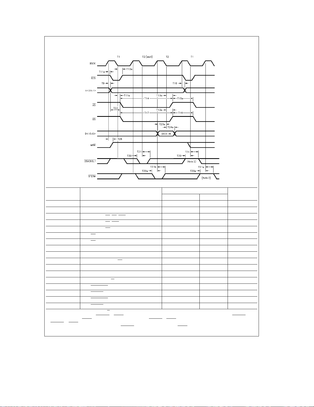
7.0 AC and DC Specifications (Continued)
MEMORY READ, BMODE
e
1, ASYNCHRONOUS MODE
TL/F/11722– 68
Number Parameter
20 MHz
Min Max
Units
T9 BSCK to Address Valid 34 ns
T10 Address Hold Time from BSCK 5 ns
T11a BSCK to AS,DS, ECS Low 26 ns
T12a BSCK to AS, ECS High 34 ns
T13a BSCK to DS High 36 ns
T14 AS Strobe Low Width (Note 3) bcycb7ns
T15a AS Strobe High Width (Note 3) bcycb15 ns
T16 Read Data Strobe High Width (Note 3) bcycb12 ns
T17 Read Data Strobe Low Width (Note 3) bcycb5ns
T22 Address Valid to AS (Note 3) bchb18 ns
T23a Read Data Setup Time to BSCK 10 ns
T24a Read Data Hold Time from BSCK 5 ns
T28 BSCK to MRW (Read) Valid (Note 1) 30 ns
T30 DSACK0,1 Setup to BSCK (Note 2) 8 ns
T30a STERM Setup to BSCK (Note 2) 6 ns
T31 DSACK0,1 Hold from BSCK 12 ns
T31a STERM Hold from BSCK 12 ns
Note 1: For successive write operations, MRW remains low.
Note 2: Meeting the setup time for DSACK0,1
sampled, or 1 cycle after STERM
or STERM low during the T1 or first T2 state respectively, the SONIC-16 will finish the current access in a total of two bus clocks instead of three
DSACK0,1
(assuming that programmable wait states are set to 0). DSACK0,1
Note 3: bcyc
e
bus clock cycle time (T3). bchebus clock high time (T2).
was sampled. T2 states will be repeated until DSACK0,1 or STERM are sampled properly in a low state. If the SONIC-16 samples
or STERM guarantees that the SONIC-16 will terminate the memory cycle 1(/2 bus clocks after DSACK0,1 were
are asynchronously sampled and STERM is synchronously sampled.
81
Page 82

7.0 AC and DC Specifications (Continued)
BUS REQUEST TIMING, BMODE
e
0
TL/F/11722– 69
Number Parameter
20 MHz
Min Max
Units
T43 BSCK to HOLD High (Note 2) 25 ns
T44 BSCK to HOLD Low (Note 2) 22 ns
T45 HLDA Asynchronous Setup Time to BSCK 5 ns
T46 HLDA Deassert Setup Time (Note 1) 5 ns
T51 BSCK to Address, ADS, MWR,DS, ECS,
k
USR
1:0land EXUSRk3:0lTRI-STATE 52 ns
(Note 4)
T52 BSCK to Data TRI-STATE (Note 4) 68 ns
T53 BSCK to USRk1:0lValid 50 ns
T55 BSCK to Bus Status
Idle to Non-Idle
T55a BSCK to Bus Status
Non-Idle to Idle (Note 3)
40 ns
40 ns
T55b Sk2:0lHold from BSCK 10 ns
Note 1: A block transfer by the SONIC-16 can be pre-empted from the bus by deasserting HLDA provided HLDA is asserted T46 before the rising edge of the last
T2 in the current access.
Note 2: The assertion edge for HOLD is dependent upon the PH bit in the DCR2. The default situation is shown wih a solid line in the timing diagram. T43 and T44
apply for both modes. Also, if HLDA is asserted when the SONIC-16 wants to acquire the bus, HOLD will not be asserted until HLDA has been deasserted first.
k
Note 3: S
2:0lwill indicate IDLE at the end of T2 if the last operation is a read operation, or at the end of Th if the last operation is a write operation.
Note 4: This timing value includes an RC delay inherent in the test measurement. These signals typically TRI-STATE 7 ns earlier, enabling other devices to drive
these lines without contention.
Note 5: For specific timings on these signals (driven by the SONIC-16), see the memory read and memory write timing diagrams on previous pages.
82
Page 83

7.0 AC and DC Specifications (Continued)
BUS REQUEST TIMING, BMODE
e
1
TL/F/11722– 70
Number Parameter
20 MHz
Min Max
Units
T45a BG Asynchronous Setup Time to BSCK 8 ns
T47 BSCK Low to BR Low 25 ns
T48 BSCK Low to BR
TRI-STATE (Note 4) 30 ns
T49 BSCK High to BGACK Low (Note 1) 30 ns
T50 BSCK High to BGACK High (Note 5) 30 ns
T51a BSCK to Address, AS, MRW,DS, ECS,
k
USR
1:0land EXUSRk3:0lTRI-STATE (Note 4)
52 ns
T52 BSCK to Data TRI-STATE (Note 4) 68 ns
T53 BSCK to USRk1:0lValid 50 ns
T55 BSCK to Bus Status
Idle to Non-Idle
T55a BSCK to Bus Status
Non-Idle to Idle (Note 3)
40 ns
40 ns
T55b Sk2:0lHold from BSCK 10 ns
Note 1: BGACK is only issued if BG is low and AS, DSACK0,1, STERM and BGACK are deasserted.
Note 2: For specific timing on these signals driven by the SONIC-16, see the memory read and memory write timing diagrams on previous pages.
k
Note 3: S
2:0lwill inidicate IDLE at the end of T2 if the last operation is a read operation or at the end of Th if the last operation is a write operation.
Note 4: This timing value includes an RC delay inherent in our test measurement. These signals typically TRI-STATE 7 ns eariler, enabling other devices to drive
these lines without contention.
Note 5: BGACK
is driven high for approximately (/2 BSCK before going TRI-STATE.
83
Page 84

7.0 AC and DC Specifications (Continued)
BUS RETRY
TL/F/11722– 71
Number Parameter
T41 Bus Retry Synchronous Setup Time to BSCK
(Note 3)
T41a Bus Retry Asynchronous
Setup Time to BSCK (Note 3)
20 MHz
Min Max
Units
5ns
5ns
T42 Bus Retry Hold Time from BSCK (Note 2) 7 ns
T43 BSCK to HOLD High (Note 1) 25 ns
T44 BSCK to HOLD Low (Note 1) 22 ns
T47 BSCK to BR Low 25 ns
T50 BSCK to BGACK High (Note 4) 30 ns
Note 1: Depending upon the mode, the SONIC-16 will assert and deassert HOLD from the rising or falling edge of BSCK.
Note 2: Unless Latched Bus Retry mode is set (LBR in the Data Configuration Register, Section 4.3.2), BRT
Latched Bus Retry mode is used, BRT
Note 3: T41 is for synchronous bus retry and T41a is for asynchronous bus retry (see Section 4.3.2, bit 15, Extended Bus Mode). Since T41a is an asynchronous
setup time, it is not necessary to meet it, but doing so will guarantee that the bus exception occurs in the current memory transfer, not the next.
Note 4: BGACK
is driven high for approximately (/2 BSCK before going TRI-STATE.
does not need to satisfy T42.
must remain asserted until after the Th state. If
84
Page 85

7.0 AC and DC Specifications (Continued)
MEMORY ARBITRATION/SLAVE ACCESS
TL/F/11722– 72
Number Parameter
T56 CS Low Asynch. Setup to BSCK
(Note 2)
20 MHz
Min Max
Units
12 ns
T57 CS High Asynch. Setup to BSCK 8 ns
T58 MREQ Low Asynch. Setup to BSCK
(Note 2)
12 ns
T59 MREQ High Asynch. Setup to BSCK 12 ns
T60 MREQ or CS to SMACK Low (Notes 3, 4) 1.5
5.5
bcyc
T80 MREQ to SMACK High 30 ns
T81 BSCK to SMACK Low 25 ns
Note 1: Both CS and MREQ must not be asserted concurrently. If these signals are successively asserted, there must be at least two bus clocks between the
deasserting and asserting edges of these signals.
Note 2: It is not necessary to meet the setup times for MREQ
however, makes it possible to use T60 to determine exactly when SMACK
Note 3: The smaller value for T60 refers to when the SONIC-16 is accessed during an Idle condition and the other value refers to when the SONIC-16 is accessed
during non-idle conditions. These values are not tested, but are guaranteed by design. This specification assumes that CS
the falling edge that these signals are asynchronously clocked in on (see T56 and T58). If T56 is met for CS
exactly 1 bus clock, when the SONIC-16 was idle, or 5 bus clocks, when the SONIC-16 was in master mode, after the edge that T56 and T58 refer to. (This is
assuming that there were no wait states in the current master mode access. Wait states will increase the time for SMACK
the cycle.) SAS
Note 4: bcyc
Note 5: The way in which SMACK
result of the assertion of MREQ
that when SMACK
memory without SMACK
high (BMODE
an important difference to consider when designing shared memory designs.
must have been asserted for this timing to be correct. See SAS and CS timing in the Register Read and Register Write timing specifications.
e
bus clock cycle time (T3).
is asserted due to MREQ, SMACK will remain asserted until MREQ is deasserted. Multiple memory accesses can be made to the shared
e
0). SMACK will not remain low throughout multiple register accesses to the SONIC-16 because SAS must toggle for each register access. This is
is asserted is due to CS is not the same as the way in which SMACK is asserted due to MREQ. SMACK goes low as a direct
, whereas, for CS, SAS must also be driven low (BMODEe1) or high (BMODEe0) before SMACK will be asserted. This means
ever going high. When SMACK is asserted due to CS, however, SMACK will only remain low as long as SAS is also low (BMODEe1) or
or CS since these signals are asynchronously sampled. Meeting the setup time for these signals,
will be asserted.
or T58 is met for MREQ, then SMACK will be asserted
or MREQ is asserted (/2 bus clock before
to go low by the number of wait states in
85
Page 86

7.0 AC and DC Specifications (Continued)
REGISTER READ, BMODE
e
0 (Note 1)
TL/F/11722– 73
Number Parameter
20 MHz
Min Max
Units
T56 CS Asynch. Setup to BSCK (Note 4) 12 ns
T60 MREQ or CS to SMACK Low (Notes 3, 5, 8) 1.5
5.5
bcyc
T62 SAS Assertion before CS (Note 6) 0 ns
T62a SAS Deassertion after CS (Notes 3, 6) 1 bcyc
T63 Register Address Setup to SAS 10 ns
T64 Register Address Hold Time from SAS 10 ns
T65 SAS Pulse Width (Note 3) bcycb10 ns
T68 SWR (Read) Hold from SAS 8ns
T72 SMACK to RDYo Low (Notes 3, 8) 2.5 bcyc
T73 SWR (Read) Setup to SAS 0ns
T75 BSCK to RDYo Low 35 ns
T76 SAS or CS to RDYo High (Note 2) 30 ns
T79 SAS or CS to SMACK High (Note 2) 30 ns
T81 BSCK to SMACK Low 25 ns
T82 BSCK to Register Data Valid 83 ns
T85 SAS or CS to Data TRI-STATE (Notes 2, 7) 60 ns
T85a Min. CS Deassert Time (Note 3) 1 bcyc
Note 1: This figure shows a slave access to the SONIC-16 when the SONIC-16 is idle, or rather not in master mode. If the SONIC-16 is a bus master, there will be
some differences as noted in the Memory Arbitration/Slave Access diagram. The BSCK states (T1, T2, etc.) are the equivalent processor states during a slave
access.
Note 2: If CS
Note 3: bcyc
Note 4: It is not necessary to meet the setup time for CS
possible to use T60 to determine exactly when SMACK
Note 5: The smaller value for T60 refers to when the SONIC-16 is accessed during an Idle condition and the other value refers to when the SONIC-16 is accessed
during non-idle conditions. These values are not tested, but are guaranteed by design. This specification assumes that CS
falling edge that CS
or 5 bus clocks, when the SONIC-16 was in master mode, after the edge that T56 refers to. (This is assuming that there were no wait states in the current master
mode access. Wait states will increase the time for SMACK
Note 6: SAS
however, SAS
Note 7: This timing value includes an RC delay inherent in the test measurement. These signals typically TRI-STATE 7 ns eariler, enabling other devices to drive
these lines without contention.
Note 8: These values are not tested, but are guaranteed by design. They are provided as a design guideline only.
is deasserted before the falling edge of SAS, T76, T79 and T85 are referenced from the rising edge of CS.
e
bus clock cycle time (T3).
is asynchronously clocked in on (see T56). If T56 is met for CS, then SMACK will be asserted exactly 1 bus clock, when the SONIC-16 was idle,
may be asserted low anytime before or simultaneous to the falling edge of CS. It is suggested that SAS be driven high no later than CS. If necessary,
may be driven up to 1 BSCK after CS.
since this signal is asynchronously sampled. Meeting the setup time for this signal, however, makes it
will be asserted.
is asserted (/2 bus clock before the
to go low by the number of wait states in the cycle.)
86
Page 87

7.0 AC and DC Specifications (Continued)
REGISTER WRITE, BMODE
e
0 (Note 1)
TL/F/11722– 74
Number Parameter
20 MHz
Min Max
Units
T56 CS Asynch. Setup to BSCK (Note 4) 12 ns
T60 MREQ or CS to SMACK Low (Notes 3, 5, 7) 1.5
5.5
bcyc
T62 SAS Assertion before CS (Note 6) 0 ns
T62a SAS Deassertion after CS (Notes 3, 6) 1 bcyc
T63 Register Address Setup to SAS 10 ns
T64 Register Address Hold Time from SAS 10 ns
T65 SAS Pulse Width (Note 3) bcycb10 ns
T70 SWR (Write) Setup to SAS 0ns
T71 SWR (Write) Hold from SAS 7ns
T72 SMACK to RDYo Low (Notes 3, 7) 2.5 bcyc
T75 BSCK to RDYo Low 35 ns
T76 SAS or CS to RDYo High (Note 2) 30 ns
T79 SAS or CS to SMACK High (Note 2) 30 ns
T81 BSCK to SMACK Low 25 ns
T83 Register Write Data Setup to BSCK 45 ns
T84 Register Write Data Hold from BSCK 20 ns
T85a Min. CS Deassert Time (Note 3) 1 bcyc
Note 1: This figure shows a slave access to the SONIC-16 when the SONIC-16 is idle, or rather not in master mode. If the SONIC-16 is a bus master, there will be
some differences as noted in the Memory Arbitration/Slave Access diagram. The BSCK states (T1, T2, etc.) are the equivalent processor states during a slave
access.
Note 2: If CS
Note 3: bcyc
Note 4: It is not necessary to meet the setup time for CS
possible to use T60 to determine exactly when SMACK
Note 5: The smaller value for T60 refers to when the SONIC-16 is accessed during an Idle condition and the other value refers to when the SONIC-16 is accessed
during non-idle conditions. These values are not tested, but are guaranteed by design. This specification assumes that CS
falling edge that CS
or 5 bus clocks, when the SONIC-16 was in master mode, after the edge that T56 refers to. (This is assuming that there were no wait states in the current master
mode access. Wait states will increase the time for SMACK
Note 6: SAS
however, SAS
Note 7: These values are not tested, but are guaranteed by design. They are provided as a design guideline only.
is deasserted before the falling edge of SAS, T76 and T79 are referenced from the rising edge of CS.
e
bus clock cycle time (T3).
is asynchronously clocked in on (see T56). If T56 is met for CS, then SMACK will be asserted exactly 1 bus clock, when the SONIC-16 was idle,
may be asserted low anytime before or simultaneous to the falling edge of CS. It is suggested that SAS be driven high no later than CS. If necessary,
may be driven up to 1 BSCK after CS.
since this signal is asynchronously sampled. Meeting the setup time for this signal, however, makes it
will be asserted.
is asserted (/2 bus clock before the
to go low by the number of wait states in the cycle.)
87
Page 88

7.0 AC and DC Specifications (Continued)
REGISTER READ, BMODE
Number Parameter
T56 CS Asynch. Setup to BSCK (Note 5) 12 ns
T60 MREQ or CS to SMACK Low (Notes 4, 6, 9) 1.5
T62 SAS Assertion before CS (Note 7) 0 ns
T63 Register Address Setup to SAS 10 ns
T64 Register Address Hold from SAS 10 ns
T67 SRW (Read) Setup to SAS 0ns
T72a SMACK to DSACK0,1 Low (Notes 4, 9) 2 bcyc
T74 SRW (Read) Hold from SAS 50 ns
T75a BSCK to DSACK0,1 Low 35 ns
T77 CS to DSACK0,1 High (Notes 2, 3) 25 ns
T77a SAS to DSACK0,1 High (Notes 2, 3) 35 ns
T78 Skew between DSACK0,1 10 ns
T79a BSCK to SMACK High 30 ns
T81 BSCK to SMACK Low 25 ns
T82 BSCK to Register Data Valid 83 ns
T85a Min. CS Deassert Time (Note 4) 1 bcyc
T86 SAS or CS to Register Data TRI-STATE
Note 1: This figure shows a slave access to the SONIC-16 when the SONIC-16 is idle, or rather not in master mode. If the SONIC-16 is a bus master, there will be
some differences as noted in the Memory Arbitration/Slave Access diagram. The BSCK states (T1, T2, etc.) are the equivalent processor states during a slave
access.
Note 2: If CS
Note 3: DSACK0,1
Note 4: bcyc
Note 5: It is not necessary to meet the setup time for CS
possible to use T60 to determine exactly when SMACK
Note 6: The smaller value for T60 refers to when the SONIC-16 is accessed during an Idle condition and the other value refers to when the SONIC-16 is accessed
during non-idle conditions. These values are not tested, but are guaranteed by design. This specification assumes that CS
falling edge that CS
or 5 bus clocks, when the SONIC-16 was in master mode, after the edge that T56 refers to. (This is assuming that there were no wait states in the current master
mode access. Wait states will increase the time for SMACK
Note 7: SAS
Note 8: This timing value includes an RC delay inherent in the test measurement. These signals typically TRI-STATE 7 ns eariler, enabling other devices to drive
these lines without contention.
Note 9: These values are not tested, but are guaranteed by design. They are provided as in design guideline only.
is deasserted before the rising edge of SAS, T77 and T86 are referenced off the rising edge of CS instead of SAS.
are driven high for about (/2 bus clock before going TRI-STATE.
e
bus clock cycle time (T3).
is asynchronously clocked in on (see T56). If T56 is met for CS, then SMACK will be asserted exactly 1 bus clock, when the SONIC-16 was idle,
may be asserted at anytime before or simultaneous to the falling edge of CS.
e
1 (Note 1)
(Notes 2, 8)
TL/F/11722– 75
20 MHz
Min Max
5.5
Units
bcyc
60 ns
since this signal is asynchronously sampled. Meeting the setup time for this signal, however, makes it
will be asserted.
is asserted (/2 bus clock before the
to go low by the number of wait states in the cycle.)
88
Page 89

7.0 AC and DC Specifications (Continued)
REGISTER WRITE, BMODE
Number Parameter
T56 CS Asynch. Setup to BSCK (Note 5) 12 ns
T60 MREQ or CS to SMACK Low (Notes 4, 6, 8) 1.5
T62 SAS Assertion before CS (Note 7) 0 ns
T63 Register Address Setup to SAS 10 ns
T66 Register Address Hold from SAS 10 ns
T70a SRW (Write) Setup to SAS 0ns
T71a SRW (Write) Hold from SAS 10 ns
T72a SMACK to DSACK0,1 Low (Notes 4, 8) 2 bcyc
T75b BSCK to DSACK0,1
T77 CS to DSACK0,1 High (Notes 2, 3) 25 ns
T77a SAS to DSACK0,1 High (Notes 2, 3) 35 ns
T78 Skew between DSACK0,1 10 ns
T79a BSCK to SMACK High 30 ns
T81 BSCK to SMACK Low 25 ns
T83 Register Write Data Setup to BSCK 45 ns
T84 Register Write Data Hold from BSCK 20 ns
T85a Min. CS Deassert Time (Note 4) 1 bcyc
Note 1: This figure shows a slave access to the SONIC-16 when the SONIC-16 is idle, or rather not in master mode. If the SONIC-16 is a bus master, there will be
some differences as noted in the Memory Arbitration/Slave Access diagram. The BSCK states (T1, T2, etc.) are the equivalent processor states during a slave
access.
Note 2: If CS
Note 3: DSACK0,1
Note 4: bcyc
Note 5: It is not necessary to meet the setup time for CS
possible to use T60 to determine exactly when SMACK
Note 6: The smaller value for T60 refers to when the SONIC-16 is accessed during an Idle condition and the other value refers to when the SONIC-16 is accessed
during non-idle conditions. These values are not tested, but are guaranteed by design. This specification assumes that CS
falling edge that CS
or 5 bus clocks, when the SONIC-16 was in master mode, after the edge that T56 refers to. (This is assuming that there were no wait states in the current master
mode access. Wait states will increase the time for SMACK
Note 7: SAS
Note 8: These values are not tested, but are guaranteed by design. They are provided as a design guideline only.
is deasserted before the rising edge of SAS, then T77 is referenced off the rising edge of CS instead of SAS.
are driven high for about (/2 bus clock before going TRI-STATE.
e
bus clock cycle time (T3).
is asynchronously clocked in on (see T56). If T56 is met for CS, then SMACK will be asserted exactly 1 bus clock, when the SONIC-16 was idle,
may be asserted low anytime before or simultaneous to the falling edge of CS.
e
1 (Note 1)
TL/F/11722– 76
20 MHz
Min Max
5.5
Units
bcyc
Low 44 ns
since this signal is asynchronously sampled. Meeting the setup time for this signal, however, makes it
will be asserted.
is asserted (/2 bus clock before the
to go low by the number of wait states in the cycle.)
89
Page 90

7.0 AC and DC Specifications (Continued)
ENDEC TRANSMIT TIMING (INTERNAL ENDEC MODE)
TL/F/11722– 77
Number Parameter Min Max Units
T87 Transmit Clock High Time (Note 1) 40 ns
T88 Transmit Clock Low Time (Note 1) 40 ns
T89 Transmit Clock Cycle Time (Note 1) 99.99 100.01 ns
T95 Transmit Output Delay (Note 1) 55 ns
T96 Transmit Output Fall Time (80% to 20%, Note 1) 7 ns
T97 Transmit Output Rise Time (20% to 80%, Note 1) 7 ns
T98 Transmit Output Jitter (Not Shown) 0.5 Typ ns
T100 Transmit Output High before Idle (Half Step) 200 ns
T101 Transmit Output Idle Time (Half Step) 8000 ns
Note 1: This specification is provided for information only and is not tested.
90
Page 91
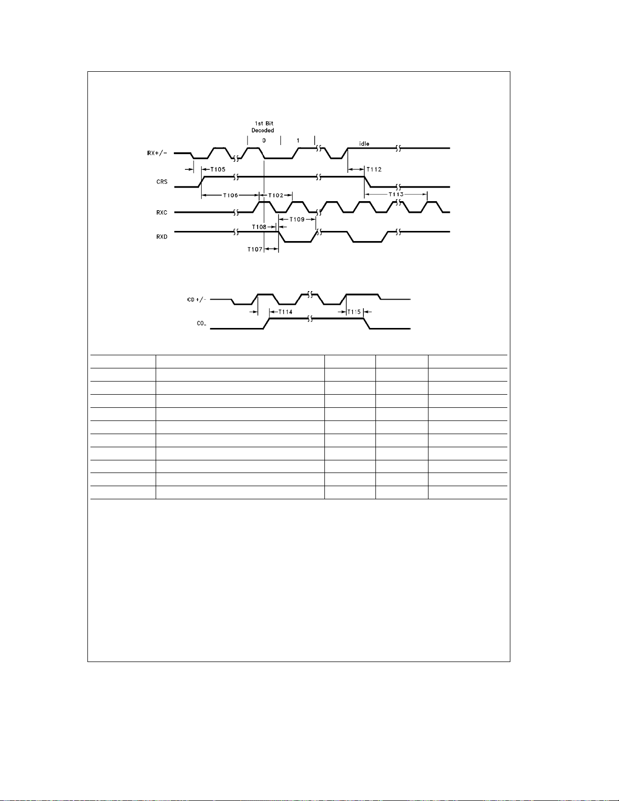
7.0 AC and DC Specifications (Continued)
ENDEC RECEIVE TIMING (INTERNAL ENDEC MODE)
ENDEC COLLISION TIMING
TL/F/11722– 79
Number Parameter Min Max Units
T102 Receive Clock Duty Cycle Time (Note 1) 40 60 ns
T105 Carrier Sense on Time 70 ns
T106 Data Acquisition Time 700 ns
T107 Receive Data Output Delay 150 ns
T108 Receive Data Valid from RXC 10 ns
T109 Receive Data Stable Valid Time 90 ns
T112 Carrier Sense Off Delay (Note 2) 155 ns
T113 Minimum Number of RXCs after CRS Low 5 rcyc (Note 3)
T114 Collision Turn On Time 55 ns
T115 Collision Turn Off Time 250 ns
Note 1: This parameter is measured at the 50% point of each clock edge.
Note 2: When CRSi goes low, it remains low for a minimum of 2 receive clocks (RXCs).
Note 3: rcyc
e
receive clocks.
TL/F/11722– 78
91
Page 92
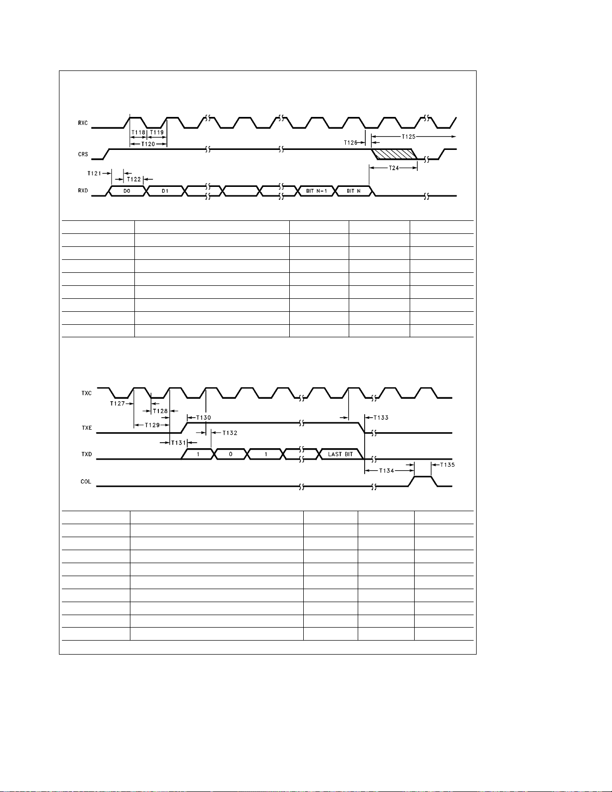
7.0 AC and DC Specifications (Continued)
ENDEC-MAC SERIAL TIMING FOR RECEPTION (EXTERNAL ENDEC MODE)
TL/F/11722– 80
Number Parameter Min Max Units
T118 Receive Clock High Time 35 ns
T119 Receive Clock Low Time 35 ns
T120 Receive Clock Cycle Time 90 110 ns
T121 RXD Setup to RXC 20 ns
T122 RXD Hold from RXC 15 ns
T124 Maximum Allowed Dribble Bits 6 Bits
T125 Receive Recovery Time (Note 2)
T126 RXC to Carrier Sense Low (Note 1) 1 rcyc
Note 1: tcycetransmit clocks, rcycereceive clocks, bcyceT3.
Note 2: This parameter refers to longest time (not including wait-states) the SONIC-16 requires to perform its end of receive processing and be ready for the next
start of frame delimiter. This time is 4 tcyc
ENDEC-MAC SERIAL TIMING FOR TRANSMIT (NO COLLISION)
a
36 bcyc. This is guaranteed by design and is not tested.
Number Parameter Min Max Units
T127 Transmit Clock High Time 40 ns
T128 Transmit Clock Low Time 40 ns
T129 Transmit Clock Cycle Time 90 110 ns
T130 TXC to TXE High 40 ns
T131 TXC to TXD Valid 15 ns
T132 TXD Hold Time from TXC 5 ns
T133 TXC to TXE Low 40 ns
T134 TXE Low to Start of CD Heartbeat (Note 1) 64 tcyc
T135 Collision Detect Width (Note 1) 2 tcyc
Note 1: tcycetransmit clock.
92
TL/F/11722– 81
Page 93

7.0 AC and DC Specifications (Continued)
ENDEC-MAC SERIAL TIMING FOR TRANSMISSION (COLLISION)
Number Parameter Min Max Units
T135 Collision Detect Width (Note 1) 2 tcyc
T136 Delay from Collision 8 tcyc
T137 Jam Period 32 tcyc
Note 1: tcycetransmit clock.
TL/F/11722– 82
93
Page 94

8.0 AC Timing Test Conditions
All specifications are valid only if the mandatory isolation is
employed and all differential signals are taken to be at the
AUI side of the pulse transformer.
Input Pulse Levels (TTL/CMOS) GND to 3.0V
Input Rise and Fall Times (TTL/CMOS) 5 ns
Input and Output Reference
Levels (TTL/CMOS) 1.5V
Input Pulse Levels (Diff.)
Input and Output 50% Point of
Reference Levels (Diff.) the Differential
TRI-STATE Reference Levels Float (DV)
OUTPUT LOAD (See Figure below)
b
350 mV tob1315 mV
g
0.5V
PIN CAPACITANCE
e
T
25§C, fe1 MHz
A
Symbol Parameter Typ Units
C
IN
C
OUT
Input Capacitance 7 pF
Output Capacitance 7 pF
DERATING FACTOR
Output timing is measured with a purely capacitive load of
50 pF. The following correction factor can be used for other
loads: C
t
50 pFa0.05 ns/pF.
L
AUI Transmit Test Load
Note 1: 50 pF, includes scope and jig capacitance.
Note 2: S1
e
Open for timing tests for push pull outputs.
e
S1
VCCfor VOLtest.
e
S1
GND for VOHtest.
e
S1
VCCfor High Impedance to active low and active low to High
Impedance measurements.
e
S1
GND for High Impedance to active high and active High to
High Impedance measurements.
TL/F/11722– 83
Note: In the above diagram, the TXaand TXbsignals are taken from the
AUI side of the isolation (pulse transformer). The pulse transformer
used for all testing is a selected 100 mH
PE64103.
TL/F/11722– 84
g
0.1% Pulse Engineering
94
Page 95

95
Page 96

Physical Dimensions inches (millimeters)
132-Lead Plastic Chip Carrier
DP83916 SONIC-16 Systems-Oriented Network Interface Controller
Order Number DP83932B
NS Package Number V132A
LIFE SUPPORT POLICY
NATIONAL’S PRODUCTS ARE NOT AUTHORIZED FOR USE AS CRITICAL COMPONENTS IN LIFE SUPPORT
DEVICES OR SYSTEMS WITHOUT THE EXPRESS WRITTEN APPROVAL OF THE PRESIDENT OF NATIONAL
SEMICONDUCTOR CORPORATION. As used herein:
1. Life support devices or systems are devices or 2. A critical component is any component of a life
systems which, (a) are intended for surgical implant support device or system whose failure to perform can
into the body, or (b) support or sustain life, and whose be reasonably expected to cause the failure of the life
failure to perform, when properly used in accordance support device or system, or to affect its safety or
with instructions for use provided in the labeling, can effectiveness.
be reasonably expected to result in a significant injury
to the user.
National Semiconductor National Semiconductor National Semiconductor National Semiconductor
Corporation Europe Hong Kong Ltd. Japan Ltd.
1111 West Bardin Road Fax: (
Arlington, TX 76017 Email: cnjwge@tevm2.nsc.com Ocean Centre, 5 Canton Rd. Fax: 81-043-299-2408
Tel: 1(800) 272-9959 Deutsch Tel: (
Fax: 1(800) 737-7018 English Tel: (
National does not assume any responsibility for use of any circuitry described, no circuit patent licenses are implied and National reserves the right at any time without notice to change said circuitry and specifications.
Fran3ais Tel: (
Italiano Tel: (
a
49) 0-180-530 85 86 13th Floor, Straight Block, Tel: 81-043-299-2309
a
49) 0-180-530 85 85 Tsimshatsui, Kowloon
a
49) 0-180-532 78 32 Hong Kong
a
49) 0-180-532 93 58 Tel: (852) 2737-1600
a
49) 0-180-534 16 80 Fax: (852) 2736-9960
 Loading...