

Page 1
查询DP83910A供应商
DP83910A CMOS SNI
Serial Network Interface
General Description
The DP83910A CMOS Serial Network Interface (SNI) is a
direct-pin equivalent of the bipolar DP8391 SNI and provides the Manchester data encoding and decoding functions for IEEE 802.3 Ethernet/Thin-Ethernet type local area
networks. The SNI interfaces the DP8390 Network Interface
Controller (NIC) to the DP8392 CTI or an Ethernet transceiver cable. When transmitting, the SNI converts non-return-tozero (NRZ) data from the controller into Manchester data
and sends the converted data differentially to the transceiver. Conversely, when receiving, a Phase Lock Loop decodes the 10 Mbit/s data from the transceiver into NRZ
data for the controller.
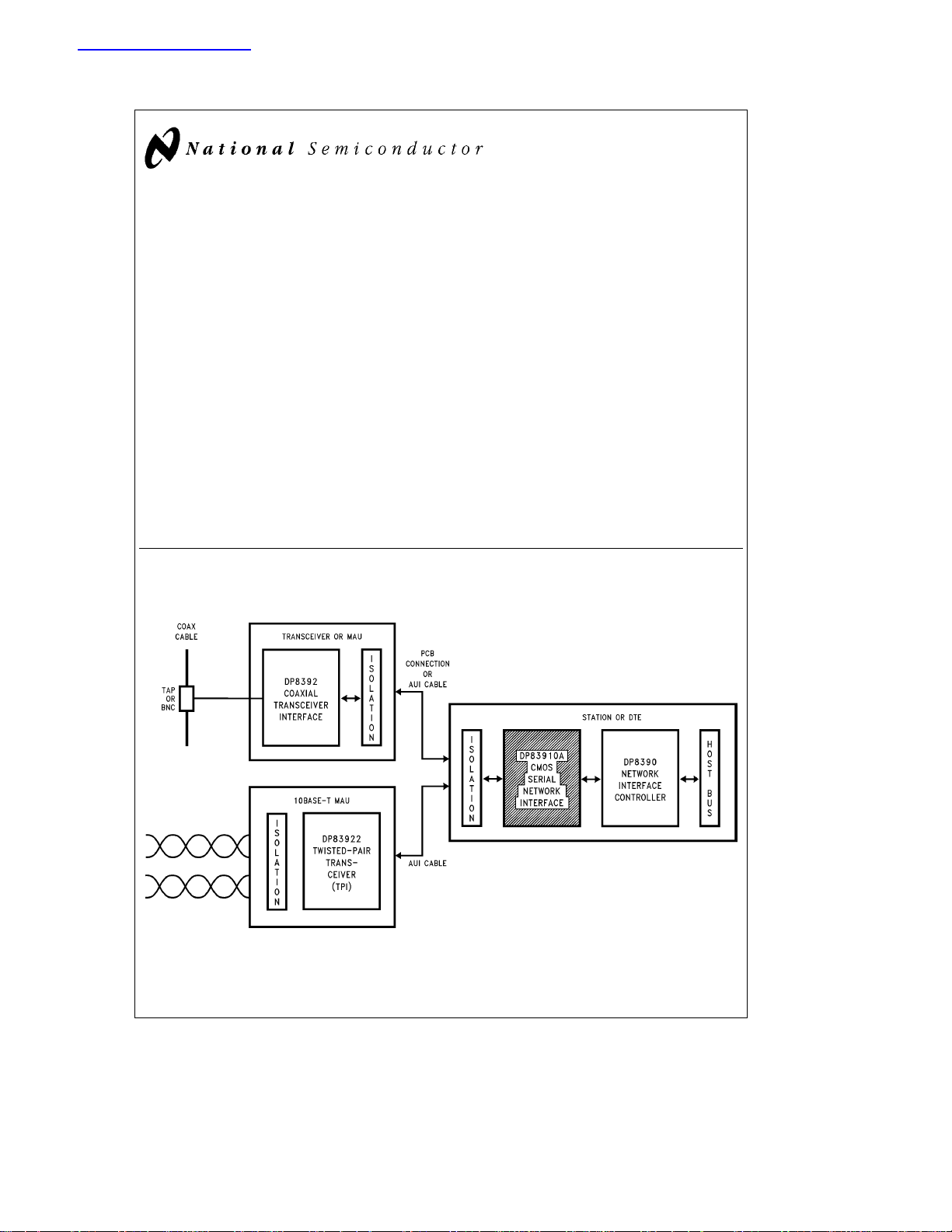
The DP83910A operates in conjunction with the DP8392
Coaxial Transceiver Interface (CTI) and the DP8390 Network Interface Controller (NIC) to form a three-chip set that
implements a complete IEEE 802.3 compatible network as
shown below. The DP83910A is a functionally complete
Manchester encoder/decoder including a balanced driver
and receiver, on-board crystal oscillator, collision signal
translator, and a diagnostic loopback feature. The
May 1995
DP83910A, fabricated CMOS, typically consumes less than
70 mA of current. However, as a result of being CMOS, the
DP83910A’s differential signals must be isolated in both
Ethernet and thin wire Ethernet.
Features
Y
Compatible with Ethernet I, IEEE 802.3; 10BASE5,
10BASE2, and 10BASE-T
Y
Designed to interface with 10BASE-T transceivers
Y
Functional and pin-out duplicate of the DP8391
Y
10 Mbits/s Manchester encoding/decoding with receive
clock recovery
Y
Requires no precision components
Y
Loopback capability for diagnostics
Y
Externally selectable half or full step modes of operation at transmit output
Y
Squelch circuitry at the receive and collision inputs to
reject noise
Y
TTL/MOS compatible controller interface
DP83910A CMOS SNI Serial Network Interface
1.0 System Diagram
IEEE 802.3 Compatible Ethernet/Thin-Ethernet/10 BaseT
TRI-STATEÉis a registered trademark of National Semiconductor Corporation.
C
1995 National Semiconductor Corporation RRD-B30M105/Printed in U. S. A.
TL/F/9365
Local Area Network Chip Set
TL/F/9365– 1
Page 2
2.0 Block Diagram
3.0 Functional Description
The DP83910A consists of five main logical blocks:
a) The oscillator generates the 10 MHz transmit clock signal
for system timing.
b) The Manchester encoder accepts NRZ data from the
controller, encodes the data to Manchester, and transmits it differentially to the transceiver, through the differential transmit driver.
c) The Manchester decoder receives Manchester data from
the transceiver, converts it to NRZ data and clock pulses,
and sends it to the controller.
d) The collision translator indicates to the controller the
presence of a valid 10 MHz collision signal to the PLL.
e) The loopback circuitry, when asserted, routes the data
from the Manchester encoder back to the PLL decoder.
3.1 OSCILLATOR
The oscillator is controlled by a 20 MHz parallel resonant
crystal connected between X1 and X2 or by an external
clock on X1. The 20 MHz output of the oscillator is divided
by 2 to generate the 10 MHz transmit clock for the controller. The oscillator also provides internal clock signals to the
encoding and decoding circuits.
If a crystal is connected to the DP83910A, it is recommended that the circuit shown in
components used meet the following:
Crystal XT1: AT cut parallel resonant crystal
Series Resistance:
Specified Load Capacitance: 13.5 pF
Accuracy: 0.005% (50 ppm)
C1, C2: Load Capacitor, 27 pF.
The resistor, R1, in
minimize frequency drift due to changes in the V
voltage. If R1 is required, it’s value must be carefully selected. R1 decreases the loop gain. Thus, if R1 is made too
large, the loop gain will be greatly reduced and the crystal
will not oscillate. If R1 is made too small, normal variations
in the V
specification. As the first rule of thumb, the value of R1
may cause the oscillation frequency to drift out of
CC
s
10X
Figure 1
Figure 1
be used and that the
may be required in order to
CC
supply
TL/F/9365– 2
Note 1: The resistor R1 may be required in order to minimize frequency drift
due to changes in the V
FIGURE 1. Crystal Connection to DP83910A
. See text description.
CC
TL/F/9365– 15
(see text for component values)
should be made equal to five times the motional resistance
of the crystal.
The motional resistance of 20 MHz crystals is usually in the
range of 10X to 30X. This implies that a reasonable value
for R1 should be in the range of 50X – 150X.
The decision of whether or not to include R1 should be
based upon measured variations of crystal frequency as
each of the circuit parameters is varied.
According to the IEEE 802.3 standard, the entire oscillator
circuit (crytsal and amplifier) must be accurate to 0.01%.
When using a crystal, the X1 pin is not guaranteed to provide a TTL compatible logic output, and should not be used
to drive external standard logic. If additional logic needs to
be driven, then an external oscillator should be used, as
described in the following.
3.2 OSCILLATOR MODULE OPERATION
If the designer wishes to use a crystal clock oscillator, one
that provides the following should be employed:
1) TTL or CMOS output with a 0.01% frequency tolerance
2) 40% – 60% duty cycle
t
3)
2 TTL load output drive (I
e
3.2 mA)
OL
2
Page 3
3.0 Functional Description (Continued)
Figure 2
The circuit is shown in
be necessary if the oscillator must also drive other components.) When using a clock oscillator it is still recommended
that the designer connect the oscillator output to the X1 pin
and tie the X2 pin to ground.
3.3 MANCHESTER ENCODER AND
DIFFERENTIAL DRIVER
The encoder begins operation when the Transmit Enable
input (TXE) goes high and converts clock and NRZ data to
Manchester data for the transceiver. For the duration of
TXE remaining high, the Transmitted Data (TXD) is encoded
for the transmit-driver pair (TX
rising edge of Transmit Clock (TXC). Transmission ends
when TXE goes low. The last transition is always positive; it
occurs at the center of the bit cell if the last bit is a one, or at
the end of the bit cell if the last bit is a zero.
The differential transmit pair from the secondary of the isolation transformer drives up to 50 meters of twisted pair AUI
cable. These outputs are source followers which require two
270X pull-down resistors to ground.
The DP83910A allows both half-step and full-step to be
compatible with Ethernet I and IEEE 802.3. With the SEL pin
low (for Ethernet I), transmit
b
transmit
transmit
during idle; with SEL high (for IEEE 802.3),
a
and transmitbare equal in the idle state. This
provides zero differential voltage to operate with transformer coupled loads.
FIGURE 2. DP83910A Connection for Oscillator Module
. (Additional output drive may
g
). TXD must be valid on the
a
is positive with respect to
TL/F/9365– 16
3.4 MANCHESTER DECODER
The decoder consists of a differential receiver and a PLL to
separate Manchester encoded data stream into clock signals and NRZ data. The differential input must be externally
terminated with two 39X resistors connected in series if the
standard 78X transceiver drop cable is used; in Thin-Ethernet applications, these resistors are optional. To prevent
noise from falsely triggering the decoder, a squelch circuit at
the input rejects signals with levels less than
b
175 mV.
Once the input exceeds the squelch requirements, Carrier
Sense (CRS) is asserted. Receive data (RXD) and receive
clock (RXC) become valid typically within 6 bit times. The
DP83910A may tolerate bit jitter up to 18 ns in the received
data.
The decoder detects the end of a frame when no more
midbit transitions are detected. Within one and a half bit
times after the last bit, carrier sense is de-asserted. Receive
clock stays active for five more bit times after CRS goes low
to guarantee the receive timings of the DP8390 NIC.
3.5 COLLISION TRANSLATOR
When the Ethernet transceiver (DP8392 CTI) detects a collision, it generates a 10 MHz signal to the differential collision
inputs (CD
g
) of the DP83910A. When these inputs are detected active, the DP83910A translates the 10 MHz signal
to an active high level for the controller. The controller uses
this signal to back off its current transmission and reschedule another one.
The collision differential inputs are terminated the same way
as the differential receive inputs. The squelch circuitry is
also similar, rejecting pulses with levels less than
b
175 mV.
3.6 LOOPBACK FUNCTIONS
When the Loopback input (LBK) is asserted high, the
DP83910A redirects its transmitted data back into its receive path. This feature provides a convenient method for
testing both chip and system level integrity. The transmit
driver and receive input circuitry are disabled in loopback
mode.
4.0 Connection Diagrams
Top View
Order Number DP83910AV
See NS Package Number V28A
TL/F/9365– 17
Top View
TL/F/9365– 18
Order Number DP83910AN
See NS Package Number N24C
3
Page 4
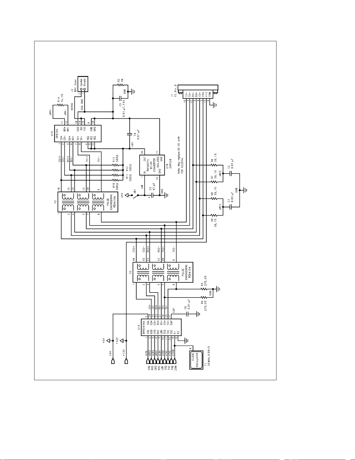
5.0 Typical Application
TL/F/9365– 3
Interface for Ethernet and Thin Wire Ethernet Using Single Jumper for Thin/Thick Selection
4
Page 5

6.0 Pin Descriptions
24-Pin DIP 28-Pin PCC Name I/O Description
1 1 COL O COLLISION DETECT OUTPUT: Generates an active high signal when
2 2 RXD O RECEIVE DATA OUTPUT: NRZ data output from the PLL. This signal
3 3 CRS O CARRIER SENSE: Asserted on the first valid high-to-low transition on
4 4 RXC O RECEIVE CLOCK: The receive clock from the Manchester data after
5 5 SEL I MODE SELECT: When high, transmitaand transmitbare the same
67VSSGROUND PIN
8V
9V
SS
SS
7 10 LBK I LOOPBACK: When high, the loopback mode is enabled.
811X1ICRYSTAL OR EXTERNAL OSCILLATOR INPUT
912X2OCRYSTAL FEEDBACK OUTPUT: Used in crystal connections only.
10 13 TXD I TRANSMIT DATA INPUT: NRZ data input from the controller. The
11 14 TXC O TRANSMIT CLOCK: The 10 MHz clock derived from the 20 MHz
12 15 TXE I TRANSMIT ENABLE: The encoder begins operation when this input is
13 16 TX
14 17 TX
b
a
15 6 NC NO CONNECTION: This may be tied to VSSfor the PLCC version to be
16 18 NC NO CONNECTION
17 19 TEST I FACTORY TEST INPUT: Used to check the chip’s internal functions.
18 20 V
19 21 V
22 V
23 V
DD
DD
DD
DD
20 24 NC NO CONNECTION
21 25 RX
22 26 RX
23 27 CD
24 28 CD
b
a
b
a
10 MHz collision signal is detected.
must be sampled on the rising edge of receive clock.
the RXgpair. Remains active until 1.5 bit times after the last bit in
data.
the PLL has locked. Remains active 5 bit times after deasserting CRS.
voltage in the idle state. When low, transmit
to transmit
b
in the idle state, at the transformer’s primary.
a
is positive with respect
Connected to ground when using an external oscillator.
data is combined with the transmit clock to produce Manchester data.
TXD is sampled on the rising edge of transmit clock.
oscillator.
asserted high.
O TRANSMIT OUTPUT: Differential line driver which sends the encoded
data to the transceiver. The outputs are source followers which require
270X pull-down resistors.
compatible with the DP8391.
May be tied low or have a 0.01 mf bypass capacitor to ground (for
compatibility with the bipolar DP8391) during normal operation.
POWER CONNECTION
I RECEIVE INPUT: Differential receive input pair from the transceiver.
I COLLISION INPUT: Differential collision pair input from the
transceiver.
5
Page 6

7.0 Absolute Maximum Ratings
If Military/Aerospace specified devices are required,
please contact the National Semiconductor Sales
Office/Distributors for availability and specifications.
Supply Voltage (V
CC
)
DC Input Voltage (VIN)
DC Output Voltage (V
OUT
)
Differential Input Voltage
Differential Output Voltage 0 to 16V
Power Dissipation 500 mW
Storage Temperature
b
0.5V toa7V
b
0.5V to V
b
0.5V to V
b
b
65§Ctoa150§C
a
0.5V
CC
a
0.5V
CC
5.5 toa16V
Lead Temperature (Soldering, 10 sec.) 260
ESD (R
Note:
e
1.5 kX,C
ZAP
Absolute maximum ratings are those values beyond
ZAP
e
120 pF)
(Pin 4
e
t
2kV
1.5 kV)
which the safety of the device cannot be guaranteed. They
are not meant to imply that the device should be operated at
these limits.
*Note: An asterisk following a parameter’s symbol indicates that the param-
eter has been characterized but not tested.
Note: All specifications in this datasheet are valid only if the mandatory
isolation is employed and all differential signals are taken to exist at the AUI
side of the pulse transformer.
C
§
8.0 DC Specifications T
e
0§Cto70§C, V
A
CC
e
5Vg5%
Symbol Parameter Conditions Min Typ Max Units
Controller Interface Pins (COL, RXD, CRS, RXC, SEL, LBK, TXD, TXC and TXE)
V
V
I
IN
V
V
I
CCO
I
CCS
IH
IL
OH
OL
Input High Voltage 2.0 V
Input Low Voltage 0.8 V
Input Leakage V
IN
Output High Voltage (TTL) I
(CMOS) I
Output Low Voltage (TTL) I
(CMOS) I
Operating VCCSupply
Current (Note 1)
Stand By VCCSupply
Current (Note 2)
10 Mbit/sec 70 mA
10 Mbit/sec 65 mA
e
VCCor GND
e
2.0 mA 3.5 V
OH
e
20 mAV
OH
e
2.0 mA 0.4 V
OL
e
20 mA 0.1 V
OL
b
1.0 1.0 mA
b
0.1 V
CC
Differential Pins (TXg,RXg, and CDg)
V
OD
VOB* Diff. Output Voltage 78X Termination, and
VU* Undershoot Voltage (TXg)78XTermination, and
V
DS
V
CM
Diff. Output Voltage (TXg)78XTermination, and
270X from each to GND
Imbalance (TX
g
) 270X from each to GND
270X from each to GND
Diff. Squelch Threshold
g
and CDg)
(RX
Diff. Input Common Mode
Voltage (RX
g
and CDg) 0 5.5 V
(Figure 4)
(Figure 4)
(Figure 4)
g
550
g
1200 mV
40 mV
100 mV
b
175
b
300 mV
(Note 3)
Oscillator Pins (X1 and X2)
V
IH
V
IL
I
OSC
Note 1: This measurement was made while the DP83910A was undergoing transmission, reception, and collision detection. Also, this value was not measured
instantaneously, but averaged over a span of several milliseconds. (V
Note 2: This measurement was made while the DP83910A was sitting idle with TXE low. Also, this value was not measured instantaneously, but averaged over a
span of several milliseconds. (V
Note 3: This parameter is guaranteed by design and is not tested.
X1 Input High Voltage X1 is connected to an oscillator,
and X2 is grounded
X1 Input Low Voltage X1 is connected to an oscillator,
and X2 is grounded
X1 Input Current X1eVCCor GND
e
GND
X2
e
2.4V or 0.4V and I
e
2.4V or 0.4V and I
IN
IN
e
0 mA).
o
o
e
0 mA).
2.0 V
0.8 V
b
2
a
2mA
6
Page 7

9.0 Switching Characteristics T
e
0§Cto70§C, V
A
CC
e
5Vg5%
Oscillator Specification
Symbol Parameter Min Max Units
t
t
XTH
XTL
X1 to Transmit Clock High 5 30 ns
X1 to Transmit Clock Low 5 30 ns
Transmit Timing (Start of Packet)
TL/F/9365– 4
Transmit Specifications (Start of Packet)
Symbol Parameter Min Max Units
t
TCh
t
TCl
t
* Transmit Clock Cycle Time (Note 1) 99.99 100.01 ns
TCc
t
* Transmit Clock Rise Time (20% to 80%) (C
TCr
t
* Transmit Clock Fall Time (80% to 20%) (C
TCf
t
TEs
t
TDs
t
TDh
t
TOd
t
* Transmit Output Fall Time (80% to 20%) 7 ns
TOf
t
* Transmit Output Rise Time (20% to 80%) 7 ns
TOr
t
* Transmit Output Jitter 0.5 Typical ns
TOj
Note 1: This parameter is measured using the fifty percent point of each clock edge.
Transmit Clock High Time (Note 1) 40 60 ns
Transmit Clock Low Time (Note 1) 40 60 ns
e
30 pF) 8 ns
L
e
30 pF) 8 ns
L
Transmit Enable Setup Time to Rising Edge of TXC (Note 1) 20 ns
Transmit Data Setup Time from Rising Edge of TXC (Note 1) 20 ns
Transmit Data Hold Time
from Rising Edge of TXC
0ns
Transmit Output Delay from Rising Edge of TXC (Note 1) 65 ns
7
Page 8

9.0 Switching Characteristics (Continued)
Transmit Timing (End of Packet)
TL/F/9365– 5
Transmit Specifications (End of Packet)
Symbol Parameter Min Max Units
t
TXEh
t
TOh
t
* Transmit Output Idle Time (Half Step) 8000 ns
TOi
Transmit Enable Hold Time from Rising Edge of TXC 0 ns
Transmit Output High before Idle (Half Step) 200 ns
Receive Timing (Start of Packet)
TL/F/9365– 6
Receiver Specifications (Start of Packet)
Symbol Parameter Min Max Units
t
RCd
t
* Receive Clock Rise Time (20% to 80%, C
RCr
t
* Receive Clock Fall Time (80% to 20%, C
RCf
t
CRSon
t
DAT
t
RDd
t
RDs
t
Dtor
t
RDV
Note 1: This parameter is measured using the fifty percent point of each clock edge.
Note 2: This parameter was characterized with a differential input of
Receive Clock Duty Cycle (Note 1) 40 60 %
e
30 pF) 7 ns
TL
e
30 pF) 7 ns
TL
Carrier Sense Turn On Delay 70 ns
Decoder Acquisition Time 700 ns
Receive Data Output Delay 150 ns
Receive Data Output Stable after Going Valid 90 ns
Differential Inputs Turn-On Pulse (Note 2) 30 ns
Receive Data Output Valid from Falling Edge of RXC 10 ns
b
375 mV on the receive pair inputs.
8
Page 9

9.0 Switching Characteristics (Continued)
Receive Timing (End of Packet)
TL/F/9365– 7
Receiver Specifications (End of Packet)
Symbol Parameter Min Max Units
t
CRSoff
t
RXCh
Note 1: When CRS goes low, it will go low a minimum of 2 receive clocks.
Note 2: The DP8390 Network Interface Controller (NIC) requires a minimum of 5 receive clocks after CRS goes low to function properly.
Carrier Sense Turn Off Delay (Note 1) 155 ns
Minimum Number of RXCs after CRS Low (Note 2) 5 Bit Times
Collision Timing
TL/F/9365– 8
Collision Specifications
Symbol Parameter Min Max Units
t
COLon
t
COLoff
t
Dtoc
Note 1: This parameter was characterized with a differential input ofb375 mV on the collision input pair.
Collision Turn On Delay 60 ns
Collision Turn Off Delay 350 ns
Differential Inputs Turn-On
Pulse (Squelch, Note 1)
30 ns
9
Page 10

9.0 Switching Characteristics (Continued)
Loopback Timing
TL/F/9365– 9
Loopback Specifications
Symbol Parameter Min Max Units
t
LBs
t
LBh
Note 1: This parameter is guaranteed by design and is not tested.
Loopback Setup Time (Note 1) 50 ns
Loopback Hold Time (Note 1) 1000 ns
AC Timing Test Conditions
All specifications are valid only if the mandatory isolation is
employed and all differential signals are taken to be at the
AUI side of the pulse tranformer.
Input Pulse Levels (TTL/CMOS) GND to 3.0V
Input Rise and Fall Times (TTL/CMOS) 5 ns
Input and Output Reference Levels
(TTL/CMOS) 1.3V
Input Pulse Levels
(Diff.)
Input and Output 50% Point of
Reference Levels (Diff.) the Differential
FIGURE 3
b
350 tob1315 mV
TL/F/9365– 10
Capacitance T
e
25§C, fe1 MHz
A
Symbol Parameter Typ Units
C
C
IN
OUT
Input Capacitance 7 pF
Output Capacitance 7 pF
TL/F/9365– 12
FIGURE 4
Note: In the above diagram, the TXaand TXbsignals are taken from the
AUI side of the isolation (pulse transformer). The pulse transformer used for
all testing is the Pulse Engineering PE64103.
10
Page 11

Physical Dimensions inches (millimeters)
Molded Dual-In-Line Package (N)
Order Number DP83910AN
NS Package Number N24C
11
Page 12

Physical Dimensions inches (millimeters) (Continued)
DP83910A CMOS SNI Serial Network Interface
Plastic Chip Carrier (V)
Order Number DP83910AV
NS Package Number V28A
LIFE SUPPORT POLICY
NATIONAL’S PRODUCTS ARE NOT AUTHORIZED FOR USE AS CRITICAL COMPONENTS IN LIFE SUPPORT
DEVICES OR SYSTEMS WITHOUT THE EXPRESS WRITTEN APPROVAL OF THE PRESIDENT OF NATIONAL
SEMICONDUCTOR CORPORATION. As used herein:
1. Life support devices or systems are devices or 2. A critical component is any component of a life
systems which, (a) are intended for surgical implant support device or system whose failure to perform can
into the body, or (b) support or sustain life, and whose be reasonably expected to cause the failure of the life
failure to perform, when properly used in accordance support device or system, or to affect its safety or
with instructions for use provided in the labeling, can effectiveness.
be reasonably expected to result in a significant injury
to the user.
National Semiconductor National Semiconductor National Semiconductor National Semiconductor
Corporation Europe Hong Kong Ltd. Japan Ltd.
1111 West Bardin Road Fax: (
Arlington, TX 76017 Email: cnjwge@tevm2.nsc.com Ocean Centre, 5 Canton Rd. Fax: 81-043-299-2408
Tel: 1(800) 272-9959 Deutsch Tel: (
Fax: 1(800) 737-7018 English Tel: (
National does not assume any responsibility for use of any circuitry described, no circuit patent licenses are implied and National reserves the right at any time without notice to change said circuitry and specifications.
Fran3ais Tel: (
Italiano Tel: (
a
49) 0-180-530 85 86 13th Floor, Straight Block, Tel: 81-043-299-2309
a
49) 0-180-530 85 85 Tsimshatsui, Kowloon
a
49) 0-180-532 78 32 Hong Kong
a
49) 0-180-532 93 58 Tel: (852) 2737-1600
a
49) 0-180-534 16 80 Fax: (852) 2736-9960
 Loading...