

DP83865 Gig PHYTER® V
10/100/1000 Ethernet Physical Layer
General Description
The DP83865 is a fully featured Physical Layer transceiver
with integrated PMD sublayers to support 10BASE-T,
100BASE-TX and 1000BASE-T Ethernet protocols.
The DP83865 is an ul tra low po wer v ersion of t he DP8 3861
and DP83891. It uses advanced 0.18 um, 1.8 V CMOS
technology, fabricated at National Semiconductor’s South
Portland, Maine facility.
The DP83865 is designed for easy implementation of
10/100/1000 Mb/s Ethernet LANs. It interfaces directly to
Tw isted Pai r media vi a an externa l transfo rmer. This devic e
interfaces directly to the MAC layer through the IEEE
802.3u Standard Media Independent Interface (MII), the
IEEE 802.3z Gigabit Media Independent Interface (GMII),
or Reduced GMII (RGMII).
The DP83865 is a fourth generation Gigabit PHY with field
proven architecture and performance. Its robust performance ensures drop-in replacement of existing
10/100 Mbps equipmen t wi th t en to o ne hundr ed time s t he
performance using the existing networking infrastructure.
Applications
The DP83865 fits applications in:
■ 10/100/1000 Mb/s capable node cards
■ Switches with 10/100/1000 Mb/s capable ports
■ High speed uplink ports (backbone)
Features
■ Ultra low power consumption typically 1.1 watt
■ Fully compliant with IEEE 802.3 10BASE-T, 100BASE-
TX and 1000BASE-T specifications
■ Integrated PMD sub layer featuring adaptive e qualization
and baseline wander compensation according to ANSI
X3.T12
■ 3.3 V or 2.5 V MAC interfaces:
■ IEEE 802.3u MII
■ IEEE 802.3z GMII
■ RGMII version 1.3
■ User progr ammable GMII pin ordering
■ IEEE 802.3u Auto-Negotiation and Parallel Detection
■ Fully Auto-Negotiates between 1000 Mb/s, 100 Mb/s,
and 10 Mb/s full duplex and half duplex devices
■ Speed Fallback mode to achieve quality link
■ Cable length estimator
■ LED support for activity, full / half duplex, link1000,
link100 and link10, user programmable (manual on/off),
or reduced LED mode
■ Supports 25 MHz operation with crystal or oscillator.
■ Requires only two power supplies, 1.8 V (core and
analog) and 2.5 V (analog and I/O). 3.3V is supported
as an alternative supply for I/O voltage
■ User programable interrupt
■ Supports Auto-MDIX at 10, 100 and 1000 Mb/s
■ Supports JTAG (IEEE1 149.1 )
■ 128-pin PQFP package (14mm x 20mm)
DP83865 Gig PHYTER® V 10/100/1000 Ethernet Physical Layer
October 2004
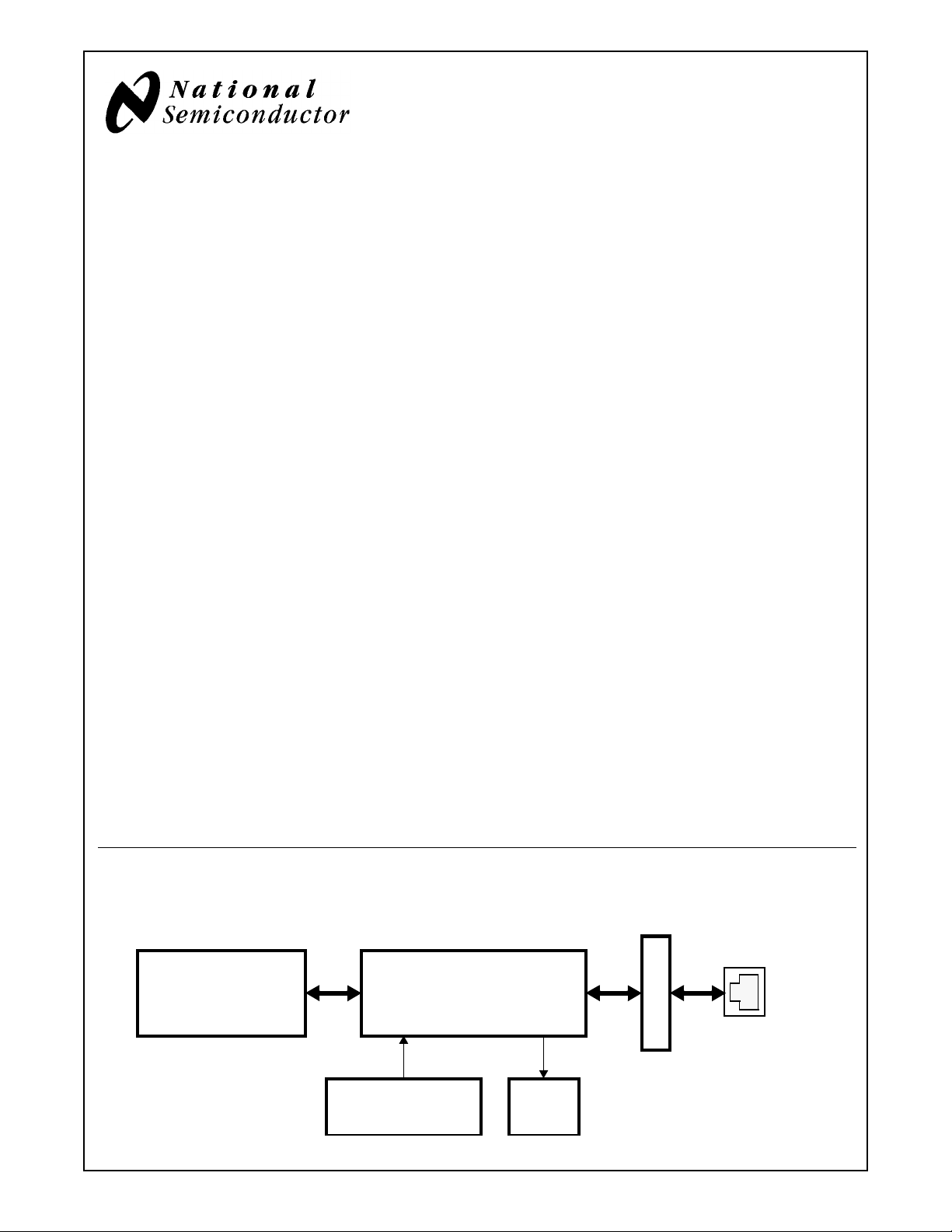
SYSTEM DIAGRAM
MII
GMII
RGMII
10BASE-T
100BASE-TX
1000BASE-T
DP83820
10/100/1000 Mb/s
ETHERNET MAC
PHYTER® is a registered trademark of National Semiconductor Corporation
© 2004 National Semiconductor Corporation www.national.com
ETHERNET PHYSICAL LAYER
25 MHz
crystal or oscillator
DP83865
10/100/1000 Mb/s
STATUS
RJ-45
MAGNETICS
LEDs
Block Diagram
DP83865
MGMT INTERFACE
MDIO
MDC
Interrupt
COMBINED MII / GMII / RGMII INTERFACE
µC MGMT
& PHY CNTRL
100BASE-TX
10BASE-T
Block Block Block
MII
100BASE-TX
PCS
100BASE-TX
PMA
MII
10BASE-T
PLS
10BASE-T
PMA
GTX_CLK
TX_EN
TXD[7:0]
TX_ER
1000BASE-T
1000BASE-T
PCS
1000BASE-T
PMA
TX_CLK
RX_CLK
COL
CRS
RX_ER
MUX/DMUX
GMIIMII
GMII
RX_DV
RXD[7:0]
Echo cancellation
Crosstalk cancellation
ADC
Decode/Descramble
Equalization
Timing
Skew compensation
BLW
100BASE-TX
PMD
MLT-3
100 Mb/s
Manchester
10 Mb/s
PAM-5
17 Level PR Shaped
125 Msymbols/s
DAC/ADC
SUBSYSTEM
TIMING
DRIVERS/
RECEIVERS
DAC/ADC
TIMING BLOCK
MAGNETICS
4-pair CAT-5 Cable
www.national.com 2

Table of Contents
1.0 Pin Description . . . . . . . . . . . . . . . . . . . . . . . . . . . . . . . .5
1.1 MAC Interfaces (MII, GMII, and RGMII) . . . . . . .5
1.2 Management Interface . . . . . . . . . . . . . . . . . . . .7
1.3 Media Dependent Interface . . . . . . . . . . . . . . . .7
1.4 JTAG In te r f a c e . . . . . . . . . . . . . . . . . . . . . . . . . .7
1.5 Clock In terface . . . . . . . . . . . . . . . . . . . . . . . . . .8
1.6 Device Configuration and LED Interface . . . . . . . .8
1.7 Reset . . . . . . . . . . . . . . . . . . . . . . . . . . . . . . . . 10
1.8 Power and Ground Pins . . . . . . . . . . . . . . . . . . . .11
1.9 Special Connect Pins . . . . . . . . . . . . . . . . . . . .11
1.10 Pin Assignments in the Pin Number Order . . . .12
2.0 Regis t e r B lo c k . . . . . . . . . . . . . . . . . . . . . . . . . . . . . . . 18
2.1 Register Definitions . . . . . . . . . . . . . . . . . . . . . . .18
2.2 Regis te r M a p . . . . . . . . . . . . . . . . . . . . . . . . . . 19
2.3 Register Description . . . . . . . . . . . . . . . . . . . . . .21
3.0 Confi guration . . . . . . . . . . . . . . . . . . . . . . . . . . . . . . . .40
3.1 Accessing Expanded Memory Space . . . . . . . . .40
3.2 Manual Configuration . . . . . . . . . . . . . . . . . . . . . .40
3.3 Auto-Negotiation . . . . . . . . . . . . . . . . . . . . . . . . .41
3.4 Auto-Negotiation Register Set . . . . . . . . . . . . . . .44
3.5 Auto-MDIX resolution . . . . . . . . . . . . . . . . . . . . . .44
3.6 Polari ty C o r rection . . . . . . . . . . . . . . . . . . . . . . . .45
3.7 PHY Address, Strapping Options and LEDs . . . . 45
3.8 Reduced LED Mode . . . . . . . . . . . . . . . . . . . . . .45
3.9 Modulate LED on Error . . . . . . . . . . . . . . . . . . . .45
3.10 MAC In t e r f a c e . . . . . . . . . . . . . . . . . . . . . . . . . . . 45
3.11 Clock to MAC Enable . . . . . . . . . . . . . . . . . . . . . .46
3.12 MII/GMII/RGMII Isolate Mode . . . . . . . . . . . . . . .46
3.13 Loopback Mode . . . . . . . . . . . . . . . . . . . . . . . . . .46
3.14 IEEE 802.3ab Test Modes . . . . . . . . . . . . . . . . . .46
3.15 Interrupt . . . . . . . . . . . . . . . . . . . . . . . . . . . . . . . . 47
3.16 Low Power Mode / WOL . . . . . . . . . . . . . . . . . . .47
3.17 Power Down Mode . . . . . . . . . . . . . . . . . . . . . . .47
3.18 BIST Configuration . . . . . . . . . . . . . . . . . . . . . . .47
3.19 Cable Length Indicator . . . . . . . . . . . . . . . . . . . . .48
3.20 10BASE-T Half Duplex Loopback . . . . . . . . . . . .48
3.21 I/O Voltage Selection . . . . . . . . . . . . . . . . . . . . . .48
3.22 Non-compliant inter-operability mode . . . . . . . . .48
4.0 Functional Description . . . . . . . . . . . . . . . . . . . . . . . . .49
4.1 1000BASE-T PCS Transmitter . . . . . . . . . . . . . .49
4.2 1000BASE-T PMA Transmitter . . . . . . . . . . . . . .50
4.3 1000BASE-T PMA Receiver . . . . . . . . . . . . . . . .50
4.4 1000BASE-T PCS Receiver . . . . . . . . . . . . . . . .51
4.5 Gigabit MII (GMII) . . . . . . . . . . . . . . . . . . . . . . . .52
4.6 Reduced GMII (RGMII) . . . . . . . . . . . . . . . . . . . . 53
4.7 10BASE-T and 100BASE-TX Transmitter . . . . . .54
4.8 10BASE-T and 100BASE-TX Receiver . . . . . . . .57
4.9 Media Independent Interface (MII) . . . . . . . . . . . .60
5.0 Desig n Guide . . . . . . . . . . . . . . . . . . . . . . . . . . . . . . . . 63
5.1 Hardw a re R e s e t . . . . . . . . . . . . . . . . . . . . . . . . . .63
5.2 Clocks . . . . . . . . . . . . . . . . . . . . . . . . . . . . . . . . .6 3
5.3 Power Supply Decoupling . . . . . . . . . . . . . . . . . .64
5.4 Sensitive Supply Pins . . . . . . . . . . . . . . . . . . . . . 64
5.5 PCB Layer Stacking . . . . . . . . . . . . . . . . . . . . . . .64
5.6 Layou t N o t e s on MAC Interfac e . . . . . . . . . . . . . . 66
5.7 Twisted Pair Interf a ce . . . . . . . . . . . . . . . . . . . . .66
5.8 RJ-45 Connections . . . . . . . . . . . . . . . . . . . . . . .67
5.9 LED/Strapping Option . . . . . . . . . . . . . . . . . . . . . 67
5.10 Unused Pins and Reserved Pins . . . . . . . . . . . . .67
5.11 I/O Voltage Considerations . . . . . . . . . . . . . . . . .68
5.12 Power-up Recommendations . . . . . . . . . . . . . . .6 8
5.13 Component Selection . . . . . . . . . . . . . . . . . . . . .68
6.0 Electrical Specific a t ions . . . . . . . . . . . . . . . . . . . . . . . 71
6.1 DC Electrical Specification . . . . . . . . . . . . . . . . . 71
6.2 Reset Timing . . . . . . . . . . . . . . . . . . . . . . . . . . . 73
6.3 Clock Timing . . . . . . . . . . . . . . . . . . . . . . . . . . . 74
6.4 1000 Mb/s Timing . . . . . . . . . . . . . . . . . . . . . . . . 74
6.5 RGMII Timing . . . . . . . . . . . . . . . . . . . . . . . . . . . 76
6.6 100 Mb/s Timing . . . . . . . . . . . . . . . . . . . . . . . . . 77
6.7 10 Mb/s Timing . . . . . . . . . . . . . . . . . . . . . . . . . . 78
6.8 Loopback Timing . . . . . . . . . . . . . . . . . . . . . . . . 79
6.9 Serial Management Interface Timing . . . . . . . . . 80
6.10 Power Consumption . . . . . . . . . . . . . . . . . . . . . . 81
7.0 Frequently Asked Questions . . . . . . . . . . . . . . . . . . . 82
7.1 Do I need to access any MDIO register to start up
the PHY? . . . . . . . . . . . . . . . . . . . . . . . . . . . . . . 82
7.2 I am trying to access the registers through MDIO
and I got invalid data. What should I do? . . . . . 82
7.3 Why can the PHY establish a valid link but can
not transmit or receive data? . . . . . . . . . . . . . . . 82
7.4 What is the difference between TX_CLK,
TX_TCLK, and GTX_CLK? . . . . . . . . . . . . . . . . 82
7.5 What happens to the TX_CLK during 1000 Mbps
operation? Similarly what happens to RXD[4:7]
during 10/100 Mbps operation? . . . . . . . . . . . . . 82
7.6 What happens to the TX_CLK and RX_CLK
during Auto-Negotiation and during idles? . . . . . 82
7.7 Why doesn’t the Gig PHYTER V complete AutoNegotiation if the link partner is a forced
1000 Mbps PHY? . . . . . . . . . . . . . . . . . . . . . . . . 82
7.8 What determines Master/Slave mode when AutoNegotiation is disabled in 1000Base-T mode? . . 82
7.9 How long does Auto-Negotiation take? . . . . . . . 83
7.10 How do I measure FLP’s? . . . . . . . . . . . . . . . . . 83
7.11 I have forced 10 Mbps or 100 Mbps operation but
the associated speed LED doesn’t come on. . . . 83
7.12 I know I have good link, but register 0x01, bit 2
“Link Status” doesn’t contain value ‘1’ indicating
good link. . . . . . . . . . . . . . . . . . . . . . . . . . . . . . . 83
7.13 Your reference design shows pull-up or pull-down
resistors attached to certain pins, which conflict
with the pull-up or pull-down information specified
in the datasheet? . . . . . . . . . . . . . . . . . . . . . . . . 83
7.14 How is the maximum package case temperature
calculated? . . . . . . . . . . . . . . . . . . . . . . . . . . . . . 83
7.15 The DP83865 will establish Link in 100 Mbps
mode with a Broadcom part, but it will not
establish link in 1000 Mbps mode. When this
happens the DP83865’s Link LED will blink on
and off. . . . . . . . . . . . . . . . . . . . . . . . . . . . . . . . . 83
7.16 How do I quickly determine the quality of the
link over the cable ? . . . . . . . . . . . . . . . . . . . . . . 83
7.17 What is the power up sequence for DP83865? . 83
7.18 What are some other applicable documents? . . 84
8.0 Physical Dimensions . . . . . . . . . . . . . . . . . . . . . . . . . 86
3 www.national.com
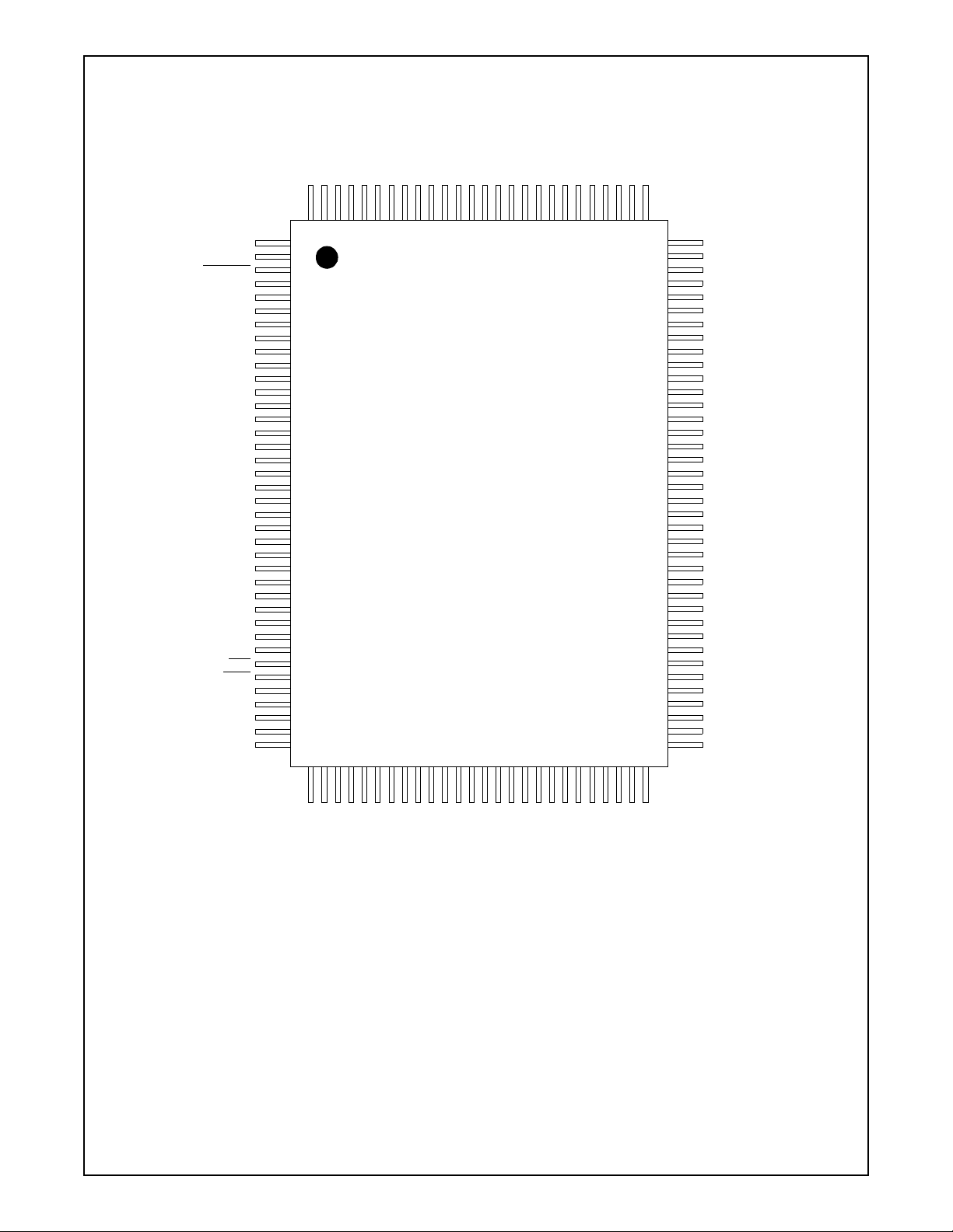
PQFP Pin Layout
DP83865
TX_TCLK / MAN_MDIX_STRA P
ACTIVITY_LED / SPEED0_STRAP
LINK10_LED / RLED/SPEED1_STRAP
LINK100_LED / DUPLEX_STRAP
LINK1000_LED / AN_EN_STRAP
DUPLEX_LED / PHYADDR0_STRAP
NON_IEEE_STRAP
RESERVED
INTERRUPT
IO_VDD
VSS
CORE_VDD
VSS
PHYADDR1_STRAP
IO_VDD
VSS
PHYADDR2_STRAP
PHYADDR3_STRAP
CORE_VDD
VSS
IO_VDD
VSS
RESERVED
TCK
CORE_VDD
VSS
TMS
TDO
IO_VDD
VSS
TDI
TRST
RESET
VDD_SEL_STRAP
CORE_VDD
VSS
IO_VDD
VSS
1V8_AVDD1
VSS
43
124
MDIC_N
VSS
121
122
123
46
45
44
MDID_N
MDID_P
VSS
VSS
125
126
127
128
1
2
3
4
5
6
7
8
9
10
11
12
13
14
15
16
17
18
19
20
21
22
23
24
25
26
27
28
29
30
31
32
33
34
35
36
37
38
42
41
40
39
1V8_AVDD1
MDIC_P
VSS
119
120
MDIB_N
VSS
VSS
115
117
116
118
DP83865DVH
Gig PHYTER V
52
50
48
51
49
47
1V8_AVDD1
MDIA_N
MDIB_P
VSS
VSS
112
113
114
55
54
53
MDIA_P
VSS
VSS
108
110
107
109
111
59
57
60
58
56
1V8_AVDD1
1V8_AVDD1
VSS
VSS
103
106
104
105
102
101
100
99
98
97
96
95
94
93
92
91
90
89
88
87
86
85
84
83
82
81
80
79
78
77
76
75
74
73
72
71
70
69
68
67
66
65
64
61
63
62
BG_REF
2V5_AVDD1
1V8_AVDD3
VSS
1V8_AVDD2
VSS
2V5_AVDD2
PHYADDR4_STRAP
MUL T I_ EN_STRAP / TX_TRIGGER
VSS
CORE_VDD
VSS
IO_VDD
MDIX_EN_STRAP
MAC_CLK_EN_STRAP
CLK_OUT
CLK_IN
CLK_TO_MAC
RESERVED
IO_VDD
VSS
MDC
MDIO
GTX_CLK/TCK
VSS
IO_VDD
TXD0/TX0
TXD1/TX1
VSS
CORE_VDD
TXD2/TX2
TXD3/TX3
VSS
IO_VDD
TXD4
TXD5
TXD6
TXD7
RXD4
CORE_VDD
VSS
RXD5
RXD6
RXD7
RX_DV/RCK
VSS
IO_VDD
RX_ER/RXDV_ER
CRS/RGMII_SEL0
COL/CLK_MAC_FREQ
Figure 1. DP83865 Pinout
Order Part Number: DP83865DVH
www.national.com 4
RXD1/RX1
RXD2/RX2
VSS
RXD3/RX3
IO_VDD
VSS
RX_CLK
TX_CLK/RGMII_SEL1
IO_VDD
RXD0/RX0
VSS
TX_ER
CORE_VDD
TX_EN/TXEN_ER

1.0 Pin Description
The DP83865 pins are c lassifi ed into the fol lowing i nterfac e
categories (each is described in the sections that follow):
— MAC Interfaces
— Management Interface
— Media Dependent Interface
—JTAG Interface
— Clock Interface
— Device Configuration and LED Interfa ce
—Reset
— Power and Ground Pins
— Special Connect Pins
1.1 MAC Interfaces (MII, GMII, and RGMII)
DP83865
Type: I Inputs
Type: O Output
Type: O_Z Tristate Output
Type: I/O_Z Tristate Input_Output
Type: S Strapping Pin
Type: PU Internal Pull-up
Type: PD Internal Pull-down
Signal Name Type
CRS/RGMII_SEL0 O_Z,
S, PD
COL/CLK_MAC_FREQ O_Z,
S, PD
TX_CLK/RGMII_SEL1 O_Z,
S, PD
PQFP
Pin #
40 C ARRIER SENSE or RGMII SELECT: CRS is asserted high to indicate the
presence of a carrier due to receive or transmit activity in Half Duplex mode.
For 10BASE-T and 100BASE-TX Full Duplex operation CRS is as serted when
a received packet is detected. This signal is not defined for 1000BASE-T Full
Duplex mode.
In RGMII mode, the CRS is not used. This pin can be used as a RGMII strapping selection pin.
RGMII_SEL1
00= GMII
01= GMII
1 0 = RGMII - HP
1 1 = RGMII - 3COM
39 COLLISION DETECT: Asserted hig h to indic ate dete ction o f a collis ion co ndi-
tion (assertion of CRS due to simultaneous transmit and receive activity) in
Half Duplex modes. This signal is not synchronous to either MII clock
(GTX_CLK, TX_CLK or RX_CLK). This signal is not defined and stays low for
Full Duplex modes.
CLOCK TO MAC FREQUENCY Select:
1 = CLOCK TO MAC output is 125 MHz
0 = CLOCK TO MAC output is 25 MHz
60 TRANSMIT CLOCK or RGMII SELECT: TX_CLK is a cont inu ous cloc k sig nal
generated from reference CLK_IN and driven by the PHY during 10 Mbps or
100 Mbps MII mode. TX_ CLK clocks the data or error ou t of the MAC layer and
into the PHY.
The TX_CLK clock frequency is 2.5 MHz in 10BASE-T and 25 MHz in
100BASE-TX mode.
Note: “TX_CLK” should not be confused with the “TX_TCLK” signal.
In RGMII mode, the TX_CLK is not used. This pin can be used as a RGMII
strapping selection pin. This pin should be pulled high for RGMII interface.
RGMII_SEL0 MAC Interface
Description
5 www.national.com

1.0 Pin Description (Continued)
DP83865
Signal Name Type
TXD0/TX0
TXD1/TX1
TXD2/TX2
TXD3/TX3
TXD4
TXD5
TXD6
TXD7
TX_EN/TXEN_ER I 62 TRANSMIT ENABLE or TRANSMIT ENABLE/ERROR: In MII or GMII mo de ,
GTX_CLK/TCK I 79 GMII and RGMII TRANSMIT CLOCK: This continu ous cloc k signal i s sourced
TX_ER I 61 TRANSM IT ERROR: It is an active high input used in MII mode and GMII
RX_CLK O_Z 57 RECEIVE CLOCK: Provides the recove red receive clocks for d iffe rent modes
RXD0/RX0
RXD1/RX1
RXD2/RX2
RXD3/RX3
RXD4
RXD5
RXD6
RXD7
RX_ER/RXDV_ER O_Z 41 RECEIVE ERROR or RECEIVE DATA AVAILABLE/ERROR: In 10 Mbps,
RX_DV/RCK O_Z 44 RECEIVE DATA VALID or RECEIVE CLOCK: In MII and GMII modes, it is as-
PQFP
Pin #
I76
75
72
71
68
67
66
65
O_Z 56
55
52
51
50
47
46
45
Description
TRANSMIT DATA: These signals carry 4B data nibbles (TXD[3:0]) during 10
Mbps and 100 Mbps MII mode, 4-bit data (TX[3:0]) in RGMII mode, and 8-bit
data (TXD[7:0]) in 1000 Mbps GMII mode. They are synchronous to the transmit clocks (TX_CLK, TCK, GTX_CLK).
Transmit data is input to PHY. In MII or GMII mode, the transmit data is enabled by TX_EN. In RGMII mode, the transmit data is enabled by TXEN_ER.
it is an active high in pu t s ourc ed fro m M AC l ay er t o i ndi ca te t r ans m issio n d ata
is available on the TXD.
In RGMII mode, it combines the transm it en able and the trans m it error si gna ls
of GMII mode using both clock edges.
from the MAC layer to the PHY. Nominal frequency is 125 MHz.
mode forcing the PHY to transmit invalid symbols. The TX_ER signal is synchronous to the transmit clocks (TX_CLK or GTX_CLK).
In MII 4B nibble mode, assertion of Transmit Error by t he controller cau ses the
PHY to issue invalid symbols foll owed by Halt (H) s ymbols until dea ssertion occurs.
In GMII mode, assertion causes the PHY to emit one or more code-groups that
are invalid data or delimiter in the transmitted frame.
This signal is not used in the RGMII mode.
of operation:
2.5 MHz in 10 Mbps mode.
25 MHz in 100 Mbps mode.
125 MHz in 1000 Mps GMII mode.
This pin is not used in the RGMII mode.
RECEIVE DATA: These signals carry 4-b it d ata nib ble s (RX D[ 3:0 ]) du ring 10
Mbps and 100 Mbps MII mode and 8-bit data bytes (RXD[7:0]) in 1000 Mbps
GMII mode. RXD is synchronou s to the receive clock (RX_CLK). Receive data
is souirced from the PHY to the MAC layer.
Receive data RX[3:0] is u se d i n RGM II m ode . Th e d ata is s yn ch rono us to the
RGMII receive clock (RCK). The rece ive dat a avail able (RXD V_EN) indic ates
valid received data to the MAC layer.
100 Mbps and 1000 Mbps mod e this ac tive high ou tput indica tes that th e PHY
has detected a Receive Error. The RX_ER signal is synchronous with the receive clock (RX_CLK).
In RGMII mode, the receive data available and receive error is combined
(RXDV_ER) using both rising and falling edges of the receive clock (RCK).
serted high to indicate that valid data is present on the corresponding R XD[3:0]
in MII mode and RXD[7:0] in GMII mode.
In RGMII mode, this pin is the recovered receive clock (125MHz).
www.national.com 6

1.0 Pin Description (Continued)
1.2 Management Interface
DP83865
Signal Name Type
MDC I 81 M ANAGEMENT DATA CLOCK: Synchronous clock to the MDIO serial man-
MDIO I/O 80 MANAGEMENT DATA I/O: Bi-directional mana geme nt ins tructi on/ data sig nal
INTERRUPT
PQFP
Pin #
agement input/outpu t data. This clo ck may be as ynchronous to the MAC trans mit and receive clocks. The maximum clock rate is 2.5 MHz and no minimum.
that may be sourced b y the mana gemen t stati on or the PHY. Thi s pin re quires
a 2kΩ pullup resistor.
O_Z, PU3 MANAGEMENT INTERRUPT: It is an active-low open drain output indicating
to the MAC layer or t o a m ana gm ent interface that an inte rrupt ha s requested.
The interrupt status can be read through the Interrupt Status Register. (See
section “3.15 Interrupt” on page 47.)
If used this pin requires a 2kΩ pullup resistor. This pin is to be left floating if it
is not used.
Description
1.3 Media Dependent Interface
Signal Name Type
MDIA_P
MDIA_N
MDIB_P
MDIB_N
MDIC_P
MDIC_N
MDID_P
MDID_N
PQFP
PIn #
I/O 108
109
114
115
120
121
126
127
Description
Media Dependent Interface: Differential receive and transmit signals.
The TP Interface connects the DP83865 to the CAT-5 cable through a single
common magnetics t ransformer. The se differenti al inputs and ou tputs are c onfigurable to 10BASE-T, 100BASE-TX or 1000BASE-T signalling:
The DP83865 will au tomat icall y con figure the dri ver ou tput s for t he prop er sig nal type as a result of either forced configuration or Auto-Negotiation. The automatic MDI / MDIX configuration allows for transmit and receive channel
configuration and p olarity con figurati on be tween channel s A and B , and C and
D.
NOTE: During 10/100 Mbps operation only MDIA_P, MDIA_N, MDIB_P and
MDIB_N are active. MDIA_P and MDIA_N are transmitting only and MDIB_P
and MDIB_N are receiving only. (See section “3.5Auto-MDIX resolution” on
page 44)
1.4 JTAG Interface
Signal Name Type
TRST
TDI I, PU 31 TEST DATA INPUT: IEEE 1149.1 Test Data Input pin, test data is scanned
TDO O 28 TEST DATA OUTPUT: IEEE 1149.1 Test Data Output pin, the most recent
TMS I, PU 27 TEST MODE SELECT: IEEE 1149.1 Test Mode Select pin, the TMS pin se-
PQFP
PIn #
I, PD 32 TEST RESET: IEEE 1149.1 Test Reset pin, active low reset provid es for asyn-
chronous reset of the Tap Controller. This reset has no effect on the device
registers.
This pin should be pulled down through a 2kΩ resistor if not used.
into the device via TDI.
This pin should be left floating if not used.
test results are scanned out of the device via TDO.
This pin should be left floating if not used.
quences the Tap Controller (16-state FSM) to select the desired test instruction.
This pin should be left floating if not used.
7 www.national.com
Description

1.0 Pin Description (Continued)
DP83865
Signal Name Type
TCK I 24 TEST CLOCK: IEEE 1149.1 Test Clock input, primary clo ck s ou rce fo r al l test
PQFP
PIn #
Description
logic input and output controlled by the testing entity.
This pin should be left floating if not used.
1.5 Clock Interface
Signal Name Type
CLK_IN I 86 CLOCK INPUT: 25 MHz oscillator or crystal input (50 ppm).
CLK_OUT O 87 CLOCK OUTPUT: Second terminal for 25 MHz crystal. Must be left floating if
CLK_TO_MAC O 85 CLOCK TO MAC OUTPUT: This clock output can be used to drive the clock
PQFP
Pin #
Description
a clock oscillator is used.
input of a MAC or switch device. This output is avail able aft er power-up and is
active during all mode s except during hard ware or software reset . Note that the
clock frequency is s electabl e through CLK_MAC _FREQ between 25 MHz and
125 MHz.
To disable this clock outp ut the MAC_C LK_EN_ST RAP p in ha s to be ti ed l ow.
1.6 Device Configuration and LED Interface
(See section “3.7 PHY Address, Strapping Options and LEDs” on page 45 and section “5.9 LED/Strapping Option” on
page 67.)
Signal Name Type
NON_IEEE_STRAP I/O,
MAN_MDIX_STRAP /
TX_TCLK
S, PD
I/O,
S, PD
PQFP
Pin #
1 NON IEEE COMPLIANT MODE ENABLE: This mode allows interoperability
with certain non IEEE compliant 1000BASE-T transceivers.
‘1’ enables IEEE compliant operation and non-compliant operation
‘0’ enables IEEE compliant operation but inhibits non-compliant operation
Note: The status of this bit is reflected in bit 10 of register 0x10. Thi s pin also
sets the default for and can be overwritten by bit 9 of register 0x12.
6 MANUAL MDIX SETTING: This pin sets the default for manual MDI/MDIX
configuration.
‘1’ PHY is manually set to cross-over mode (MDIX)
‘0’ PHY is manually set to straight mode (MDI)
Note: The status of this bit is reflected in bit 8 of register 0x10. This pin also
sets the default for and can be overwritten by bit 14 of register 0x12.
TX_TCLK: TX_TCLK is enabled by setting bit 7 of register 0x12. It is used to
measure jitter in Test Modes 2 and 3 as described in IEEE 802.3ab specification. TX_TCLK should not be c onfused wit h the TX_CLK signal. See T able 12
on page 29 regarding Test Mode setting. This pin should be left floating if not
used.
Description
www.national.com 8

1.0 Pin Description (Continued)
DP83865
Signal Name Type
ACTIVITY_LED /
SPEED0_STRAP
LINK10_LED /RLED/
SPEED1_STRAP
LINK100_LED /
DUPLEX_STRAP
LINK1000_LED /
AN_EN_STRAP
I/O,
S, PD
I/O,
S, PD
I/O,
S, PU
I/O,
S, PU
PQFP
Pin #
7 SPEED SELECT STRAP: These strap option pins have 2 different functions
depending on whether Auto-Negotiation is enabled or not.
Auto-Neg disabled:
Speed[1] Speed[0] Speed Enabled
11= Reserved
1 0 = 1000BASE-T
0 1 = 100BASE-TX
0 0 = 10BASE-T
Auto-Neg enabled (Advertised capability):
Speed[1] Speed[0] Speed Enabled
1 1 = 1000BASE-T, 10BASE-T
1 0 = 1000BASE-T
0 1 = 1000BASE-T, 100BASE-TX
0 0 = 1000BASE-T, 100BASE-TX, 10BASE-T
Note: The status of this bit is reflected in register 0x10 .12 .
ACTIVITY LED: The LED output indicates the occurrence of either idle error
or packet transfer.
8 SPEED SELECT STRAP: The stra p o pti on pi ns h ave 2 d ifferent functions de -
pending on whether Auto-Neg is enable d or not. See SPEED0_STRAP for de tails.
Note: The status of this bit is reflected in register 0x10 .13 .
10M GOOD LINK LED: In the standard 5-LED display mode, this LED out put
indicates that the PHY has established a good link at 10 Mbps.
RLED MODE: There are two reduced LED modes, the 3-in-1 and 4-in-1
modes. Each RLED mode is enabled in register 0x13.5 and 0x1A.0.
– 3-in-1: 10, 100, and 1000 Mbps good links are combined into one LED.
– 4-in-1: 3-in-1 and activity are combined.
Note: LED steady on ind icates good link an d flashing indic ates Tx/Rx activiti es.
9 DUPLEX MODE: This pin sets the default value for the duplex mode. ‘1’ en-
ables Full Duplex by default, ‘0’ enables Half Du plex only.
Note: The status of this bit is reflected in bit 14 of register 0x10.
100M SPEED AND GOOD LINK LED: The LED output ind icates that the PHY
has established a good link at 100 Mbps.
In 100BASE-T mode, the link is es tablis hed as a result of a n input rec eive am-
plitude compliant with TP-PMD specifications which will result in internal generation of Signal Detect. LINK100_LED will assert after the internal Signal
Detect has remained asserted for a mi nimum of 50 0 µs . LINK100 _LED will deassert immediately following the de-assertion of the internal Signal Detect.
10 AUTO-NEGOTIATION ENABLE: Input to initialize Auto-Negotiation Enable
bit (register 0 bit-12).
‘1’ enables Auto-Neg and ‘0’ disables Auto-Neg.
Note: The status of this bit is reflected in bit 15 of register 0x10. Thi s pin also
sets the default for and can be overwritten by bit 12 of register 0x00.
1000M SPEED AND GOOD LINK LED: The LED output indicates that the
PHY has established a good link at 1000 Mbps.
In 1000BASE-T mode, the link is established as a result of training, Auto-Ne-
gotiation completed, val id 1000BASE-T link esta blished and reliab le reception
of signals transmitted from a remote PHY is received.
Description
9 www.national.com

1.0 Pin Description (Continued)
DP83865
Signal Name Type
DUPLEX_LED /
PHYADDR0_STRAP
PHYADDR1_STRAP
PHYADDR2_STRAP
PHYADDR3_STRAP
PHYADDR4_STRAP
MULTI_EN_STRAP /
TX_TRIGGER
MDIX_EN_STRAP I/O,
MAC_CLK_EN_STRAP
/ TX_SYN_CLK
VDD_SEL_STRAP I/O, S 34 IO_VDD SELECT: This pin selects between 2.5V or 3.3V for I/O VDD .
I/O,
S, PU
PD
PD
PD
PD
I/O,
S, PD
S, PU
PQFP
Pin #
13
PHY ADDRESS [4:0]: The DP83865 provides five PHY ad dress-sen sing pins
for multiple PHY application s. The setting on the se five pins provid es the base
address of the PHY.
14
The five PHYAD[4:0] bits are registered as inputs at reset with PHYADDR4 be-
17
ing the MSB of the 5-bit PHY address.
18
Note: The status of these bit is reflected in bits 4:0 of register 0x12.
DUPLEX STATUS: The LED is lit when the PHY is in Full Duplex operation
95
after the link is established.
94 MULTIPLE NODE ENABLE: This pin d etermines if the PHY advertises Master
(multiple nodes) or Slave (single node) priority during 1000BASE-T Auto-Negotiation.
‘1’ Selects multiple node priority (switch or hub)
‘0’ Selects single node priority (NIC)
Note: The status of this bit is reflected in bit 5 of register 0x10.
TX_TRIGGER: This output can be enabled during the IEEE 1000BASE-T test -
modes. This signal is not required by IEEE to perform the tests, but will help to
take measurements. TX_TRIGGER is only available in test mod es 1 and 4 and
provides a trigger to allow for viewing test waveforms on an oscilloscope.
89 AUTO MDIX ENABLE: This pin controls the automat ic pair swap (Auto-MDIX)
of the MDI/MDIX interface.
‘1’ enables pair swap mode
‘0’ disables the Auto-MDIX and defaults the part into the mode preset by the
MAN_MDIX_STRAP pin.
Note: The status of this bit is reflected in bit 6 of register 0x10. This pin also
sets the default for and can be overwritten by bit 15 of register 0x12.
I, S, PU88 CLOCK TO MAC ENABLE:
‘1’ CLK_TO_MAC clock output enabled
‘0’ CLK_TO_MAC disabled
Note: This status of this pin is reflected in bit 7 of register 0x10.
TX_SYN_CLK: This output can be enabl ed during the IEEE 1000BASE-T test-
modes. This signal is not required by IEEE to perform the tests, but will help to
take measurements. TX_SYN_CLK is only available in test modes 1 and 4.
TX_SYN_CLK = TX_TCLK / 4 in test mode 1
TX_SYN_CLK = TX_TCLK / 6 in test mode 4
‘1’ selects 3.3V mode
‘0’ selects 2.5V mode
This pin must either be connec ted directly to ground or directly to a supp ly voltage (2.5V to 3.3V).
Description
1.7 Reset
Signal Name Type
RESET
www.national.com 10
PQFP
Pin #
I33RESET: The ac tive low RESET input allo ws for hard-reset, soft-res et, and TRI-
STATE output reset combinations. The RESET input must be low for a minimum of 150 µs.
Description

1.0 Pin Description (Continued)
1.8 Power and Ground Pins
(See section “5.3 Power Supply Decoupling” on page64.)
Signal Name PQFP Pin # Description
IO_VDD 4, 15, 21, 29, 37, 42, 53, 58, 69,
77, 83, 90
CORE_VDD 11, 19, 25, 35, 48, 63, 73, 92 1.8V Digital Core Supply
2V5_AVDD1 101 2.5V Analog Supply
2V5_AVDD2 96 2.5V Analog Supply
1V8_AVDD1 103, 105, 111, 117, 123 1.8V Analog Supply
1V8_AVDD2 98 1.8V Analog Supply - See section “5.4 Sensitive Supply
1V8_AVDD3 100 1.8V Analog Supply - See section “5.4 Sensitive Supply
VSS 5, 12, 16, 20, 22, 26, 30, 36, 38,
43, 49, 54, 59, 64, 70, 74, 78, 82,
91, 93, 97, 99, 104, 106, 107,
110, 112, 113, 116, 118, 119,
122, 124, 125, 128
2.5V or 3.3V I/O Supp ly for “MAC Interfaces”, “Management
Interface”, “JTAG Inte rface”, “Clo ck Interf ace”, “Devi ce Configuration and LED Interface” and “Reset”.
Pins” on page 64 for low pass filter recommendation.
Pins” on page 64 for low pass filter recommendation.
Ground
DP83865
1.9 Special Connect Pins
Signal Name TYPE
BG_REF I 102 Internal Reference Bias: See s ection “5.4 Sensitive Supply Pins” on page64
RESERVED 2, 23, 84These pins are reserved and must be left floating.
PQFP
Pin #
Description
for information on how to terminate this pin.
11 www.national.com

1.0 Pin Description (Continued)
1.10 Pin Assignments in the Pin Number Order
DP83865
Pin # Data Sheet Pin Name Type Connection / Comment
1 NON_IEEE_STRAP Strap Non IEEE Compliant Mod e Enable: Use a 2kΩ
2 RESERVED Reserved Reserved: Leave floating.
3 INTERRUPT
4IO_VDD PowerI/O VDD: (Digital) Connect to 2.5V or 3.3V. The
5 VSS Ground Ground: Connect to common ground plane.
6 TX_TCLK Output Transmit Test Clock: See sect ion “1.9 Special
7 ACTIVITY_LED / SPEED0_STRAP Strap /
8 LINK10_LED / RLED/SPEED1_STRAP Strap /
9 LINK100_LED / DUPLEX_STRAP Strap /
10 LINK1000_LED / AN_EN_STRAP Strap /
11 CORE_VDD Power Core VDD: (Digital) Connect to 1.8V.
12 VSS Ground Ground: Connect to common ground plane.
13 DUPLEX_LED / PHYADDR0_STRAP Strap /
14 PHYADDR1_STRAP Strap PHY Address 1: See section
15 IO_VDD Power I/O VDD: (Digital) Connect to 2.5V or 3.3V . The
16 VSS Ground Ground: Connect to common ground plane.
17 PHYADDR2_STRAP Strap PHY Address 2: See section
18 PHYADDR3_STRAP Strap PHY Address 3: See section
19 CORE_VDD Power Core VDD: (Digital) Connect to 1.8V.
20 VSS Gound Ground: Connect to common ground plane.
21 IO_VDD Power I/O VDD: (Digital) Connect to 2.5V or 3.3V . The
22 VSS Ground Ground: Connect to common ground plane.
Table 1.
pull-up resistor to enable. Leav e open to di sable.
Output INTERRUPT: Connect to MAC or manage men t
Output
Output
Output
Output
Output
IC. This is a tri-sta te pin and require s an external
2kΩ pull-up resistor if the pin is used.
VDD_SEL pin must be tied accordingly.
Connect Pins” on page 11.
Activity LED / SPEED0 Select: See section
“5.9 LED/Strapping Option” on page67 on how
to connect this pin for speed selection and
ACTIVITY_LED function.
10M Link LED / RLED / SPEED1: See section
“5.9 LED/Strapping Option” on page67 on how
to connect this pin for speed selection and
LINK10_LED function.
100M Link LED / Duplex Select: See section
“5.9 LED/Strapping Option” on page67 on how
to connect this pin for Duplex selection and
100_LED function.
1000M Link LED / Auto-Neg. Select: See section “5.9 LED/Strapping Option” on page 67 on
how to connect this pin for Auto-negotia tion configuration and 1000_LED function.
Duplex LED / PHY Address 0: See section
“5.9 LED/Strapping Option” on page67 on how
to connect this pin for PHY address configuration and DUPLEX_LED function.
“5.9 LED/Strapping Option” on page67 on how
to connect this pin.
VDD_SEL pin must be tied accordingly.
“5.9 LED/Strapping Option” on page67 on how
to connect this pin
“5.9 LED/Strapping Option” on page67 on how
to connect this pin
VDD_SEL pin must be tied accordingly.
www.national.com 12

1.0 Pin Description (Continued)
Table 1.
Pin # Data Sheet Pin Name Type Connection / Comment
23 RESERVED Reserved Reserved: Leave floating.
24 TCK Input JTA G Test Clock: This pin should be left float-
ing if not used.
25 CORE_VDD Power Core VDD: (Digital) Connect to 1.8V.
26 VSS Ground Ground: Connect to common ground plane.
27 TMS Input JTAG Test Mode Select: This pin should be le ft
28 TDO Output JTAG Test Data Output: This p in shoul d be left
29 IO_VDD Power I/O VDD: (Digital) Connect to 2.5V or 3.3V . The
30 VSS Ground Ground: Connect to common ground plane.
31 TDI Input JTAG Test Data Input: This pin should be left
32 TRST
33 RESET
34 VDD_SEL_STRAP Strap I/O VDD Select: Pull high to select 3.3V or low
35 CORE_VDD Power Core VDD: (Digital) Connect to 1.8V.
36 VSS Ground Ground: Connect to common ground plane.
37 IO_VDD Power I/O VDD: (Digital) Connect to 2.5V or 3.3V . The
38 VSS Ground Ground: Connect to common ground plane.
39 COL Output Collision: Connect to MAC chip through a single
40 CRS/RGMII_SEL0 Output Carrier Sense: Connect to MAC chip through a
41 RX_ER/RXDV_ER Output Receive Error: Connect to MAC c hi p th roug h a
42 IO_VDD Power I/O VDD: (Digital) Connect to 2.5V or 3.3V . The
43 VSS Ground Ground: Connect to common ground plane.
44 RX_DV/RCK Output Receive Data Valid: Connect to MAC chip
Input JTAG Test Reset: This pin should be pulled
Input Reset: Connect to board reset signal.
floating if not used.
floating if not used.
VDD_SEL pin must be tied accordingly.
floating if not used.
down through a 2kΩ resistor if not used .
to select 2.5V. T he pin must be connected di rect-
ly to power or ground (no pull-up/d own resistor!).
VDD_SEL pin must be tied accordingly.
50 Ω impedance trace. Th is output i s capable of
driving 35 pF load and is not intended to drive
connectors, cables, backplanes or multiple trac-
es. This applies if the part is in 100 Mbps mode
or 1000 Mbps mode.
single 50Ω impedance trace. This output is ca-
pable of driving 35 pf load and is n ot inten ded to
drive connectors, ca bles, backplan es or multiple
traces. This applies if the part is in 100 Mbps
mode or 1000 Mbps mode.
single 50 Ω impedance trace. This output is ca-
pable of driving 35 pf load and is n ot inten ded to
drive connectors, ca bles, backplan es or multiple
traces. This applies if the part is in 100 Mbps
mode or 1000 Mbps mode.
VDD_SEL pin must be tied accordingly.
through a sing le 50 Ω impe dance trace. This out -
put is capable of driving 35 pf load and is not in-
tended to drive connectors, cables, backplanes
or multiple traces. This applies if the part is in
100 Mbps mode or 1000 Mbps mode.
DP83865
13 www.national.com

1.0 Pin Description (Continued)
DP83865
Table 1.
Pin # Data Sheet Pin Name Type Connection / Comment
45 RXD7 Output Receive Data 7: Connect to MAC chip through
a single 50 Ω impedance trace. This output is ca -
pable of driving 35 pf load and is n ot inten ded to
drive connectors, ca bles, backplan es or multiple
traces. This applies if the part is in 100 Mbps
mode or 1000 Mbps mode.
46 RXD6 Output Receive Data 6: Connect to MAC chip through
a single 50 Ω impedance trace. This output is ca -
pable of driving 35 pf load and is n ot inten ded to
drive connectors, ca bles, backplan es or multiple
traces. This applies if the part is in 100 Mbps
mode or 1000 Mbps mode.
47 RXD5 Output Receive Data 5: Connect to MAC chip through
a single 50 Ω impedance trace. This output is ca -
pable of driving 35 pf load and is n ot inten ded to
drive connectors, ca bles, backplan es or multiple
traces. This applies if the part is in 100 Mbps
mode or 1000 Mbps mode.
48 CORE_VDD Power Core VDD: (Digital) Connect to 1.8V.
49 VSS Ground Ground: Connect to common ground plane.
50 RXD4 Output Receive Data 4: Connect to MAC chip through
a single 50 Ω impedance trace. This output is ca -
pable of driving 35 pf load and is n ot inten ded to
drive connectors, ca bles, backplan es or multiple
traces. This applies if the part is in 100 Mbps
mode or 1000 Mbps mode.
51 RXD3/RX3 Output Receive Data 3: Connect to MAC chip through
a single 50 Ω impedance trace. This output is ca -
pable of driving 35 pf load and is n ot inten ded to
drive connectors, ca bles, backplan es or multiple
traces. This applies if the part is in 100 Mbps
mode or 1000 Mbps mode.
52 RXD2/RX2 Output Receive Data 2: Connect to MAC chip through
a single 50 Ω impedance trace. This output is ca -
pable of driving 35 pf load and is n ot inten ded to
drive connectors, ca bles, backplan es or multiple
traces. This applies if the part is in 100 Mbps
mode or 1000 Mbps mode.
53 IO_VDD Power I/O VDD: (Digital) Connect to 2.5V or 3.3V . The
VDD_SEL pin must be tied accordingly.
54 VSS Ground Ground: Connect to common ground plane.
55 RXD1/RX1 Output Receive Data 1: Connect to MAC chip through
a single 50 Ω impedance trace. This output is ca -
pable of driving 35 pf load and is n ot inten ded to
drive connectors, ca bles, backplan es or multiple
traces. This applies if the part is in 100 Mbps
mode or 1000 Mbps mode.
56 RXD0/RX0 Output Receive Data 0: Connect to MAC chip through
a single 50 Ω impedance trace. This output is ca -
pable of driving 35 pf load and is n ot inten ded to
drive connectors, ca bles, backplan es or multiple
traces. This applies if the part is in 100 Mbps
mode or 1000 Mbps mode.
www.national.com 14

1.0 Pin Description (Continued)
Table 1.
Pin # Data Sheet Pin Name Type Connection / Comment
57 RX_CLK Output Receive Clock/ Receive Byte Clock 1: Con-
nect to MAC chip through a single 50 Ω imped-
ance trace. This output is capable of driving 35
pf load and is not intended to drive connectors,
cables, backplanes or multiple traces. This ap-
plies if the part is in 100 Mbps mode or 1000
Mbps mode.
58 IO_VDD Power I/O VDD: (Digital) Connect to 2.5V or 3.3V . The
VDD_SEL pin must be tied accordingly.
59 VSS Ground Ground: Connect to common ground plane.
60 TX_CLK/RGMII_SEL1 Output Transmit Clock: Connect to MAC chip through
a single 50 Ω impedance trace. This input has a
typical input capacitance of 6 pF.
61 TX_ER Input Transmit Error: Connect to MAC ch ip through a
single 50 Ω impedance trace. This input has a
typical input capacitance of 6 pF.
62 TX_EN/TXEN_ER Input Transmit Enable: Connect to MAC chip through
a single 50 Ω impedance trace. This input has a
typical input capacitance of 6 pF.
63 CORE_VDD Power Core VDD: (Digital) Connect to 1.8V.
64 VSS Ground Ground: Connect to common ground plane.
65 TXD7 Input Transmit Data 7: Connect to MAC ch ip th roug h
a single 50 Ω impedance trace. This input has a
typical input capacitance of 6 pF.
66 TXD6 Input Transmit Data 6: Connect to MAC ch ip th roug h
a single 50 Ω impedance trace. This input has a
typical input capacitance of 6 pF
67 TXD5 Input Transmit Data 5: Connect to MAC ch ip th roug h
a single 50 Ω impedance trace. This input has a
typical input capacitance of 6 pF
68 TXD4 Input Transmit Data 4: Connect to MAC ch ip th roug h
a single 50 Ω impedance trace. This input has a
typical input capacitance of 6 pF
69 IO_VDD Power I/O VDD: (Digital) Connect to 2.5V or 3.3V . The
VDD_SEL pin must be tied accordingly.
70 VSS Ground Ground: Connect to common ground plane.
71 TXD3/TX3 Input Transmit Data 3: Connect to MAC chip throug h
a single 50 Ω impedance trace. This input has a
typical input capacitance of 6 pF
72 TXD2/TX2 Input Transmit Data 2: Connect to MAC chip throug h
a single 50 Ω impedance trace. This input has a
typical input capacitance of 6 pF
73 CORE_VDD Power Core VDD: (Digital) Connect to 1.8V.
74 VSS Ground Ground: Connect to common ground plane.
75 TXD1/TX1 Input Transmit Data 1: Connect to MAC chip throug h
a single 50 Ω impedance trace. This input has a
typical input capacitance of 6 pF
76 TXD0/TX0 Input Transmit Data 0: Connect to MAC chip throug h
a single 50 Ω impedance trace. This input has a
typical input capacitance of 6 pF
77 IO_VDD Power I/O VDD: (Digital) Connect to 2.5V or 3.3V . The
VDD_SEL pin must be tied accordingly.
78 VSS Ground Ground: Connect to common ground plane.
DP83865
15 www.national.com

1.0 Pin Description (Continued)
DP83865
Table 1.
Pin # Data Sheet Pin Name Type Connection / Comment
79 GTX_CLK/TCK Input GMII Transmit Clock: Connect to MAC chip
through a single 50 Ω impedance trace. This in-
put has a typical input capacitance of 6 pF
80 MDIO Input /
Output
81 MDC Input Management Data Cl ock: Connect to MAC or
82 VSS Ground Ground: Connect to common ground plane.
83 IO_VDD Power I/O VDD: (Digital) Connect to 2.5V or 3.3V . The
84 RESERVED Reserved Reserved: Leave floating.
85 CLK_TO_MAC Output Clock to MAC: Connect to the reference clock
86 CLK_IN Input Clock Input: Connect to external 25MHz refer-
87 CLK_OUT Input Clock Output: Connect to the second terminal
88 MAC_CLK_EN_STRAP Strap Clock to MAC Enable: Use a 2kΩ pull-down re-
89 MDIX_EN_STRAP Strap Automatic MDIX Enable: Use a 2kΩ pu ll-down
90 IO_VDD Power I/O VDD: (Digital) Connect to 2.5V or 3.3V . The
91 VSS Ground Ground: Connect to common ground plane.
92 CORE_VDD Power Core VDD: (Digital) Connect to 1.8V.
93 VSS Ground Ground: Connect to common ground plane.
94 MULTI_EN_STRAP Strap Multiple Node Enable: Use a 2 kΩ pull-up resis-
95 PHYADDR4_STRAP Strap PHY Address 4: See section
96 AFE_VDD Power AFE VDD: (Analog) Connect to 2.5V.
97 VSS Ground Ground: Connect to common ground plane.
98 PGM_VDD Power PGM VDD: Connect to 1.8V through a low pass
99 VSS Ground Ground: Connect to common ground plane.
100 1V8_AVDD3 Power Analog Supply: Connect to 1.8V throu gh a low
101 BG_VDD Power BG VDD: (Analog) Connect to 2.5V.
102 BG_REF Input BG Reference: See section “5.4 Sensitive Sup-
103 RX_VDD Power Receive VDD: (Analog) Connect to 1.8V.
104 VSS Ground Ground: Connect to common ground plane.
105 RX_VDD Power Receive VDD: (Analog) Connect to 1.8V.
106 VSS Ground Ground: Connect to common ground plane.
Management Data I/O: This pin requires a 2kΩ
parallel termination resistor (pull-up to VDD).
controller using a 50 Ω impedance trace.
VDD_SEL pin must be tied accordingly.
input of a GMAC. Use pin
MAC_CLK_EN_STRAP to disable this function.
ence clock source. If a crystal is used connect to
first terminal of crystal.
of a crystal. Leave floating if an external clock
source is used.
sistor to disable. Leave open to enable.
resistor to disable. Leave open to enable.
VDD_SEL pin must be tied accordingly.
tor to enable. Leave open to disable.
“5.9 LED/Strapping Option” on page67 on how
to connect this pin.
filter. See section “5 .4 Sensitive Supply Pins” on
page 64 for details.
pass filter. See section “5.4 Sensitive Supply
Pins” on page 64 for details.
ply Pins” on page 64 on how to connect this pin.
www.national.com 16

1.0 Pin Description (Continued)
Table 1.
Pin # Data Sheet Pin Name Type Connection / Comment
107 VSS Ground Ground: Connect to common ground plane.
108 MDIA_P Input /
Output
109 MDIA_N Input /
Output
110 VSS Ground Ground: Connect to common ground plane.
111 RX_VDD Power Receive VDD: (Analog) Connect to 1.8 Volt.
112 VSS Ground Ground: Connect to common ground plane.
113 VSS Ground Ground: Connect to common ground plane.
114 MDIB_P Input /
Output
115 MDIB_N Input /
Output
116 VSS Ground Ground: Connect to common ground plane.
117 RX_VDD Power Receive VDD: (Analog) Connect to 1.8V.
118 VSS Ground Ground: Connect to common ground plane.
119 VSS Ground Ground: Connect to common ground plane.
120 MDIC_P Input /
Output
121 MDIC_N Input /
Output
122 VSS Ground Ground: Connect to common ground plane.
123 RX_VDD Power Receive VDD: (Analog) Connect to 1.8V.
124 VSS Ground Ground: Connect to common ground plane.
125 VSS Ground Ground: Connect to common ground plane.
126 MDID_P Input /
Output
127 MDID_N Input /
Output
128 VSS Ground Ground: Connect to common ground plane.
MDI Channel A Positive: Connect to TD+ of
channel A of the magnetics.
MDI Channel A Negative: Connect to TD- of
channel A of the magnetics.
MDI Channel B Positive: Connect to TD+ of
channel B of the magnetics.
MDI Channel B Negative: Connect to TD- of
channel B of the magnetics.
MDI Channel C Positive: Connect to TD+ of
channel C of the magnetics.
MDI Channel C Negative: Connect to TD- of
channel C of the magnetics.
MDI Channel D Positive: Connect to TD+ of
channel D of the magnetics.
MDI Channel D Negative: Connect to TD- of
channel D of the magnetics.
DP83865
17 www.national.com

2.0 Register Block
2.1 Register Definitions
DP83865
Register maps and addres s def ini t io ns are giv en in the followi ng table:
Table 2. Register Block - DP83865 Register Map
Offset
Hex Decimal
0x00 0 RW BMC R Basic Mode Control Register
0x01 1 RO BMSR Basic Mode Status Register
0x02 2 RO PHYIDR1 PHY Identifier Register #1
0x03 3 RO PHYIDR2 PHY Identifier Register #2
0x04 4 RW ANAR Auto-Negotiation Advertisemen t Reg ist er
0x05 5 RW ANLPAR Auto-Negotiation Link Partner Ability Register
0x06 6 RW ANER Auto-Negotiation Expansion Regis ter
0x07 7 RW ANNPTR Auto-Negotiation Next Page TX
0x08 8 RW ANNPRR Auto-Negotiation Next Page RX
0x09 9 RW 1KTCR 1000BASE-T Control Register
0x0A 10 RO 1KSTSR 1000BASE-T Status Register
0x0B-0x0E 11-14 RO Reserved Reserved
0x0F 15 RO 1KSCR 1000BASE-T Extended Status Register
0x10 16 RO STRAP_REG Strap Options Register
0x11 17 RO LINK_AN Link and Auto-Negotiation Status Register
0x12 18 RW AUX_CTRL Auxiliary Control Register
0x13 1 9 RW LED_CTRL LED Control Regi ster
0x14 20 RO INT_STATUS Interrupt Status Register
0x15 21 RW INT_MASK Interrupt Mask Register
0x16 22 RO EXP_MEM_CTL Expanded Memory Access Control
0x17 23 RW INT_CLEAR Interrupt Clear Register
0x18 24 RW BIST_CNT BIST Counter Register
0x19 25 RW BIST_CFG1 BIST Configuration Register #1
0x1A 26 RW BIST_CFG2 BIST Configuration Register #2
0x1B-0x1C 27-28 RO Reserved Reserved
0x1D 29 RW EXP_MEM_DATA Expanded Memory Data
0x1E 30 RW EXP_MEM_ADDR Expanded Memory Address
0x1F 31 RW PHY_SUP PHY Support Register
Access Tag Description
www.national.com 18
2.0 Register Block (Continued)
0
Reserved
0
Reserved
0
Reserved
0
1
OUI[18]
Extended
Capability
0, LH
Detect
Jabber
OUI[17]
0, LL
OUI[16]
Link Status
0
MDL_REV[0]
0
1
MDL_REV[1]
0
0
MDL_REV[2]
DP83865
1
PSB[0]
PSB[1]
PSB[2]
0
PSB[0]
LP_AN Able
0
0
PSB[1]
Page _RX
0
0
PSB[2]
NP_Able
0
0
NP_M[0]
0, LH
NP_M[1]
1
NP_M[2]
0
0
NP_M[0]
Reserved
0
0
NP_M[1]
Reserved
0
0
NP_M[2]
Reserved
Count[0]
Idle Error
0
Count[1]
Idle Error
0
Count[2]
Idle Error
0
0
0
0
0
0
0
Reserved
0
Reserved
0
Reserved
0
Reserved
Reserved
Reserved
Reserved
0
0
0
0
0
Reserved
0
Reserved
Reserved
Reserved
Reserved
Reserved
0
0
Reserved
Reserved
0
Reserved
0
Reserved
0
Reserved
Strap[1]
Speed[1]
Selection
0
Collision Test
Strap[1]
Duplex Mode
0, SC
Restart
Auto-Neg
0
Isolate
1
Ability
Auto-Neg
0, LH
Remote Fault
0
Auto-Neg
Complete
1
Preamble
Suppression
Reserved
1
Ext’d Status
1000BASE-T
0
Half-Duplex
100BASE-T2
0
Full-Duplex
100BASE-T2
0
0
1
OUI[15]
0
OUI[14]
0
OUI[13]
0
OUI[12]
0
0
OUI[11]
0
OUI[10]
0
OUI[9]
0
OUI[8]
PSB[3]
MDL_REV[3]
1
PSB[4]
VMDR_MDL[0]
1
10BASE-T
VMDR_MDL[1]
VMDR_MDL[2]
VMDR_MDL[3]
VMDR_MDL[4]
VMDR_MDL[5]
OUI[24]
Half-Duplex
1
10BASE-T
Full-Duplex
0
Half-Duplex
100BASE-TX
0
Full-Duplex
100BASE-TX
0
100BASE-T4
1
PAUSE
0
PSB[3]
LP_NP Able
0
0
PDF
PSB[4]
0
STRAP[1]
STRAP[1]
STRAP[1]
STRAP[1]
0
0
Reserved
10BASE-T
Half-Duplex
0
Reserved
10BASE-T
Full-Duplex
0
Reserved
Half-Duplex
100BASE-TX
0
Reserved
Full-Duplex
100BASE-TX
0
Reserved
100BASE-T4
0
PAUSE
Reserved
0
0
NP_M[3]
0, LH
NP_M[4]
0
NP_M[5]
0
NP_M[6]
0
NP_M[7]
0
NP_M[8]
0
NP_M[9]
0
NP_M[10]
0
0
NP_M[3]
Reserved
0
0
NP_M[4]
Reserved
0
0
Reservd
NP_M[5]
0
0
NP_M[6]
Reserved
0
0
NP_M[7]
Reserved
0
0
NP_M[8]
1000BASE-T
0
0
NP_M[9]
1000BASE-T
0
0
NP_M[10]
Repeater DTE
Count[3]
Idle Error
0
Count[4]
Idle Error
0
Count[5]
Idle Error
0
Count[6]
Idle Error
0
Count[7]
Idle Error
Reserved
STRAP[1]
Half-Duplex
Reserved
STRAP[1]
Full-Duplex
LP
STRAP[0]
1000BASE-T
0
0
0
0
0
0
0
0
0
0
0
0
Reserved
0
Reserved
0
Reserved
0
Reserved
0
Reserved
0
Reserved
0
Reserved
0
Reserved
Reserved
Value
Bit Name
Read Only
Default Value
Read/Writable
0
Reserved
Reserved
Reserved
Reserved
0
0
0
0
0
0
0
0
0
Reserved
0
Reserved
0
Reserved
0
Reserved
0
Reserved
0
Reserved
0
Reserved
Reserved
Reserved
Reserved
Reserved
Reserved
Reserved
Reserved
0
Reserved
Reserved
0
0
Reserved
Reserved
0
0
Reserved
Reserved
0
0
Reserved
Reserved
0
0
Reserved
Reserved
0
0
Reserved
Reserved
0
0
Reserved
Half-Duplex
Reserved
2.2 Register Map
Register Name 15 14 13 12 11 10 9 8 7 6 5 4 3 2 1 0
0
Power Down
Enable
Strap[1]
Auto-Neg
Strap[0]
Selection
Speed [0]
0
Loopback
0, SC
PHY Reset
Register 0x00
Basic Mode Control Register
0
0
Auto-Neg Advertisement
0
0
0
0
Register (ANAR)
ASY_PAUSE
Reserved
Remote Fault
ACK
Next Page
Register 0x05
Auto-Neg Link Partner
0
Reserved
0
Reserved
0
Reserved
0
Reserved
0
Reserved
Ability Register (ANLPAR)
Register 0x06
Auto-Neg Expansion Register
1
0
1
OUI[7]
OUI[6]
OUI[5]
OUI[4]
OUI[3]
Register 0x02
PHY Identifier Register #1
OUI[23]
ASY_PAUSE
1
0
OUI[22]
Reserved
0
1
OUI[21]
Remote Fault
1
0
OUI[20]
Reserved
0
0
OUI[19]
Next Page
(PHYIDR1)
Register 0x03
PHY Identifier Register #2
(PHYIDR2)
Register 0x04
10BASE-T
Half-Duplex
1
10BASE-T
Full-Duplex
1
Half-Duplex
100BASE-X
1
Full-Duplex
100BASE-X
0
100BASE-T4
(BMCR)
Register 0x01
Basic Mode Status Register
(BMSR)
0
0
TOG_TX
TOG_RX
0
0
ACK2
ACK2
1
0
Message Page
Message Page
0
0
ACK
ACK
1
0
Next Page
Next Page
(ANER)
Register 0x07
Auto-Neg NP TX Register
(ANNPTR)
Register 0x08
0
LP
Master/Slave
0
Master/Slave
0
Test Mode[0]
0
Test Mode[1]
0
Test Mode[2]
Auto-Neg NP RX Register
(ANNPRR)
Register 0x09
1000BASE-T
Config. Value
0
Remote Re-
ceiver Status
Config. Enable
0
Status
Local Receiver
0
Master/Slave-
Config. Resol.
0
Master/Slave
Manual Config.
Register (1KTCR)
1000BASE-T Control
Register 0x0A (10’d)
Full-Duplex
Fault
1000BASE-T Status Register
0
0
0
0
Reserved
0
0
0
0
0
Reserved
1
Half-Duplex
1000BASE-T
1
Full-Duplex
1000BASE-T
0
Half-Duplex
1000BASE-X
0
Full-Duplex
1000BASE-X
Register 0x0F (15’d)
1000BASE-T Extended
Key: Bi t N a me
Status Register (1KSCR)
0
Reserved
Reserved
Reserved
Reserved
0
0
0
Reserved
Reserved
0
0
Reserved
Reserved
0
0
Reserved
Reserved
0
Reserved
0, LH, SC
(1KSTSR)
Reserved
Register 0x0B (11’d)
Reserved
Register 0x0C (12’d)
0
Reserved
Reserved
0
0
Reserved
Reserved
0
0
Reserved
Reserved
0
0
Reserved
Reserved
Reserved
Register 0x0D (13’d)
Reserved
Register 0x0E (14’d)
19 www.national.com
2.0 Register Block (Continued)
DP83865
PHYADDR[0]
PHYADDR[1]
PHYADDR[2]
PHYADDR[3]
PHYADDR[4]
Multi Enable
Enable
Auto MDIX
Enable
MAC Clock
STRAP[1]
STRAP[0]
STRAP[0]
STRAP[0]
STRAP[0]
STRAP[0]
STRAP[1]
STRAP[1]
0
Master/Slave
Config. Status
0
Duplex Status
0
Link Status
0
Speed
Status[0]
0
Speed
Status[1]
0
Status
NC Mode
0
back
Status
(Deep) Loop-
0
Reserved
back Status
(Shallow Loop-
Jabber Disable
0
Reserved
0
Reserved
0
Reserved
0
X_Mac Enable
0
back Enable
Shallow Loop-
0
TX_TRIG
/SYNC Enable
0
Enable
TX_TCLK
0
0
0
0
0
0
0
0
0
10M LED
ACT/LNK-LNK
0
Reserved
0
Reserved
0
Reserved
0
Reserved
0
Reserved
0
Reserved
0
Reserved
0
Reserved
0
Reserved
0
Reserved
0
Reserved
0
Reserved
0
Reserved
0
Reserved
0
Reserved
0
0
0
0
Reserved
0
Reserved
0
Reserved
0
Change Int.
Remote Fault
0
Auto-Neg.
Complete Int.
0
Next Page
Received Int.
0
Int.
Jabber Change
0
No Link Int.
Reserved
Reserved
Reserved
Mask Int.
Mask Int.
Mask Int.
Mask Int.
Mask Int.
AN Fallback
on Idle Error
0
AN Fallback
on CRC Error
0
AN Fallback
on Gigabit Link
0
on Idle Error
Modulate LED
0
on CRC Error
Modulate LED
0
10M LED
RLED enable
0
Duplex LED[0]
0
Duplex LED[1]
0
XMode[0]
Reserved
0
0
XMode[1]
Reserved
0
0
Reserved
Reserved
0
0
Clear Int.
Reserved
0
0
Clear Int.
Reserved
0
0
Clear Int.
Reserved
0
0
0
Clear Int.
Reserved
0
Clear Int.
Broadcast En.
0
0
Counter Bit[0]
0
Counter Bit[1]
0
Counter B i t[ 2 ]
0, SC
Counter Bit[3]
0, SC
Counter Bit[4]
0, SC
Counter Bi t[5]
0, SC
Counter Bit[6]
0, SC
Counter Bit[7]
Packet[0]
Transmit BIST
0
Packet[1]
Transmit BIST
0
Packet[2]
Transmit BIST
0
Packet[3]
Transmit BIST
0
Packet[4]
Transmit BIST
0
Packet[5]
Transmit BIST
0
Packet[6]
Transmit BIST
0
Packet[7]
Transmit BIST
0
Reserved
0
Reserved
0
Reserved
0
Reserved
0
Reserved
0
Reserved
0
Reserved
0
Reserved
0
0
0
0
1
PHY
Exp Mem Data
Exp Mem Addr
1
0
Exp Mem Data
Exp Mem Addr
2
0
Exp Mem Data
Exp Mem Addr
3
0
Exp Mem Data
Exp Mem Addr
4
0
Exp Mem Data
Exp Mem Addr
5
0
Exp Mem Data
Exp Mem Addr
6
0
Exp Mem Data
Exp Mem Addr
7
0
Exp Mem Data
Exp Mem Addr
ADDRESS[0]
1
0
0
PHY
ADDRESS[1]
2
0
0
PHY
ADDRESS[2]
3
0
0
PHY
ADDRESS[3]
4
0
0
PHY
ADDRESS[4]
5
0
0
Reserved
6
7
0
0
Reserved
0
Reserved
Reserved
0
Reserved
STRAP[0]
(REF_SEL)
Reserved
STRAP[0]
(REF_SEL)
NC Mode
STRAP[0]
Reserved
STRAP[0]
(REF_SEL)
Speed[0]
STRAP[0]
Speed[1]
STRAP[0]
Enable
STRAP[1]
Full Duplex
STRAP[1]
AN Enable
Reserved
In Progress)
(Power-On Init
0
FIFO Error
0
MDIX Status
Status)
Reserved
(Power Down
0
TP_POL[0]
0
TP_POL[1]
0
TP_POL[2]
0
TP_POL[3]
0
0
0
Status Enable
RGMII_inband
Enable
NC Mode
STRAP[0]
Reserved
Sig. Enable)
(RGMII Inband
Reserved
Sig. Enable)
(RGMII Inband
STRAP[0]
RGMII_EN[0]
STRAP[0]
RGMII_EN[1]
Mode
STRAP[0]
Manual MDIX
Enable
STRAP[1]
Auto MDIX
0
Link LED[0]
No HCD Int.
1000BASE-T
0
Fail Int.
Link LED[1]
1000BASE-T
Master/Slave
0
0
Fault Int.
Link LED[0]
100BASE-TX
PDF Detection
0
0
Polarity
Change Int.
Link LED[1]
100BASE-TX
0
10BASE-T
10BASE-T
Act. LED[0]
Act. LED[1]
Int.
Link LED[0]
MDIX Change
0
Duplex
Link LED[1]
Change Int.
0
Int.
Link Change
0
Int.
Speed Change
0
0
Mask Int.
0
0
Mask Int.
0
0
Mask Int.
0
0
Mask Int.
0
0
Mask Int.
0
0
Mask Int.
0
0
Mask Int.
0
0
Mask Int.
able)
Reserved
(Broadcast En-
0
Reserved
0
Reserved
0
Reserved
0
Reserved
0
Reserved
0
Reserved
0, SC
Global Reset
0
Clear Int.
Clear Int.
Clear Int.
Clear Int.
Clear Int.
Clear Int.
Clear Int.
Clear Int.
0
0
0
0, SC
0, SC
0, SC
0, SC
0, SC
0, SC
0, SC
0, SC
Reserved
Counter Bi t[8]
0
Counter Bit[9]
0
Counter B i t[ 1 0 ]
0
Counter Bit[11]
0
Counter Bit[12]
0
Counter Bi t[13]
0
Counter Bit[14]
0
Counter Bit[15]
Reserved
0
Reserved
Reserved
0
Reserved
Packet Type
Transmit BIST
0
Packet
Enable
Transmit BIST
Transmit BIST
0
IFG
Packet
Transmit BIST
Transmit BIST
0
Packet
Transmit BIST
Packet Length
Transmit BIST
0
Clear
Select
BIST Counter
BIST Counter
0
Type
Enable
BIST Counter
Receive BIST
0
Reserved
0
0
Reserved
0
0
Reserved
0
0
Count[0]
Reserved
0
0
Count[1]
Reserved
0
0
Count[2]
Reserved
0
0
Reserved
0
0
Reserved
0
Reserved
0
Reserved
0
Reserved
0
Reserved
0
Reserved
0
Reserved
0
Reserved
0
Reserved
8
0
8
Exp Mem Data
Exp Mem Addr
9
0
9
Exp Mem Data
Exp Mem Addr
0
10
10
Exp Mem Data
Exp Mem Addr
0
11
11
Exp Mem Data
Exp Mem Addr
0
12
12
Exp Mem Data
Exp Mem Addr
0
13
13
Exp Mem Data
Exp Mem Addr
0
14
14
Exp Mem Data
Exp Mem Addr
0
15
15
Exp Mem Data
Exp Mem Addr
0
0
Reserved
BrdCst_AD[0]
0
0
Reserved
BrdCst_AD[1]
0
0
Reserved
BrdCst_AD[2]
0
0
Reserved
BrdCst_AD[3]
0
0
Reserved
BrdCst_AD[4]
0
0
Reserved
0
0
Reserved
0
0
Reserved
Value
Bit Name
Read Only
Default Value
Read/Writable
Key: Bi t N a me
Register Name 15 14 13 12 11 10 9 8 7 6 5 4 3 2 1 0
Register 0x10 (16’d)
Strap Option Register
Status Register (LINK_AN)
(STRAP_REG)
Register 0x11 (17’d)
Link and Auto-Negotiation
Register 0x12 (18’d)
Auxiliary Control Register
(AUX_CTRL)
Register 0x13 (19’d)
LED Control Register
(LED_CTRL)
Register 0x14 (20’d)
Interrupt Status Register
(INT_STATUS)
Register 0x15 (21’d)
Interrupt Mask Register
(INT_MASK)
Register 0x16 (22’d)
Exp Memory Access Control
(EXP_MEM_CTL)
Register 0x17 (23’d)
Interrupt Clear Register
(INT_CLEAR)
www.national.com 20
#1 (BIST_CFG1)
Register 0x18 (24’d)
BIST Counter Register
(BIST_CNT)
Register 0x19 (25’d)
BIST Configuration Register
#2 (BIST_CFG2)
Register 0x1A (26’d)
BIST Configuration Register
Register 0x1B (27’d)
Reserved
Register 0x1C (28’d)
Reserved
Register 0x1D (29’d)
Exp Memory Data
(EXP_MEM_DATA)
Register 0x1E (30’d)
Exp Memory Address Pointer
(EXP_MEM_ADD)
Register 0x1F (31’d)
PHY Support Register
(PHY_SUP)

2.0 Register Block (Continued)
2.3 Register Description
In the register description under the ‘Default’ heading, the following definitions hold true:
—RW = Read Write access
—RO = Read Only access
—LH = Latched High until read, based upon the occurrence of the corresponding event
—LL = Latched Low until read, based upon the occurrence of the corresponding event
— SC = Register sets on event occurrence (or is manually set) and Self-Clears when event ends
— P = Register bit is Permanently set to a default value
— STRAP[x] = Default value read from Strapped value at device pin at Reset, where x may take the values:
[0] internal pull-down
[1] internal pull-up
Table 3. Basic Mode Control Register (BMCR) address 0x00
Bit Bit Name Default Description
15 Reset 0, RW, SC Reset:
1 = Initiate software Reset / Reset in Process.
0 = Normal operation.
This bit sets the status and control registers of the PHY to their
default states. This bit, which is self-clearing, returns a value of
one until the res et proces s is co mplete (a pproxima tely 1.2 ms for
reset duration). Reset is finished once the Auto-Negotiation process has begun or the device has entered it’s forced mode.
14 Loopback 0, RW Loopback:
1 = Loopback enabled.
0 = Normal operation.
The loopback functi on en abl es MII/GMII transmit da ta to be ro ut-
ed to the MII/GMII receive data path. The data loops around at
the DAC/ADC Subsystem (s ee block diagram page 2), bypassing
the Drivers/Recei vers block. This exe rcises m ost of the PH Y’s internal logic.
13 Speed[0] STRAP[0], RW Speed Select:
When Auto-Negotiation is disabled, bits 6 and 13 select device
speed selection per table below:
Speed[1]
11= Reserved
1 0 = 1000 Mbps
0 1 = 100 Mbps
0 0 = 10 Mbps
(The default value of this bit is = to the strap value of pin 7 during
reset/power-on IF Auto-Negotiation is disabled.)
12 AN_EN STRAP[1], RW Auto-Negotiation Enable:
1 = Auto-Negotiation E nabled - bits 6, 8 and 13 of this register are
ignored when this bit is set.
0 = Auto-Negotiation Disabled - bits 6, 8 and 13 determine th e link
speed and mode.
(The default value o f this bit is = to the strap valu e of pin 10 du ring
reset/power-on.)
Speed[0] Speed Enabled
DP83865
21 www.national.com

2.0 Register Block (Continued)
DP83865
Table 3. Basic Mode Control Register (BMCR) address 0x00
Bit Bit Name Default Description
11 Power_Down 0, RW Power Down:
1 = Power down (only Management Interface and logic active.)
0 = Normal operation.
Note: This mode is internally the same as isolate mode (bit 10).
10 Isolate 0, RW Isolate:
1 = Isolates the Port from the MII/GMII with the exception of the
serial management. Wh en this bit is asserte d, the DP83865 doe s
not respond to TXD[7:0], TX_EN, and TX_ER inputs, and it presents a high impeda nce on TX_C LK, RX_CL K, RX_DV, RX_ER,
RXD[7:0], COL and CRS outputs.
0 = Normal operation.
9 Restart_AN 0, RW, SC Restart Auto-Negotiation:
1 = Restart Auto-Negotiation. Re-initiates the Auto-Negotiation
process. If Auto-Negotiation is disabled (bit 12 = 0), this bit is ignored. This bit is self-clearing and will return a value of 1 until
Auto-Negotiation is initiated, whereupon it will self-clear. Operation of the Auto-Negotiation process is not affected by the management entity clearing this bit.
0 = Normal operation.
8 Duplex STRAP[1], RW Duplex Mode:
1 = Full Duplex operati on. D uplex sele ction is a llowed only
Auto-Negotiation is disabled (AN_EN = 0).
0 = Half Duplex operation.
(The default value of this bit is = to the strap value of pin 9 during
reset/power-on IF Auto-Negotiation is disabled.)
7 Collision Test 0, RW Collision Test:
1 = Collision test enabled.
0 = Normal operation.
When set, this bit will cause the COL signal to be asserted in re-
sponse to the assertion of TX_EN withinTBD- bit times. The COL
signal will be de-asserted within 4-bit times in response to the deassertion of TX_EN.
6 Speed[1] STRAP[0], RW Speed Select: See description for bit 13.
(The default value of this bit is = to the strap value of pin 8 during
reset/power-on IF Auto-Negotiation is disabled.)
5:0 Reserved 0, RO Reserved by IEEE: Write ignored, read as 0.
when
Table 4. Basic Mode Status Register (BMSR) address 0x01
15 100BASE-T4 0, P 100BASE-T4 Capable:
0 = Device not able to perform 100BASE-T4 mode.
DP83865 does not supp ort 100B ASE-T4 mod e and bit sh ould a l-
ways be read back as “0”.
14 100BASE-X
Full Duplex
13 100BASE-X
Half Duplex
www.national.com 22
1, P 100BASE-X Full Duplex Capable:
1 = Device able to perform 100BASE-X in Full Duplex mode.
1, P 100BASE-X Half Duplex Capable:
1 = Device able to perform 100BASE-X in Half Duplex mode.

2.0 Register Block (Continued)
Table 4. Basic Mode Status Register (BMSR) address 0x01
12 10BASE-T
Full Duplex
11 10BASE-T
Half Duplex
10 100BASE-T2
Full Duplex
9 100BASE-T2
Half Duplex
8 1000BASE-T
Extended Status
7 Reserved 0, RO Reserved by IEEE: Write ignored, read as 0.
6 Preamble
Suppression
5 Auto-Negotiation
Complete
4 Remote Fault 0, RO, LH Remote Fault:
3 Auto-Negotiation
Ability
2 Link Status 0, RO, LL Link Lost Since Last Read Status:
1 Jabber Detect 0, RO, LH Jabber Detect: Set to 1 if 10BASE-T Jabber detected locally.
0 Extended Capability 1, P Extended Capability:
1, P 10BASE-T Full Duplex Capable:
1 = Device able to perform 10BASE-T in Full Duplex mode.
1, P 10BASE-T Half Duplex Capable:
1 = Device able to perform 10BASE-T in Half Duplex mode.
0, P 100BASE-T2 Full Duplex Capable:
0 = Device unable to perform 100BASE-T2 Full Duplex mode.
DP83865 does not supp ort 100B ASE-T2 mod e and bit sh ould a l-
ways be read back as “0”.
0, P 100BASE-T2 Half Duplex Capable:
0 = Device unable to perform 100BASE-T2 Half Duplex mode.
DP83865 does not supp ort 100B ASE-T2 mod e and bit sh ould a l-
ways be read back as “0”.
1, P 1000BASE-T Extended Status Register:
1 = Device supports Extend ed Status Regi ster 0x0F.
1, P Preamble suppression Capable:
1 = Device able to pe rform ma na gem en t transaction with pream ble suppressed, 32-bits of preamble needed only once after reset, invalid opcode or invalid turnar ou nd.
0, RO Auto-Negotiation Complete:
1 = Auto-Negotiation p rocess complete , and contents o f registers
5, 6, 7, & 8 are valid.
0 = Auto-Negotiation process not complete.
1 = Remote Fault condition detected (cleared on read or by reset). Fault criteria: Far End Fault Indication or notification from
Link Partner of Remote Fault.
0 = No remote fault condition detected.
1, P Auto Configuration Ability:
1 = Device is able to perform Auto-Negotiation.
1 = Link was good since last read of this register. (10/100/1000
Mbps operation).
0 = Link was lost since last read of this register.
The occurrence of a l ink failure cond ition will caus es the Link Sta-
tus bit to clear. Once cleared, this bit may only be set by establishing a good link condition and a read via the management
interface.
This bit doesn’t indicate the link status, but rather if the link was
lost since last read. For actual link status, either this register
should be read twice, or register 0x11 bit 2 should be read .
1 = Jabber condition detected.
0 = No Jabber.
1 = Extended register capable.
DP83865
23 www.national.com

2.0 Register Block (Continued)
DP83865
Table 5. PHY Identifier Register #1 (PHYIDR1) address 0x02
Bit Bit Name Default Description
15:0 OUI[3:18] 16’b<0010_0000
_0000_0000>, P
The PHY Identifier Registers #1 and #2 together form a unique identifier for the DP83865. The Identifier consists of a concatenation of the Organizationally Unique Identifier (OUI), the vendor’s model number and the model revision number. A
PHY may return a value of zero in each of the 32 bits of the PHY Identifier if desired. Th e PHY Identi fie r is inte nd ed to su pport network management. National’s IEEE assigned OUI is 0x080017h.
Table 6. PHY Identifier Register #2 (PHYIDR2) address 0x03
Bit Bit Name Default Description
15:10 OUI[19:24] 6’b<01_0111>, P OUI Bits 19:24:
9:4 VNDR_MDL[5:0] 6’b <00_0111>, PVendor Model Number:
3:0 MDL_REV[3:0] 4’b <1010>, P Model Revision Number:
OUI Bits 3:18:
Bits 3 to 18 of the OUI (0x080017h) are stored in bits 15 to 0 of
this register. The mos t signi fican t two bits of the O UI are ig nored
(the IEEE standard refers to these as bits 1 and 2).
Bits 19 to 24 of the OUI (0x 080017h) are mapped to bits 15 to 1 0
of this register respectively.
The six bits of vendor model number are mapped to bits 9 to 4
(most significant bit to bit 9).
Four bits of the vendo r model revisio n number are map ped to bits
3 to 0 (most signi ficant bit to bit 3). This fi eld w il l b e in cre me nte d
for all major device changes.
Table 7. Auto-Negotiation Advertisement Register (ANAR) address 0x04
Bit Bit Name Default Description
15 NP 0, RW Next Page Indication:
1 = Next Page Transfer desired.
0 = Next Page Transfer not desired.
14 Reserved 0, RO Reserved by IEEE: Writes ignored, Read as 0.
13 RF 0, RW Remote Fault:
1 = Advertises that this device has detected a Remote Fault.
0 = No Remote Fault detected.
12 Reserved 0, RO Reserved for Future IEEE use: Write as 0, Read as 0.
11 ASY_PAUSE 0, RW Asymmetrical PAUSE:
1 = MAC/Controller supports Asymmetrical Pause direction.
0 = MAC/Controller does not support Asymmetrical Pause direc-
tion.
10 PAUSE 0, RW PAUSE:
1 = MAC/Controller supports Pause frames.
0 = MAC/Controller does not support Pause frames.
9 100BASE-T4 0, RO 100BASE-T4 Support:
1 = 100BASE-T4 supported.
0 = No support for 100BASE-T4.
DP83865 does not support 100BASE-T4 mode and this bit
should always be read back as “0”.
www.national.com 24

2.0 Register Block (Continued)
Table 7. Auto-Negotiation Advertisement Register (ANAR) address 0x04
Bit Bit Name Default Description
8 100BASE-TX
Full Duplex
7 100BASE-TX
(Half Duplex)
6 10BASE-T
Full Duplex
5 10BASE-T
(Half Duplex)
4:0 PSB[4:0] 5’b<0_0001>, P Protocol Selection Bits:
STRAP[1], RW 10 0BASE-TX Full Duple x Support:
1 = 100BASE-TX Full Duplex is supported by the local device.
0 = 100BASE-TX Full Duplex not supported.
The default value of this bit is determined by the combination of
the Duplex Enable and Spee d[1:0] stra p pins duri ng reset/po wer-
on IF Auto-Negotiation is enabled.
The advertised speed is determined by the Speed[1:0]:
Speed[1]
0 0 = 1000B-T, 100B-TX, 10B-T
0 1 = 1000B-T, 100B-TX
1 0 = 1000B-T
1 1 = 1000B-T, 10B-T
The advertised duplex mode is determined by Duplex Mode:
0 = Half Duplex
1 = Full Duplex
STRAP[1], RW 100BASE-TX (Half Duplex) Support:
1 = 100BASE-TX (Half Duplex) is supported by the local device.
0 = 100BASE-TX (Half Duplex) not supported.
(The default valu e o f th is bi t is determined by t he combination of
the Duplex Enable and Spee d[1:0] stra p pins duri ng reset/po weron IF Auto-Negotiation is enabled. See bit 8 for details.)
STRAP[1], RW 10BASE-T Full Duplex Support:
1 = 10BASE-T Full Duplex is supported.
0 = 10BASE-T Full Duplex is not supported.
(The default valu e o f th is bi t is determined by t he combination of
the Duplex Enable and Spee d[1:0] stra p pins duri ng reset/po weron IF Auto-Negotiation is enabled. See bit 8 for details.)
STRAP[1], RW 10BASE-T (Half Duplex) Support:
1 = 10BASE-T (Half Duplex) is supported by the local device.
0 = 10BASE-T (Half Duplex) is not supported.
(The default valu e o f th is bi t is determined by t he combination of
the Duplex Enable and Spee d[1:0] stra p pins duri ng reset/po weron IF Auto-Negotiation is enabled. See bit 8 for details.)
These bits contain the binary encoded protocol selector supported by this port. <00 001> indi cates that this devic e supports I EEE
802.3.
Speed[0] Speeds Enabled
DP83865
This register contains the advertised abilities of this device as they will be transmitted to its link partner during Auto-Negotiation.
25 www.national.com

2.0 Register Block (Continued)
DP83865
Table 8. Auto-Negotiation Link Partner Ability Register (ANLPAR) address 0x05
Bit Bit Name Default Description
15 NP 0, RO Next Page Indication:
14 ACK 0, RO Acknowledge:
13 RF 0, RO Remote Fault:
12 Reserved 0, RO Reserved for Future IEEE use: Write as 0, read as 0.
11 ASY_PAUSE 0, RO Asymmetrical PAUSE:
10 PAUSE 0, RO PAUSE:
9 100BASE-T4 0, RO 100BASE-T4 Support:
8 100BASE-TX
Full Duplex
7 100BASE-TX
(Half Duplex)
6 10BASE-T
Full Duplex
5 10BASE-T
(Half Duplex)
4:0 PSB[4:0] 5’b<0_0000>, ROProtocol Selection Bits:
0 = Link Partner does not desire Next Page Transfer.
1 = Link Partner desires Next Page Transfer.
1 = Link Partner acknowle dges re ceptio n of the ab ility d ata wo rd.
0 = Not acknowledged.
The Device’s Auto-Negotiation state machine will automatically
control this bit based on the incoming FLP bursts. Software
should not attempt to write to this bit.
1 = Remote Fault indicated by Link Partner.
0 = No Remote Fault indicated by Link Partner.
1 = Link Partner supports Asymmetrical Pause direction.
0 = Link Partner does not s up port Asy mmet r ic al Pa us e di rec tio n.
1 = Link Partner supports Pause frames.
0 = Link Partner does not support Pause frames.
1 = 100BASE-T4 is supported by the Link Partner.
0 = 100BASE-T4 not supported by the Link Partner.
0, RO 100BASE-TX Full Duplex Support:
1 = 100BASE-TX Full Duplex is supported by the Link Partner.
0 = 100BASE-TX Full Duplex not supported by the Link Partner.
0, RO 100BASE-TX (Half Duplex) Support:
1 = 100BASE-TX (Half Duplex) is supported by the Link Partner.
0 = 100BASE-TX (Half Duplex ) not supported by the Link Partner.
0, RO 10BASE-T Full Duplex Support:
1 = 10BASE-T Full Duplex is supported by the Link Partner.
0 = 10BASE-T Full Duplex not supported by the Link Partner.
0, RO 10BASE-T (Half Duplex) Support:
1 = 10BASE-T (Half Duplex) is supported by the Link Partner.
0 = 10BASE-T (Half Duplex) not supported by the Link Partner.
Link Partners’s binary encoded protocol selector.
This register contains the advertised abilities of the Link Partner as received during Auto-Negotiation
www.national.com 26

2.0 Register Block (Continued)
Table 9. Auto-Negotiate Expansion Register (ANER) address 0x06
Bit Bit Name Default Description
15:5 Reserved 0, RO Reserved by IEEE: Writes ignored, Read as 0.
4 PDF 0, RO, LH Parallel Detection Fault:
1 = A fault has been detected via the Parallel Detection function.
0 = A fault has not been det ect ed v ia th e Para ll el D et ect ion func -
tion.
3 LP_NPAble 0, RO Link Partner Next Page Able:
1 = Link Partner does support Next Page.
0 = Link Partner supports Next Page negotiation.
2NPAble1, RONext Page Able:
1 = Indicates local device i s able to send addi tional “Nex t Pages”.
1 PAGE_RX 0, RO, LH Link Code Word Page Received:
1 =Link Code Word has been received, cleared on read of this
register.
0 = Link Code Word has not been received.
0 LP_AN Able 0, RO Link Partner Auto-Negotiation Able:
1 = Indicates that the Link Partner supports Auto-Negotiation.
0 = Indicates that the Link Partner does not supp ort Auto-Negot i-
ation.
DP83865
This register contains additional Local Device and Link Partner status information.
Table 10. Auto-Negotiation Next Page Transmit Register (ANNPTR) address 0x07
Bit Bit Name Default Description
15 NP 1, RW Next Page Indication:
1 = Another Next Page desired.
0 = No other Next Page Transfer desired.
14 ACK 0, RO Acknowledge:
1 = Acknowledge of 3 consecutive FLPs.
0 = No Link Code Word received.
13 MP 1, RW Message Page:
1 = Message Page.
0 = Unformatted Page.
12 ACK2 0, RW Acknowledge2:
1 = Will comply with message.
0 = Cannot comply with message.
Acknowledge2 is used by the next pa ge func ti on to ind ica te tha t
Local Device has th e ability to co mply with the mess age received.
27 www.national.com

2.0 Register Block (Continued)
DP83865
Bit Bit Name Default Description
11 TOG_TX 0, RO Toggle:
10:0 CODE[10:0] 11’b<000_0000_
This register contains the next page information sent by this device to its Link Partner during Auto-Negotiation.
Bit Bit Name Default Description
15 NP 0, RO Next Page Indication:
14 ACK 0, RO Acknowledge:
13 MP 0, RO Message Page:
12 ACK2 0, RO Acknowledge2:
Table 10. Auto-Negotiation Next Page Transmit Register (ANNPTR) address 0x07
1 = Value of toggle bit in previously transm it ted Link Code Word
was logic 0.
0 = Value of toggle bit in previously transm it ted Link Code Word
was logic 1.
Toggle is used b y the Arbitrat ion functio n within Auto-Ne gotiation
to ensure synchronization with the Link Partner during Next Page
exchange. This bit shall always take the opposite value of the
Toggle bit in the previously exchanged Link Code Word.
1000>, RW
Table 11. Auto-Negotiation Next Page Receive Register (ANNPRR) address 0x08
This field represent s the code field of th e next page transm ission.
If the MP bit is set (bit 13 of this register), th en the code sha ll be
interpreted as a "Message Page”, as defined in annex 28C of
IEEE 802.3u. Otherwise, the c ode shal l be interpr eted as an "U nformatted Page”, and the interpretation is application specific.
The default value of t he CODE represen ts a Null Page as defined
in Annex 28C of IEEE 802.3u.
1 = Another Next Page desired.
0 = No other Next Page Transfer desired.
1 = Link Partner acknowledges reception of the next page.
0 = Not acknowledged.
1 = Message Page.
0 = Unformatted Page.
1 = Link Partner will comply with message.
0 = Cannot comply with message.
Acknowledge2 is used by the next pa ge func ti on to ind ica te tha t
the Link Partner has the ability to comply with the message received.
www.national.com 28

2.0 Register Block (Continued)
Table 11. Auto-Negotiation Next Page Receive Register (ANNPRR) address 0x08
Bit Bit Name Default Description
11 TOG_RX 0, RO Toggle:
1 = Value of toggle bit in previously transm it ted Link Code Word
was logic 0.
0 = Value of toggle bit in previously transm it ted Link Code Word
was logic 1.
Toggle is used b y the Arbitrat ion functio n within Auto-Ne gotiation
to ensure synchronization with the Link Partner during Next Page
exchange. This bit shall always take the opposite value of the
Toggle bit in the previously exchanged Link Code Word.
10:0 CODE[10:0] 11’b<000_0
000_0000>, RO
This register contains the next page information sent by its Link Partner during Auto-Negotiation.
This field represent s the code field of th e next page transm ission.
If the MP bit is set (bit 13 of this register), th en the code sha ll be
interpreted as a "Message Page”, as defined in annex 28C of
IEEE 802.3u. Otherwise, the c ode shal l be interpr eted as an "U nformatted Page”, and the interpretation is application specific.
The default value of th e C OD E repre se nts a Re se rved for future
use as defined in Annex 28C of IEEE 802.3u.
DP83865
Table 12. 1000BASE-T Control Register (1KTCR) address 0x09
Bit Bit Name Default Description
15:13 Test Mode 0, RW Test Mode Select:
bit 15 bit 14 bit 13 Test Mode Selected
100 = Test Mode 4
011 = Test mode 3
010 = Test Mode 2
001 = Test Mode 1
0 0 0 = Normal Operation
See IEEE 802.3ab section 40.6.1.1.2 “Test modes” for more in-
formation. Output for TX_TCLK when in Test Mode is on pin 6.
12 Master / Slave
Manual Config.
Enable
11 Master / Slave
Config. Value
10 Repeater / DTE STRAP[0], RW Advertise Device Type: Multi or single port
0, RW Enable Manual Master / Slave Configuration:
1 = Enable Manual Master/Slave Configuration control.
0 = Disable Manual Master/Slave Configuration control.
Using the manual configuration feature may prevent the PHY
from establishing link in 1000Base-T mode if a conflict with the
link partner’s setting exists.
0, RW Manual Master / Slave Configuration Value:
1 = Set PHY as MASTER when register 09h bit 12 = 1.
0 = Set PHY as SLAVE when register 09h bit 12 = 1.
Using the manual configuration feature may prevent the PHY
from establishing link in 1000Base-T mode if a conflict with the
link partner’s setting exists.
1 = Repeater or Switch.
0 = DTE.
(The default value o f this bit is = to the strap valu e of pin 94 du ring
reset/power-on IF Auto-Negotiation is enabled.)
29 www.national.com

2.0 Register Block (Continued)
DP83865
Table 12. 1000BASE-T Control Register (1KTCR) address 0x09
Bit Bit Name Default Description
9 1000BASE-T
Full Duplex
8 1000BASE-T
Half Duplex
7:0 Reserved 0, RW Reserved by IEEE: Writes ignored, Read as 0.
Table 13. 1000BASE-T Status Register (1KSTSR) address 0x0A (10’d)
Bit Bit Name Default Description
15 Master / Slave
Manual Config. Fault
14 Master / Slave
Config. Resolution
13 Local Receiver
Status
12 Remote Receiver
Status
11 LP 1000BASE-T
Full Duplex
10 LP 1000BASE-T
Half Duplex
9:8 Reserved 0, RO Reserved by IEEE: Write ignored, read as 0.
7:0 IDLE ErrorCount[7:0] 0, RO, SC IDLE Error Count
STRAP[1], RW Advertise 1000BASE-T Full Duplex Capable:
1 = Advertise DTE as 1000BASE-T Full Duplex Capable.
0 = Advertise DTE as not 1000BASE-T Full Duplex Capable.
(The default valu e o f th is bi t is determined by t he combination of
the Duplex Enable and Spee d[1:0] stra p pins duri ng reset/po weron IF Auto-Negotiation is ena ble d. Se e re gis ter 0x0 4 b it 8 for d etails.)
STRAP[1], RW Advertise 1000BASE-T Half Duplex Capable:
1 = Advertise DTE as 1000BASE-T Half Duplex Capable.
0 = Advertise DTE as not 1000BASE-T Half Duplex Capable.
(The default valu e o f th is bi t is determined by t he combination of
the Duplex Enable and Spee d[1:0] stra p pins duri ng reset/po weron IF Auto-Negotiation is ena ble d. Se e re gis ter 0x0 4 b it 8 for d etails.)
0, RO, LH, SC MASTER / SLAVE manual configuration fault detected:
1 = MASTER/SLAVE manual configuration fault detected.
0 = No MASTER/SLAVE manual configuration fault detected.
0, RO MASTER / SLAVE Configuration Results:
1 = Configuration resolved to MASTER.
0 = Configuration resolved to SLAVE.
0, RO Local Receiver St atu s:
1 = OK.
0 = Not OK.
0, RO Remote Receiver St atus:
1 = OK.
0 = Not OK.
0, RO Link Partner 1000BASE-T Full Duplex:
1 = Link Partner capable of 1000BASE-T Full Duplex.
0 = Link Partner not capable of 1000BASE-T Full Duplex.
0, RO Link Partner 1000BASE-T Half Duplex:
1 = Link Partner capable of 1000BASE-T Half Duplex.
0 = Link Partner not capable of 1000BASE-T Half Duplex.
This register provides status for 1000BASE-T link.
Note: Registers 0x0B - 0x0E are Reserved by IEEE.
www.national.com 30

2.0 Register Block (Continued)
Table 14. 1000BASE-T Extended Status Register (1KSCR) address 0x0F (15’d)
Bit Bit Name Default Description
15 1000BASE-X
Full Duplex
14 1000BASE-X
Half Duplex
13 1000BASE-T
Full Duplex
12 1000BASE-T
Half Duplex
11:0 Reserved 0, RO Reserved by IEEE: Write ignored, read as 0.
0, P 1000BASE-X Full Duplex Support:
1 = 1000BASE-X is supported by the local device.
0 = 1000BASE-X is not supported.
DP83865 does not support 1000BASE-X and bit should always
be read back as “0”.
0, P 1000BASE-X Half Duplex Support:
1 = 1000BASE-X is supported by the local device.
0 =1000BASE-X is not supported.
DP83865 does not support 1000BASE-X and bit should always
be read back as “0”.
1, P 1000BASE-T Full Duplex Support:
1 = 1000BASE-T is supported by the local device.
0 =1000BASE-T is not supported.
1, P 1000BASE-T Half Duplex Support:
1 = 1000BASE-T is supported by the local device.
0 =1000BASE-T is not supported.
DP83865
Table 15. Strap Option Register (STRAP_REG) address 0x10 (16’d)
Bit Bit Name Default Description
15 AN Enable STRAP[1], RO Auto-Negotiation Enable: Pin 10. Default value for bit 12 of reg-
14 Duplex Mode STRAP[1], RO Duplex Mode: Pin 9. Default value for bit 8 of register 0x00.
13:12 Speed[1:0] STRAP[00], RO Speed Select: Pins 8 an d 7. Default valu e for bits 6 an d 13 of reg-
11 Reserved 0, RO Write as 0, ignore on read.
10 NC Mode Enable STRAP[0], RO Non-Compliant Mode: Pin 1. Default value for bit 9 of register
9 Reserved 0, RO Write as 0, ignore on read.
8 Reserved 0, RO Write as 0, ignore on read.
7 MAC Clock Enable STRAP[1], RO MAC Clock Output Enable: Pin 88.
6 MDIX Enable STRAP[1], RO Auto MDIX Enable: Pin 89. Def ault value for bit 15 of register
5 Multi Enable STRAP[0], RO Multi Port Enable: Pin 94. Default value for bit 10 of register
4:0 PHYADDR[4:0] STRAP[0_0001], ROPHY Address: Pins 95, 18, 17,14, 13. Default for bit s 4:0 of reg-
This register summarizes all the strap options. These can only be changed through restrapping and resetting the PHY.
ister 0x00.
ister 0x00.
0x12.
0x12.
0x09.
ister 0x1F.
31 www.national.com

2.0 Register Block (Continued)
DP83865
Table 16. Link and Auto-Negotiation Status Register (LINK_AN) address 0x11 (17’d)
Bit Bit Name Default Description
15:12 TP Polarity[3:0] 0, RO Twisted Pair Polarity Status: Indicates a polaritiy reversal on
11 Reserved
(Power Down Status)
10 MDIX Status 0, RO MDIX Status: Indicates whether the PHY’s MDI is in straight or
9 FIFO Error 0, RO Transmit FIFO Error: Indicates whether a FIFO overflow or un-
8 Reserved 0, RO Write as 0, ignore on read.
7 Shallow Loopback
Status
6 Deep Loopback
Status
5 Non-Compliant
Mode Status
4:3 Speed[1:0] Status STRAP[00], RO Speed Resolved: These two bits indicate the speed of operation
2 Link Status 0, RO Link status:
1 Duplex Status 0, RO Duplex status:
0Master/Slave
Config. Status
0, RO Write as 0, ignore on read.
0, RO Shallow Loopback Status: (As set by bit 5, register 0x12)
0, RO Deep Loopack Status: (As set by bit 14, register 0x00)
0, RO Non-compliant Mode Status:
0, RO Master / Slave Configuration Status:
pairs A to D ([15:12]). The PHY automatically detects this condition and adjusts for it.
1 = polarity reversed
0 = normal operation
This bit is set to indicate that the PHY is in power down mode.
cross-over mode.
1 = Cross-over mode
0 = Straight mode
derrun has occured. This bit is cleared every time link is lost.
1 = FIFO error occured
0 = normal operation
1 = The PHY operates in shallow loopback mode
0 = Normal operation
1 = The PHY operates in deep loopback mode
0 = Normal operation
‘1’ detects only in non-compliant mode
‘0’ detects in both IEEE compliant and non-compliant mode
as determined by Auto-negotiation or as set by manual configuration.
Speed[1]
1 0 = 1000 Mbps
0 1 = 100 Mbps
0 0 = 10 Mbps
1 1 = reserved
1 = indicates that a good link is established
0 = indicates no link.
1 = indicates that the current mode of operation is full duplex
0 = indicates that the current mode of operation is half duplex
1 = PHY is currently in Master mode
0 = PHY is currently in Slave mode
Speed[0] Speed of operation
www.national.com 32

2.0 Register Block (Continued)
Table 17. Auxiliary Control Register (AUX_CTRL) address 0x12 (18’d)
Bit Bit Name Default Description
15 Auto-MDIX Enable STRAP[1], RW Automatic MDIX: Indicates (sets) whether the PHY’s capability
14 Manual MDIX Value STRAP[0], RW Manual MDIX Value: If Manu al MDIX mode is se lec t ed (Auto-
13:12 RGMII_EN[1:0] STRAP[0] RGMII ENABLE: These two bits enables RGMII mode or
11:10 Reserved 0, RO Write as 0, ignore on read.
9 Non-Compliant Mode STRAP[0], RW Non-Compliant Mode Enable: This bit enables the PHY to work
8 RGMII InBand
Status Enable
7 TX_TCLK Enable 0, RW TX_TCLK Enable: This bit enables the TX_TCLK (pin 6) output
6 TX_Trigger_Syn
Enable
0, RW RGMII InBand Status Enable:
0, RW TX_TRIGGER and TX_SYNC Enable: This bit enables the
to automatically detect swapped cable pairs is used.
1 = Automatic MDIX mode, bit 14 is ignored
0 = Manual MDIX mode
Note: This bit is ignored and the setting of bit 14 applies if Auto-
Negotiation is disabled (AN_EN = 0). Bi t 10 of register 0x11
should always be checked for the actual status of MDI/MDIX operation.
MDIX selection is disabled, bit 15 = 0) this bit sets the MDIX
mode of operation. If the PHY is in Auto-M DIX mod e this bit has
no effect.
1 = cross-over mode (channels A and B are swapped)
0 = straight mode
Note: Bit 10 of register 0x11 shoul d always be checked for the ac-
tual status of MDI/MDIX operatio n.
MII/GMII mode.
RGMII_EN[1:0]
11 = RGMII - 3COM mode
10 = RGMII - HP mode
01 = GMII mode
00 = GMII mode
in non-IEEE compliant mode. T his allows interopera bilty with c ertain non-IEEE compliant 1000BASE-T tranceivers.
1 = enables IEEE compliant operation and non -compliant ope ration
0 = enables IEEE complia nt operat ion but inhibi ts non-co mpliant
operation
1 = RGMII InBand Status enabled.
0 = RGMII InBand Status disabled.
When InBand Status is enabled, PHY places link status, speed,
and duplex mode information on RXD[3:0] between the data
frames. The InBand Status may ease the MAC layer design.
Note that this bit has no impact if bit 13 = 0.
during the IEEE 1000BASE-T test modes.
1 = TX_TCLK ouput enabled during IEEE test modes
0 = No TX_TCLK output (default)
TX_SYNC_CLK (pin 88) and TX_TRIGGER (pin 94) output during the IEEE 1000BASE-T modes. These s ignals are not required
by IEEE to perform the tests, but wil l help to take m easur ements.
0 = No signal output
1 = Signal are output during IEEE test modes
Note: TX_SYN_CLK and TX_TRIGGER are only availa ble in test
mode 1 and 4
TX_SYN_CLK = TX_TCLK / 4 in test mode 1
TX_SYN_CLK = TX_TCLK / 6 in test mode 4
DP83865
33 www.national.com

2.0 Register Block (Continued)
DP83865
Table 17. Auxiliary Control Register (AUX_CTRL) address 0x12 (18’d)
Bit Bit Name Default Description
5 Shallow Deep Loop-
back
Enable
4 X_Mac 0, RW Reverse GMII Data Bit Order:
3:1 Reserved 0, RO Write as 0, ignore on read.
0 Jabbe rDisable 0, RW Jabber Disable: (Only in 10BASE-T mode) If this bit is set the
Table 18. LED Control Register (LED_CTRL) address 0x13 (19’d)
Bit Bit Name Default Description
15:14 Activity LED 0, RW Activity LED: This LED is active when the PHY is transmitting
13:12 Link10 LED 0, RW 10BASE-T Li nk LED: This LED is active when the PHY is linke d
11:10 Link100 LED 0, RW 100BASE-TX Link LED: This LED is active when the PHY is
9:8 Link1000 LED 0, RW 1000BASE-T Link LED: This LED is active when the PHY is
7:6 Duplex LED 0, RW Duplex LED: This LED is active when the PHY has established
0, RW Shallow Deep Loopack Enable: (Loopback status bi t 7, registe r
0x11)
This bit places PHY in the MAC side loopba ck mode. Any packet
entering into TX side appears on the RX pin s imm edi ate ly. This
operation bypasse s all intern al logic a nd packet d oes not appe ar
on the MDI interface.
1 = The PHY operates in shallow deep loopback mode
0 = Normal operation
Setting this bit will reverse the pins of the TXD and RXD on the
GMII interface, respectively.
1 = TXD[7:0]=>TXD[0:7], RXD[7:0]=>RXD[0:7]
0 = Normal operation
PHY ignores all jabber conditions.
1 = disable jabber function
0 = normal operation
data, receiving data, or detecting idle error.
The following modes are available for the ACT LED:
00 = Register controlled 0x13.3:0
01 = Forced off
10 = Blink mode (blink rate approx. 750 ms)
11 = Forced on
Note: Only in normal mod e (00) LEDs reflec t the actual status of
the PHY. All other modes force the driv er to a perm an ent on, off
or blinking state.
in 10BASE-T mode.
The following modes are available for LEDs:
00 = Normal (default)
01 = Forced off
10 = Blink mode (blink rate approx. 750 ms)
11 = Forced on
Note: Only in normal mod e (00) LEDs reflec t the actual status of
the PHY. All other modes force the driv er to a perm an ent on, off
or blinking state.
linked in 100BASE-TX mod e. See Activ ity LE D for othe r settings .
linked in 1000BASE-T mo de . See Ac tiv ity LED for o the r s etti ngs .
a link in Full Duplex mode. See Activity LED for other settings.
www.national.com 34

2.0 Register Block (Continued)
Table 18. LED Control Register (LED_CTRL) address 0x13 (19’d)
Bit Bit Name Default Description
5 reduced LED enable 0, RW Reduced LED Mode Enable: This bit enables the re duc ed L E D
(RLED) mode that is different from th e normal five-LED m ode. In
the RLED Mode, 10M Link LED is changed to link LED or Link
and activity combined LED.
When reg 0x13.5 is enabled:
Reg 0x1A.0 = 1 - 10M Link LED displays 10/100/1000 Link
Reg 0x1A.0 = 0 - 10M LED displays 10/100/1000 Link and ACT
Note: In Link mode, the LED is steady on. In Link/ACT mode,
LED is steady on when link is achieved, and LED blinks when
there is link and activity.
4 led_on_crc 0, RW
3 led_on_ie 0, RW
2 an_fallback_an 0, RW
1 an_fallback_crc 0, RW
0 an_fallback_ie 0, RW
DP83865
Table 19. Interrupt Status Register (INT_STATUS) address 0x14 (20’d)
Bit Bit Name Default Description
15 spd_cng_int 0, RO Speed Change: Asserted when the speed of a link changes.
14 lnk_cng_int 0, RO Link Change: Asserted when a link is established or broken.
13 dplx_cng_int 0, RO Duplex Change: Asserted when the duplex mode of a link
12 mdix_cng_int 0, RO MDIX Change: Asserted when the MDIX status changes, i.e. a
11 pol_cng_int 0, RO Polarity Change: Asserted when the polarity of any channel
10 prl_det_flt_int 0, RO Parallel Detection Fault: Asserted when a parallel de tectin fault
9 mas_sla_err_int 0, RO Master / Slave Error: Asserted when the Master / Slave config-
8 no_hcd_int 0, RO No HCD: Asserted when Auto-Nego tiation could not determine a
7 no_lnk_int 0, RO No Link after Auto-Negotiation: Asserted when Auto-Negotia-
6 jabber_cng_int 0, RO Jabber Change: Asserted in 10BASE-T mode when a Jabber
5 nxt_pg_rcvd_int 0, RO Next Page Received: Assert ed when a Next Page has been re-
4 an_cmpl_int 0, RO Auto-negotiation complete: Asserted when Auto-Negotiation
3 rem_flt_cng_int 0, RO Remote Fault Change: Asserted when the remote fault status
2:0 Reserved 0, RO Write as 0, ignore on read.
changes.
pair swap occured.
changes.
has been detected.
uration in 1000BASE-T mode could not be resolved.
Highest Common Denominator.
tion has been compl eted succ essfull y and no lin k could be e stablished.
condition has occured or has been cleared.
ceived.
has been completed.
changes.
35 www.national.com

2.0 Register Block (Continued)
DP83865
Table 20. Interrupt Mask Register (INT_MASK) address 0x15 (21’d)
Bit Bit Name Default Description
15 spd_cng_int_msk 0, RW Setting this bit activates the spd_cng_int interrupt. The interrupt
is masked if the bit is cleared.
14 lnk_cng_int_msk 0, RW Setting this bit act ivates the lnk_ cng_int inter rupt. The int errupt is
masked if the bit is cleared.
13 dplx_cng_int_msk 0, RW Setting this bit activates the dplx_cng_i nt in terru pt. The interrupt
is masked if the bit is cleared.
12 mdix_cng_int_msk 0, RW Setting this bit activ ates the m dix_cng_in t interrupt. The int errupt
is masked if the bit is cleared.
11 pol_cng_int_msk 0, RW Settin g this bit activates the pol_ cng_int interrupt. The interru pt is
masked if the bit is cleared.
10 prl_det_flt_int_msk 0, RW Setting this bit activates the prl_det_flt_i nt interrupt. The interrupt
is masked if the bit is cleared.
9 mas_sla_err_int_msk 0, RW Setting this bit activates the mas_sla_err_int interrupt. The inter-
rupt is masked if the bit is cleared.
8 no_hcd_int_msk 0, RW Setting this bit activ ates the no _hcd_int i nterrupt. The i nterrupt is
masked if the bit is cleared.
7 no_lnk_int_msk 0, RW Setting this bit activates the no_lnk_int interrupt. The interrupt is
masked if the bit is cleared.
6 jabber_cng_int_msk 0, RW Setting this bit activates the jabber_cng_int interrupt. The inter-
rupt is masked if the bit is cleared.
5 nxt_pg_rcvd_int_msk 0, RW Setting this bit activates the nxt_pg_rcvd_int interrupt. The inter-
rupt is masked if the bit is cleared.
4 an_cmpl_int_msk 0, RW Setting this bit activates the an_cmpl_int interrupt. The interrupt
is masked if the bit is cleared.
3 rem_flt_cng_int_msk 0, RW Setting this bit activates the rem_flt_cng_int interrupt. The inter-
rupt is masked if the bit is cleared.
2:0 Reserved 0, RO Write as 0, ignore on read.
Table 21. Expanded Memory Access Control (Exp_mem_ctl) address 0x16 (22’d)
Bit Bit Name Default Description
15 Global Reset 0, RW, SC Global Reset:
This bit resets the entire chip.
14:8 Reserved 0, RO Write as 0, ignore on read.
7 Broadcast Enable 0, RW Broadcast Enable:
1 = Respond to broadcast write at MDIO address 0
0 = Respond to MDIO address set in register 0x1F.4:0
6:2 Reserved 0, RO Write as 0, ignore on read.
1:0 Address Control [11], RW Address Control:
00 = 8-bit expanded memory read/write (auto-incr disabled)
01 = 8-bit expanded memory read/write (auto-incr enabled)
10 = 16-bit expanded memory read/write (auto-incr enabled)
11 = 8-bit expanded memory write-only (auto-incr disabled)
www.national.com 36

2.0 Register Block (Continued)
Table 22. Interrupt Clear Register (INT_CLEAR) address 0x17 (23’d)
Bit Bit Name Default Description
15 spd_cng_int_clr 0, RW, SC Setting this bit clears the spd_cng_int interrupt.
14 lnk_cng_int_clr 0, RW, SC Setting this bit clears the lnk_cng_int interrupt.
13 dplx_cng_int_clr 0, RW, SC Setting this bit clears the dplx_cng_int interrupt.
12 mdix_cng_int_clr 0, RW, SC Setting this bit clears the mdix_cng_int interrupt.
11 pol_cng_int_clr 0, RW, SC Setting this bit clears the pol_cng_int interrupt.
10 prl_det_flt_int_clr 0, RW, SC Setting this bit clears the prl_det_flt_int interrupt.
9 mas_sla_err_int_clr 0, RW, SC Setting this bit clears the mas_sla_err_int interrupt.
8 no_hcd_int_clr 0, RW, SC Setting this bit clears the no_hcd_int interrupt.
7 no_lnk_int_clr 0, RW, SC Setting this bit clears the no_lnk_int interrupt.
6 jabber_cng_int_clr 0, RW, SC Setting this bit clears the jabber_cng_int interrupt.
5 nxt_pg_rcvd_int_clr 0, RW, SC Setting this bit clears the nxt_pg_rcvd_int interrupt.
4 an_cmpl_int_clr 0, RW, SC Setting this bit clears the an_cmpl_int interrupt.
3 rem_flt_cng_int_clr 0, RW, SC Setting this bit clears the rem_flt_cng_int interrupt.
2:0 Reserved 0, RO Write as 0, ignore on read.
DP83865
Table 23. BIST Counter Register (BIST_CNT) address 0x18 (24’d)
Bit Bit Name Default Description
15:0 BIST Counter 0, RO BIST Counter: This register counts receive packets or receive
errors according to bi t 15 in regis ter BIST_C FG1. It s hows e ither
the upper or lower 16 bit of a 32 bit value which can be selec ted
through bit 14 in register BIST_CFG2.
Table 24. BIST Configuration Register 1 (BIST_CFG1) address 0x19 (25’d)
Bit Bit Name Default Description
15 bist_cnt_type 0, RW Set BIST Counter Type:
1 = BIST_CNT counts receive CRC errors
0 = BIST_CNT counts receive packets
14 bist_cnt_clr 0, RW, SC BIST Counter Clear: Setting this bit cl ears th e BIST _C NT re gis -
ter to 0.
13 tx_bist_pak_len 0, RW Transmit BIST Packet Length:
1 = 1514 bytes
0 = 60 bytes
12 tx_bist_ifg 0, RW Transmit BIST Interframe Gap: This bit sets the IFG for transmit
11 tx_bist_en 0, RW, SC Transmit BIST Enable: This bit starts the transmit BIST. The
BIST packets.
1 = 9.6 us
0 = 0.096us
number of selected pac kets or a continous data stream is sent out
when set. This bit self-clears after the packets have been sent.
1 = Transmit BIST enabled
0 = Transmit BIST disabled
37 www.national.com

2.0 Register Block (Continued)
DP83865
Table 24. BIST Configuration Register 1 (BIST_CFG1) address 0x19 (25’d)
Bit Bit Name Default Description
10 tx_bist_pak_type 0, RW Transmit BIST Packet Type:
1 = PSR9
0 = User defined packet
9:8 Reserved 0, RO Write as 0, ignore on read.
7:0 tx_bist_pak 0, RW User Defined Pa cket Content: This field s ets the packet content
for the transmit BIST packets if the use r defined packet type in bit
10 is selected.
Table 25. BIST Configuration Register 2 (BIST_CFG2) address 0x1A (26’d)
Bit Bit Name Default Description
15 rx_bist_en 0, RW Receive BIST Enable: This bit enables the receive BIST
counter. The BIST counter operation does not interfere with normal PHY operation.
0 = BIST counter disabled
1 = BIST counter enabled
14 bist_cnt_se l 0, RW BIST Counter Select: This bit s elects whether the uppe r or lower
16 bit of the 32 bit count er value are shown in the BIST_CNT re gister.
0 = displays lower 16 bit
1 = displays upper 16 bit
13:11 tx_bist_pak_cnt 0, RW Transmit BIST Packet Count: Sets the number of transmit pack-
ets
000 = continuous transmit
001 = 1 packet
010 = 10 packets
011 = 100 packets
100 = 1,000 packets
101 = 10,000 packets
110 = 100,000 packets
111 = 10,000,000 packets
10:1 Reserved 0, RO Write as 0, ignore on read.
0 Link/Link-ACT sel 0, RW Li nk/Link-ACT Select: This bit has no impact when R eg 0x13.5
= 0.
1 = LINK only
0 = Combined Link/ACT
Note: Registers 0x1B and 0x1C are reserved.
Table 26. Expanded Memory Data Register (Exp_mem_data) address 0x 1D (29’d)
Bit Bit Name Default Description
15:0 Expanded Memory
Data
Table 27. Expanded Memory Address Register (Exp_mem_addr) address 0x1E (30’d)
Bit Bit Name Default Description
15:0 Expanded Memory
Address
www.national.com 38
0, RW Expanded Memory Data: Data to be written to or read from ex-
panded memory. Note that in 8-bit m ode, the data resides at th e
LSB octet of this register.
0, RW Expand ed M emo ry Addres s: Poi nte r to the add res s in expand-
ed memory. The pointer is 16-bit wide.

2.0 Register Block (Continued)
Table 28. PHY Support Register #2 (PHY_SUP) address 0x1F (31’d)
Bit Bit Name Default Description
15:5 Reserved 0, RO Write as 0, ignore on read.
4:0 PHY Address STRAP[0_0001], RWPHY Address: Defines the po rt on which the PHY wil l accept Se-
rial Management accesses.
DP83865
39 www.national.com

3.0 Configuration
This section includes information on the various configuration options available with the DP83865. The configuration
DP83865
options inc lude:
— Accessing expanded memory space
— Manual configuration
– Speed / Duplex selection
– Forced Ma ster / Slave
— Auto-Negotiation
– Speed / Duplex selection
– Gigabit speed fallback
– Gigabit retry forced link
– Master / Slave resolution
– Next Page support
– Parallel Detection
– Pause and Asymmetrical Pause resolution
– Restart Auto-Negotiation
– Auto-Negotiation complete time
— Auto-Negotiation registe r set
— Auto-MDIX configuration
— Automatic polarity correction
— PHY address and LEDs
— Reduced LED mode
— Modulate LED on error
— MII / GMII / RGMII MAC interfaces
— Clock to MAC output
— MII / GMII /RGMII isolate mode
— Loopback mode
— IEEE 802.3ab test modes
— Interrupt
— Power down modes
— Low power mode
— BIST usage
— Cable length indicator
— 10BASE-T HDX loopback disable
— I/O Voltage Selection
— Non-compliant interoperability mode
The DP83865 supports six different Ethernet protocols:
10BASE-T Full Duplex and Half Duplex, 100BASE-TX
Full Duplex and Half Duplex, 1000BASE-T Full Duplex and
Half Duplex. There are three ways to select the speed and
duplex modes, i.e. manual configuration with external
strapping options or through management register write
and Auto-Negotiation.
3.1 Accessing Expanded Memory Space
The 32 IEEE base page registers li mits the number of fun ctions and features to be accessed. The advanced proprietary features are implemented in the register located in
the expanded memory space. The following are features
and functions require access to expanded memory space:
— Gigabit Speed Fallback
— Gigabit Retry Forced Link
— Cable length indicator
— 10BASE-T HDX loopback
There are three registers used for accessing the expanded
memory. The Expanded Memory Access Control resiger
(0x16) sets up the memory access mode, for example, 8bit or 16-bit data addess, enable or disable automatic
address increment after each access, and read/write or
write-only opeation. The Expanded Memory Address
pointer register (0x1E) pionts the location of the expanded
memory to be accessed. The Expanded Memory Data
(0x1D) register contains the data read from or write to the
expanded memory.
Note that the order of the writes to these regist ers is important. While register 0x1E points to the internal expanded
address and register 0x1D contains the data to be written
to or read from the expanded memory, the contents of register 0x1E automatically increments after each read or
write to data register 0x1D when auto-increment is
selected. Therefore, if data write need to be confirmed,
address register 0X1E should be reloaded with the original
address before reading from data register 0X1D (when
auto-increment is selected).
The expanded me mory s pace da t a is 8-b it wide. In th e 8-bit
read/write mode, the LSB 8 bits of the data register
0x1D.7:0 is mapped to the expanded memory.
The following is an example of step-by-step precedure
enabling the Speed Fallback mode:
— 1) Power down the DP 83865 by setting reg ister 0x0 0.11
= 1. This is to ensure that the memory access does not
interfere with the normal operation.
— 2) Write to register 0x16 the value 0x0000. This allows
access to expanded memory for 8-bit read/write.
— 3) Write to register 0x1E the value 0x1C0.
— 4) Write to register 0x1D the value 0x0008.
— 5) Take the out of power down mo de by resetting re gister
0x00.11.
3.2 Manual Configuration
For manual configuration of the speed and the duplex
modes (also referred to as forced mode) , the Auto-Negotiation function has to be disabled. This can be done in two
ways. Strapping Auto-Negotiation Enable (AN_EN) pin low
disables the Auto-Negotiation. Auto-Negotiation can also
be disabled by writ ing a “0” to bit 12 of the BMC R 0x00 to
override the strapping option.
It should be noted that manual 1000BASE-T mode is not
supported by IEEE. The DP83865, when in manual
1000BASE-T mode, only communicates with another
National PHY. The manual 1000BASE-T mode is designed
for test pur poses only.
3.2.1 Speed/Duplex Selection
In Manual mode, the strapping value of the SPEED[1:0]
pins is used to determine the speed, and the strap value of
the DUPLEX pin is used to determine duplex mode.
For all of the modes above, the DUPLEX strap value “1”
selects Full Duplex (FD), while “0” selects Half Duplex
(HD). The strap values are latched on during power-on
reset and can be overwritten by access to the BMCR register 0x00 bits 13,12, 8 and 6.
www.national.com 40

3.0 Configuration (Continued)
DP83865
.
Table 29. Speed/Duplex Selection, AN_EN = 0
DUPLEX SPEED[1] SPEED[0] Manual Mode
0 0 0 10BASE-T HD
0 0 1 100BASE-TX HD
0 1 0 1000BASE-T HD
(Between National
PHYs only)
011Reserved
1 0 0 10BASE-T FD
1 0 1 100BASE-TX FD
1 1 0 1000BASE-T FD
(Between National
PHYs only)
111Reserved
3.2.2 Master/Slave
In 1000BASE-T the two link partner devices have to be
configured, one as Master and the other as Slave. The
Master device by definition uses a local clock to transmit
data on the wire; the Slave device uses the clock recovered of the incoming data from the link partner for transmitting its data. The Master and Slave assignments can be
manually set by using strapping options or register writes.
When the AN_EN pin is strapp ed low, strapping MUL TI_EN
pin low selects Slave and high selects Master mode. Register 9 bits 12:11 allows software to overwrite the strapping
Master/Slave setting (Table 30). Note that if both the link
partner and the local device are manually given the same
Master/Slave assignment, an error will occur as indicated
in 1KSTSR 0x0A bit 15.
Table 30. 1000BASE-T Master/Slave Sel., AN_EN = 0
MULTI_EN Manual Mode
0Slave mode
1 Master mode
Depending on what the link partner is configured to, the
manual Master/Slave mode can be resolved to eight possible outcomes. Only two National PHYs will be able to link
to each other in manual configuration mode.
(Table 32)
3.3 Auto-Negotiation
All 1000BASE-T PHYs are required to support Auto-Negotiation. (The 10/100 Mbps Ethernet PHYs had an option to
support Auto-Negotiation, as well as parallel detecting
when a link partner did not support Auto-Neg.) The AutoNegotiation function i n 1000BASE-T has three primary purposes:
— Auto-Negotiation of Speed & Duplex Selection
— Auto-Negotiation of Master/Slave Resolution
— Auto-Negotiation of Pause/Asymetrical Pause Resolu-
tion
Table 31. Master/Slave Resolution, AN_EN = 0
DP83865
Advertise
Manual
Master
Manual
Master
Manual
Master
Manual
Master
Manual
Slave
Manual
Slave
Manual
Slave
Manual
Slave
Link Partner
Advertise
Manual
Master
Manual
Slave
Multi-node
(Auto-neg)
Single-node
(Auto-neg)
Manual
Master
Manual
Slave
Multi-node
(Auto-neg)
Single-node
(Auto-neg)
DP83865
Outcome
Unresolved
No Link
Master Slave
Master Slave
Master Slave
Slave Master
Unresolved
No Link
Slave Master
Slave Master
Link Partner
Outcome
Unresolved
Unresolved
No Link
No Link
The DP83865 also supports features such as:
— Next Page
— Parallel Detection for 10/100 Mbps
— Restart Auto-Negotiation through software
3.3.1 Speed/Duplex Selection - Priority Resolution
The Auto-Negotiation function provides a mechanism for
exchanging configuration information between the two
ends of a link se gm ent. This mechani sm i s im ple me nted by
exchanging Fast Link Pulses (FLP). FLP are burst pulses
that provide the signalling used to communicate the abilities between two devices at each end of a link segment.
For further details regarding Auto-Negotiation, refer to
Clause 28 of the IEEE 802.3u specification. The DP83865
supports six different Ethernet protocols: 10BASE-T Full
Duplex, 10BASE-T Half Duplex, 100BASE-TX Full Duplex,
100BASE-TX Half Duplex, 1000BASE-T Full Duplex, and
1000BASE-T Half Duplex. The proc ess of Auto -Negotia tion
ensures that the highest performance protocol is selected
(i.e., priority resolution) based on the advertised abilities of
the Link Partner and the local device. (Table 33)
.
Table 32. Master/Slave Resolution, AN_EN = 0
DP83865
Advertise
Manual
Master
Manual
Master
Manual
Master
Manual
Master
Manual
Slave
Manual
Slave
Manual
Slave
Manual
Slave
Link Partner
Advertise
Manual
Master
Manual
Slave
Multi-node
(Auto-neg)
Single-node
(Auto-neg)
Manual
Master
Manual
Slave
Multi-node
(Auto-neg)
Single-node
(Auto-neg)
DP83865
Outcome
Unresolved
No Link
Master Slave
Master Slave
Master Slave
Slave Master
Unresolved
No Link
Slave Master
Slave Master
Link Partner
Outcome
Unresolved
Unresolved
No Link
No Link
41 www.national.com

3.0 Configuration (Continued)
DP83865
Table 33. Speed/Duplex Selection, AN_EN = 1
DUP Speed[1] Speed[0] Comments
0 0 0 1000/100/10 HDX
0 0 1 1000/100 HDX
0 1 0 1000 HDX
0 1 1 1000/10 HDX
1 0 0 1000/100/10 FDX + HDX
1 0 1 1000/100 FDX + HDX
1 1 0 1000 FDX + HDX
1 1 1 1000/10 FDX + HDX
The Auto-Negotiation priority resolution are as follows:
1. 1000BASE-T Full Duplex (Highest Priority)
2. 1000BASE-T Half Duplex
3. 100BASE-TX Full Duplex
4. 100BASE-TX Half Duplex
5. 10BASE-T Full Duplex
6. 10BASE-T Half Duplex (Lowest Priority )
3.3.2 Gigabit Speed Fallback
When gigabit mode is advertised, the default auto-negotiation mode attempts to establish link at the highest common
denominator advertised. However, there are situations that
the cable media may not be appropriate for the gigabit
speed communication. If achieving a quality link is the
highest priority, the Speed Fallback Mode can be enabled.
The Spe ed Fallback Mode allo w s auto-negotiation to link at
the next lower speed advertised (100Mbps or 10Mbps) if
the gigabit mode fails.
There are three criteria established to initiate the gigabit
Speed Fallback.
1. Auto-negotiation failing to achieve a stable gigabit link
2. CRC error rate
3. Idle error rate
There are four basic control register bits used to configure
the Speed Fallback. Expanded register 0x1C0.3 = 1
enables the Speed Fallback mode. LED Control Register
0x13.2:0 selects the criteria for the Speed Fallback.
Table 34. LED Control Reg 0x13, Reg 0x1C0.3 = 1
Bit 2, AN Bit 1, CRC Bit 0, IE Comments
0 0 0 No Speed Fallback (SF)
0 0 1 SF on idle error
0 1 0 SF on CRC error
0 1 1 SF on idle and CRC
1 0 0 SF on failin g AN
1 0 1 SF on AN and IE
1 1 0 SF on AN and CRC
1 1 1 SF on AN, CRC, and IE
The default for AN Speed Fallback is that after five tries to
achieve a stable link, the link speed will drop down to the
next lower advertised speed. The default CRC and IE
Speed Fallback is that after fiv e link drops du e to increa se
error rate, the link speed drops down to the next lower
advertised speed. If during the link retry stage that the link
partner drops the link or the CAT5 cable is unplugged, the
retry counter will reload the retry count with the default
value of five.
Note that the Speed Fallback works only from gigabit mode
to 100 Mbps or 10 Mbps.
3.3.3 Gigabit Retry Forced Link
Under the situations that the cable media may not be
appropriate for the gigabit transmission, it may take excessive number of retries to achieve a stable link. If achieving
a stable link is the highest priority, the Retry Forced Link
Mode can be enabled. Retry Forced Link Mode allows
auto-negotiation to force link at the highest common link
speed after five retries.
There are two criteria established to initiate the gigabit
Retry For c ed Link.
1. CRC error rate
2. Idle error rate
There are three basic co ntrol register bits u se d t o c onf igu r e
the Speed Fallback and Retry Forced Link. Expanded register 0x1C0.3 = 0 e nab les th e Retry Fo rce d Link mode (i.e.,
teh default mode upon power up). LED Control Register
0x13.1:0 selects the criteria for the Speed Fallback. Since
Retry Forced Link does not work when AN fails to achieve
stable link, LED Control Register 0x13.2 should be 0.
Table 35. LED Control Reg 0x13, Reg 0x1C0.3 = 0
Bit 2, AN Bit 1, CRC Bit 0, IE Comments
0 0 0 No Retry Forced Link
(RFL)
0 0 1 RFL on idle error
0 1 0 RFL on CRC error
0 1 1 RFL on idle and CRC
The default CRC and IE Retry Forced Link is that after five
link drops due to inc rease er ror ra te, t he lin k will be forc ed
at the highest advertised speed. If during the link retry
stage that the link partner drops the link or the CAT5 cable
is unplugg ed, the retry coun ter will reload th e retry count
with the default value of five. Note that the retry may take
forever to ac hi e ve a f orc ed li nk w hen l in k par t n er d r ops the
link or CAT5 cable is unplugged.
3.3.4 Mast er/Slave Resolution
If 1000BASE-T mode is selected during the priority resolution, the second go al of Auto-Negotiatio n i s to reso lv e M as ter/Slave configuration. The Master mode priority is given
to the device that supports multiport nodes, such as
switches and repeaters. Single node devices such as DTE
or NIC card takes lower Master mode priority.
MULTI_EN is a strapping option for advertising the Multinode functionality. (Table 36) In the case when both PHYs
advertise the same option, the Master/Slave resolution is
www.national.com 42

3.0 Configuration (Continued)
DP83865
resolved by a random number generation. See IEEE
802.3ab Clause 40.5.1.2 for more details.
Table 36. 1000BASE-T Single/Multi-Node, AN_EN = 1
MULTI_EN Forced Mode
0 Single node, Slave priority mode
1 Multi-node, Master priority mode
Depending on what link the partner is configured to, the
Auto-Negotiation of Master/Slave mode can be resolved to
eight possible outcomes.
(Table 37)
Table 37. Master/Slave Resolution, AN_EN = 1
DP83865
Advertise
Mult-node Manual
Mult-node Manual
Mult-node Multi-node M/S resolved
Mult-node Single-node Master Slave
Single-node Manual
Single-node Manual
Single-node Multi-node Slave Master
Single-node Single-node M/S resolved
Link Partner
Advertise
Master
Slave
Master
Slave
DP83865
Outcome
Slave Master
Master Slave
by random seed
Slave Master
Master Slave
by random seed
Link Partner
Outcome
M/S resolved
by random seed
M/S resolved
by random seed
3.3.5 Pause and Asymmetrical Pause Resolution
When Full Duplex op eration is sel ected during p riority resolution, the Auto-Negotiation also determines the Flow Control capabilities of the two link partners. Flow control was
originally introduced to force a busy station’s Link Partner
to stop transmitting data in Full Duplex operation. Unlike
Half Duplex mode of operation where a link partner could
be forced to back off by simply gener ating collisions, the
Full Duplex operation needed a mechanism to slow down
transmission from a link p ar tner in t he even t that th e receiving station’s buffers are becoming full. A new MAC control
layer was added to handle the generation and reception of
Pause Frames. Each MAC Controller has to advertise
whether it is capable of processing Pause Frames . In addition, the MAC Controller advertises if Pause frames can be
handled in both directions, i.e. receive and transmit. If the
MAC Controller only generates Pause frames but does not
respond to Pause frames generated by a link partner, it is
called Asymmetrical Pause.
The advertisement of Pause and Asymmetrical Pause
capabilities is enabled by writing ‘1’ to bits 10 and 11 of
ANAR 0x04. The link partner’s Pause capabilities is stored
ANLPAR 0x05 bits 10 and 11 . The MAC Controller has to
read from ANLPAR to determine which Pause mode to
operate. The PHY layer is not involved in Pause resolution
other than simply advertising and reporting of Pause capabilities.
3.3.6 Next Page Support
The DP83865 supports the Auto-Negotiation Next Page
protocol as required b y IEEE 802.3u clause 28 .2.4.1. 7. The
ANNPTR 0x07 allows for the configuration and transmission of the Next Page. Refer to clause 28 of the IEEE
802.3u standard for detailed information regarding the
Auto-Negotiation Next Page function.
3.3.7 Parallel Detection
The DP83865 supports the Parallel Detection function as
defined in the IEEE 802.3u specifi ca tio n. Paral le l Detectio n
requires the 10/100 Mbps receivers to monitor the receive
signal and report link status to the Auto-Negotiation function. Auto-Negotiation uses this information to configure
the correct technology in the event that the Link Partner
does not support Auto-Negotiation, yet is transmitting link
signals that the 10BASE-T or 100BASE-X PMA recognize
as valid link signals.
If the DP83865 completes Auto-Negotiation as a result of
Parallel Detection, without Next Page operation, bits 5 and
7 of ANLPAR 0x05 will be set to reflect the mode of operation present in the Link Partner. Note that bits 4:0 of the
ANLPAR will also be set to 00001 based on a successful
parallel detection to indicate a valid 802.3 selector field.
Software may determine that the negotiation is completed
via Parallel Detection by reading ‘0’ in bit 0 of ANER 0x06
after the Auto-Negotiation Complete bit (bit 5, BMSR 0x01)
is set. If the PHY is configured for parallel detect mode and
any condition other than a good link occurs, the parallel
detect fault bit will set (bit 4, ANER 0x06).
3.3.8 Restart Auto-Negotiation
If a link is established by successful Auto-Negotiation and
then lost, the Auto-Negotiation process will resume to
determine the configuration for the link. This function
ensures that a link can be re-established if the cable
becomes disconnected and re-connected. After AutoNegotiation is comple ted, it m ay be rest arted at a ny tim e by
writing ‘1’ to bit 9 of the BMCR 0x00.
A restart Auto-Negotiation request from any entity, such as
a management agent, will cause DP83865 to halt data
transmission or link pulse activity until the break_link_timer
expires (~1500 ms). Consequently, the Link Partner will go
into link fail mode and the resume Auto-Negotiation. The
DP83865 will resume Auto-Negotiation after the
break_link_timer has expired by transmitting FLP (Fast
Link Pulse) bursts.
3.3.9 Enabling Auto-Negotiation via Software
If the DP83865 is initialized upon power-up with AutoNegotiation disabled (forced technology) and the user may
desire to restart Auto-Negotiation, this could be accomplished by software access. Bit 12 of BMCR 0x00 should
be cleared and then set for Auto-Negotiation operation to
take place.
3.3.10 Auto-Negotiation Complete Time
Parallel detection and Auto-Negotiation take approximately
2-3 seconds to co mp let e. In addition, Auto-Neg otia tion with
next page exchange takes approximately 2-3 seconds to
complete, depending on the number of next pages
exchanged.
Refer to Clause 28 of the IEEE 802.3u standard for a full
description of the individual timers related to Auto-Negotiation.
43 www.national.com

3.0 Configuration (Continued)
3.4 Auto-Negotiation Register Set
DP83865
The strapping option settings of Auto-Negotiation, speed,
and duplex capabi lities that initi alize d during power-up o r at
reset can be altered any tim e by wr iti ng to the BM CR 0x00,
ANAR 0x04 o r, to 1KTCR 0x09.
When Auto-Negotiation is enabled, the DP83865 transmits
the abilities programmed in the ANAR 0x04, and 1KTCR
0x09 via FLP Bursts. The following combinations of
10 Mbps,100 Mbps, 1000 Mbps, Half Duplex, and Full
Duplex modes may be selected .
Table 38. Advertised Modes during Auto-Negotiation,
AN_EN = 1
SPEED1 SPEED0 DUPLEX Adertised Modes
1 1 0 1000BASE-T HD, 10BASE-T HD
1 0 0 1000BASE-T HD
0 1 0 1000BASE-T HD, 100BASE-TX HD
0 0 0 1000BASE-T HD, 100BASE-TX HD,
1 1 1 1000BASE-T FD, 10BASE-T FD
1 0 1 1000BASE-T FD
0 1 1 1000BASE-T FD, 100BASE-TX FD
0 0 1 1000BASE-T FD, 100BASE-TX FD,
10BASE-T HD
10BASE-T FD
The Auto-Negotiation protocol compares the contents of
the ANLPAR (received from link partner) and ANAR registers (for 10/100 Mbps operation) and the contents of
1000BASE-T status and control registers, and uses the
results to automatically configure to the highest performance protocol (i.e., the highest common denominator)
between the local and the link partner. The results of AutoNegotiation may be accessed in registers BMCR 0x00
(Duplex Status and Speed Status), and BMSR 0x01 (AutoNeg Complete, Remote Fault, Link).
The BMCR 0x00 provides control for enabling, disabling,
and restarting the Auto-Negotiation process.
The BMSR 0x01 indicates the set of available abilities for
technology types, Auto-Negotiation ability, and extended
register capability. These bits are permanently set to indicate the full functionality of the DP83865. The BMSR also
provides status on:
— Auto-Negotiation is completed on bit 5
— The Link P artner is advertising that a remote fault has
occurred on bit 4
— A valid link has been established on bit 2
The ANAR 0x04 st ores the capabilities adv ertised during
Auto-Negotiation. All available capabilities are transmitted
by default. However, the advertised capability can be suppressed by writing to the ANAR. This is a commonly used
by a management agent to change (i.e., to force) the communication technology.
The ANLPAR 0x05 is used to store the received base link
code word as wel l as all next page code word s during the
negotiation that is transmitted from the link partner.
If Next Page is NOT being used, then the ANLPAR will
store the base link code word (link partner's abilities) and
retain this information from the time the page is received,
indicated by a ‘1’ in bit 1 of the ANER 0x06, through the
end of the negotiation and beyond.
During the next page exchange operation, the station manager can not wait till the end of Auto-Negotiation to read
the ANLPAR because the register is used to store both the
base and next p ages . The ne xt p age co nte nt ove rwrite s the
base page content. The station manager needs to closely
monitor the negotiation status and to perform the following
tasks.
— ANER 0x06 bit 1 is ‘1’ indicates a page is received. Sta-
tion manage reads the base page information from
ANLPAR0x05 and stores the content in the memory.
— After reading t he base p age informa tion, software needs
to write to ANNPTR 0x07 to load the next pa ge inf orm ation to be sent.
— The operation can be imple mented as poll ed or interrupt
driven. If another page is recei ve d by polli ng bit 1 in the
ANER 0x06 or by interrupt, the station manager reads bit
15 of the ANLPAR indicating the partner has more next
pages to send. If the partner has more pages to send,
ANNPTR needs to be written to load another next page.
The ANER 0x06 indicates additional Auto-Negotiation status. The ANER provides status on:
— A Parallel Detect Fault has occu rred (bit 4, ANER 0x06 ).
— The Link Partner support s the Ne xt Page functi on (bit 3 ,
ANER 0x06).
— The DP83865 supports the Next Page function (bit 2,
ANER 0x06).
— The current page being e xchanged by Auto-N egoti ation
has been received (bit1, ANER 0x06).
— The Link Partner suppo rts Auto-Negotiation (bi t 0, ANER
0x06).
The ANNPTR 0x07 con tai ns the ne xt pa ge code word to be
transmitted. See also Section “2.3 Register Description”
for details.
3.5 Auto-MDIX resolution
The GigPHYTER V can determine if a “straight” or “crossover” cable is used to connect to the link partner. It can
automatically re-assign channel A and B to establish link
with the link partner, (and channel C and D in 1000BASE-T
mode). Auto-MDIX resolution precedes the actual AutoNegotiation process that involves exchange of FLPs to
advertise c apabi lit ies . Aut omat ic M DI/M DIX is desc ribe d in
IEEE 802.3ab Clause 40, sect ion 40 .8.2. It i s not a req uired
implementation for 10BASE-T and 100BASE-TX.
T a ble 39. PMA signal to MDI and MDIX pin-out
Contact MDI MDIX
1 MDI_A+ MDI_B+
2 MDI_A- MDI_B3 MDI_B+ MDI_A+
4 MDI_C+ MDI_D+
5 MDI_C- MDI_D6 MDI_B- MDI_A7 MDI_D+ MDI_C+
8 MDI_D- MDI_C-
www.national.com 44

3.0 Configuration (Continued)
DP83865
To enable Auto-MDIX, strapping option pin MDIX_EN
should be pulled up or left floating. Auto-MDIX can be disabled by strapping MDIX_EN pin low. When Auto-MDIX is
disabled, the PMA is forced to either MDI (“straight”) or
MDIX (“crossed”) - according to the setting of the
MAN_MDIX strapping opti on pi n (h igh fo r M DIX a nd low for
MDI).
The two strapping options for the MDI/MDIX configuration
can be overwritten by writing to bits 14 and 15 of register
AUX_CTRL (0x12). Bit 15 disables the Auto-MDIX feature
and bit 14 can change the straight/crossed and MDI/MDIX
setting.
Auto-MDIX is independent of Auto-Negotiation. Auto-MDIX
works in both AN mode and manual forced speed mode.
The Auto-MDIX in forced speed mode is added to
DP83865DVH revision and up.
3.6 Polarity Correction
The GigPHYTER V will automatic al ly detec t and correct for
polarity reversal in wiring between the +/- wires for each
pair of the 4 ports.
The current status of the polarity reversals is displayed in
bit 15:12 of register LINK_AN (0x11).
3.7 PHY Address, Strapping Options and LEDs
The PHY address can be set through external strapping
resistors. If all PHY address pins are left floating, the PHY
address is defaulted to 01h by internal pull up/down resistors.
The PHY address of DP83865 port can be configured to
any of the 31 possible PHY addresses (except 00h which
puts the PHY i n isolation mode at power-up). H owever, if
more than one DP83865 is used on a board and if MDIO is
bused in a system, each of the DP83865’s address must
be different.
PHY address strapping pin “0” is shared with the Duplex
LED pin.
Strap option pins can be left floating which will result in the
default for the particular pin to be set. External pull-up or
pull-down resistors (2kΩ recommended) can be used to
change the pre-set value.
The state of the strapping option pin inputs is latched (into
Strap_reg 0x10) at system power-on or reset. For further
details relating to the latch-in timing requirements of the
strapping option pi ns, as we ll a s th e ot her h ardw a re co nfi guration pins, refer to section “6.2 Reset Timing” on
page 73.
Some strap option pins are shared with LED output pins.
Since the strapping resistor could be a pull-up or a pulldown, an adaptive mechansim has been implemented to
simplify the requ ired e xte rnal c ircui t. In case the LED/stra pping pin is strapped high, the LED drive level is active low.
In case the LED/strapping pin is strapped low, the LED
drive level is active high. See section “5.9 LED/Strapping
Option” on pa ge 67 for d etail s of the r e co mm ende e x te r nal
components.
3.8 Reduced LED Mode
The DP83865DVH has a standard five-LED set. In some
applications, it is desirable to use fewer LED’s. The
“reduced LED mode” (RLED) is created to accommodate
the need for combining the LED functions into fewer LED’s
and it is implemented on DP83865DVH. Note that the
reduced LED mode is in addition to the existing five-LED
mode.
There are two reduced LED modes, the 3-in-1 mode and
the 4-in-1 mode. The 3-in-1 mode combines 10/100/100
Mbps links status in one LED, the standard LINK10_LED.
In the 3-in-1 mode, the rest of the four LED’s would still
function in the sta ndard m ode. Thi s would allow user to use
one LED to indicate three-speed links, and other LED’s to
indicate 1000M link, TX/RX activity, or duplex.
Similar to 3-in-1 mode, the 4-in-1 mode combines an additional activity into the three-speed link modes. This mode
would further reduce the number of L ED’ s an d still keep th e
same number of display types.
To enable the RLED mode, LED Control Register 0x13.5 =
1, and register 0x1A.0 selects 3-in-1 or 4-in-1 mode.
Table 40. Reduced LED Mode
RLED Ena 3/4-in-1 Sel LINK10_LED
0 0 10M link
0 1 10M link
1 0 10/100/1000 link and ACT
1 1 10/100/1000 link
3.9 Modulate LED on Error
The DP83865DVH uses ACT LED to display activity under
normal operation. The AC T LED is ste ady on w he n th ere i s
Tx or Rx activity. The ACT can also display gigabit idle
error and CRC event. To differentiate ACT LED from normal Tx/Rx activity, the rate of the blink is faster when error
occurs. To enable the idle error modulation, LED Control
Register 0x13.3 = 1 and to enable CRC error modulation,
0x13.4 = 1.
Table 41. LED Control Reg 0x13
Bit 4 Bit 3 Activity LED
00 Normal ACT
0 1 ACT/Idle error
1 0 ACT/CRC error
1 1 ACT/Idle error/CRC error
3.10 MAC Interface
The DP83865 MAC interface can be configured to one of
the following different modes:
— MII Mode: Supports 10/100 Mbps MACs.
— GMII Mode: Supports 802.3z compliant 1000 Mbps
MACs.
— RGMII Mode: Supports RGMII version 1.3.
Only one mode is used at a time.
The interface is ca pab le of dri ving 35 pF und er worst c ondi-
tions. Note that these outputs are not designed to drive
multiple loads, connectors, backplanes, or cables. See
section “5.6 Layout Notes on MAC Interface” on page 66
for design and layout details.
45 www.national.com

3.0 Configuration (Continued)
3.10.1 MII/GMII Interface
DP83865
The link speed is determined by Auto-Negotiation, by
strapping options, or by register writes. Based on the
speed linked, an appropriate MAC interface is enabled.
Table 42. Auto-Negotiation Disabled
SPEED[1:0] Link Strapped Controller I/F
00 10BASE-T MII
01 100BASE-TX MII
10 1000BASE-T GMII/RGMII
11 reserved ---
Table 43. Auto-Negotiation Enabled
Link Negotiated Controller I/F
10BASE-T MII
100BASE-TX MII
1000BASE-T GMII/RGMII
3.10.2 RGMII Interface
The Reduced Gigabit Media Independent Interface
(RGMII) is a proposed standard by HP and 3Com. RGMII
is an alternative data interface to GMII and MII. RGMII
reduces the MAC interface pin count to 12.
The RGMII can be enabled either through strapping option
or MDIO register write. The strapping pins are shared with
CRS/RGMII_SEL0 and TX_CLK/RGMII_SEL1 since CRS
and TX_CLK signals are not used in the RGMII mode.
Table 44. RGMII Strapping for HP mode
Signal Pin Strap
CRS/RGMII_SEL0 40 0
TX_CLK/RGMII_SEL1 60 1
Note that upon power up, the clock output is available after
GPHY goes through its internal reset and initialization process. The cl ock output can be i nterrupted when GP HY is
going through software reset.
3.12 MII/GMII/RGMII Isolate Mode
The DP83865 can be placed into MII/GMII/RGMII Isolate
mode by writing to bit 10 of the BMCR 0x00.
3.12.1 10/100 Mbps Isolate Mode
In Isolation Mode, the DP83865 does not respond to
packet data present at TXD[3:0], TX_EN, and TX_ER
inputs and presents a high impedance on the TX_CLK,
RX_CLK, RX_DV, RX_ER, RXD[3:0], COL, and CRS outputs. The DP83865 will continue to respond to all management transactions through MDIO.
While in Isolate mode, all medium access operations are
disabled.
3.12.2 1000 Mbps Isolate Mode
During 1000 Mbps operation, the isolate mode will TRISTATE the GMII outputs of the GigPHYTER V. The PHY
also enters i nto the po we r dow n mo de. Al l me diu m acce ss
operations are halted. The only way to communicate to the
PHY is through MDIO management port.
3.13 Loopback Mode
The DP83865 includes a Loopback Test mode for easy
board diagnostics . The Loopback m od e is s el ect ed through
bit 14 (Loopback) of BMCR 0x00. Writing 1 to this bit
enables MII/GMII trans mit da t a to b e ro ute d to th e M II/GM II
receive outputs. While in Loopback mode the data will not
be transmitted ont o th e m edi a. T his i s tru e fo r 10 Mb p s , 10 0
Mbps, as well 1000 Mbps data.
In 10BASE-T, 100BASE-TX, 1000BASE-T Loopback mode
the data is routed th rough th e PCS and PMA la yers in to the
PMD sublayer before it is looped back. Therefore, in addition to serving as a board diagnostic, this mode serves as
quick functional verification of the device.
Table 45. RGMII Strapping for 3COM mode
Signal Pin Strap
CRS/RGMII_SEL0 40 1
TX_CLK/RGMII_SEL1 60 1
To enable RGMII through software, Register AUX_CTL
0x12.13:12 should be “10” or “11” binary. Note that
enabling the RGMII interface disables GMII and MII interfaces.
3.11 Clock to MAC Enable
The DP83865 has a clock output (pin 85) that can be used
as a reference clock for other devices such as MAC or
switch silicon. The Clock to MAC output can be enabled
through strapping pins.
The Clock to MAC Enable Strap (pin 88) enables the clock
output. The output frequency can be selected between 25
MHz or 125 MHz. The frequency selection strapping pin is
combined with COL (pin 39), CLK_MAC_FRQ.
www.national.com 46
3.14 IEEE 802.3ab Test Modes
IEEE 802.3ab specification for 1000BASE-T requires that
the PHY layer be ab le to g ene rate certai n well def ine d test
patterns on TX outputs. Clause 40 section 40.6.1.1.2 “Test
Modes” describes these tests in detail. There are four test
modes as well as the normal operation mode. These
modes can be selected by writing to the 1KTCR 0x09 as
shown.
Table 46. IEEE Test Mode Select
bit 15 bit 14 bit 13 Test Mode Selected
1 0 0 = Test Mode 4
0 1 1 = Test Mode 3
0 1 0 = Test Mode 2
0 0 1 = Test Mode 1
0 0 0 = Normal Operation

3.0 Configuration (Continued)
DP83865
See IEEE 802.3ab section 40.6.1.1.2 “Test modes” for
more information on the nature of the test modes.
The DP83865 provides a test clock synchronous to the
IEEE test patterns. The test patterns are output on the MDI
pins of the device and the test clock is output on the
TX_TCLK pin. There are also two su ppo rt sig nal s av ail abl e
which are intended to improve the viewability of the test
patterns on an oscilloscope. TX_TRIGGER marks the start
of the test pattern and TX_SYNC_CLK provides and additional clock. Refer to section “1.6 Device Configuration and
LED Interface” on page 8 for pin numbers.
TX_TCLK, TX_TRIGGER and TX_SYN_CLK must be
enabled through bits 6 and 7 of register AUX_CTRL (0x12)
before they can be used.
3.15 Interrupt
The DP83865 can be configured to generate an interrupt
on pin 3 when changes of internal status occur. The interrupt allows a MAC to ac t upon t he status in the PH Y without polling the PHY registers. The interrupt source can be
selected through t he inte rrrupt regi ster se t. This regist er set
consists of:
— Interrupt Status Register (INT_STATUS 0x14)
— Interrupt Mask Register (INT_MASK 0x15)
— Interrupt Clear Register (INT_CLEAR 0x17)
Upon reset, the interrup t is dis abl ed and the i nterrupt regis-
ters are cleared. Any interru pt sour ce ca n be en abled i n the
INT_MASK register.
The interrupt pin is active low. When the interrupt signal is
asserted it will remain asserted until the corresponding status bit is cleared.
The interrupt pin is tri-stated when the interrupt is not
enabled or no interrupt has occured.
The status bits are the sources of the interrupt. These bits
are mapped in INT_STATUS. When the interrupt status bit
is “1”, the interrupt signal is asserted if the corresponding
INT_MASK bit is enabled. An interrupt status bit can be
cleared by writing a “1” to the corresponding bit in
INT_CLEAR. The clear bit returns to “0” automatically after
the interrupt status bit is cleared.
3.16 Low Power Mode / WOL
The GigPHYTER V supports the Wake on LAN (WOL) feature of a higher layer device. In order to achive the least
possible power consumption the DP83865 must be put in
10BASE-T mode (Half or Full Duplex). In this mode the
device uses a maximum of 146mW of power.
3.17 Power Down Mode
Register BMCR (0x00) bit 11 puts the GigPHYTER V in
Power Down mode. Writing a ‘1’ to this location causes the
DP83865 to deactivate everything but the management
(MDC / MDIO) interface. During this mode the device consumes the least possible power.
3.18 BIST Configuration
The BIST (B uilt-In S elf Test) provi des a test interface that
allows to evaluate receive performance and to generate
valid transmit packets. Registers 0x18 (BIST_CNT), 0x19
(BIST_CFG1 ) an d 0x 1A ( BI S T_C FG2 ) con tai n th e co nt ro ls
to two distinct BIST functions: Receive BIST and transmit
BIST. The receive BIST contains a receive error counter
and receiv e packet co unter and the transm it BIST i s used
to generate Ethernet packets.
The BIST can be used to verify operations of all three
speed modes. The speed mode can be established
through auto-negotiat ion or ma nual forced mode. The BIST
may also be used in combinatio n with the loop back mode
to verify both the transmit and receive operations of the
physical layer device.
Receive BIST
BIST_CNT displays the upper or lower 16-bit of an internal
32-bit counter. Bit 14 of BIST_CFG2 (bist_cnt_sel) selects
which 16-bit portion is shown while bit 15 of BIST_CFG1
(bist_cnt_ type) sele cts whethe r the recei ve packe t coun ter
or the receiv e error counter is acti ve. The active counter
can be cleared by writin g a ‘1’ to bi t 14 of BIST _CFG 1. Th e
receive BIST counter is disabled by default and can be
enabled through bit 15 of BIST_CFG2.
The receive BIST can be enabled during normal operation
in order to monitor the incoming data stream. The BIST
operation will not affect the PHY’s performance or behavior.
Transmit BIST
The transmit BIST allows the generation of packets with
pseudo-random (PSR9) or user defined content (bit 10 of
BIST_CFG1), different packet lengths (bit 13 of
BIST_CFG1) and variable interframe gap (bit 12 of
BIST_CFG1). Bits 7:0 of BIST_CFG1 contain the content
of the packet as defined by the user if that option has been
chosen.
The number of p acket s t o be s ent are spec ified t hrough bit s
13:11 of BIST_CFG2. Setting the enable bit in bit 11 of
BIST_CFG1 start s the tran sm ittal. After the last packet was
sent this bit is automatically cleared. In case the ‘continuous transmit’ has been selected the enable bit must be
cleared in order to stop the stream of packets.
Table 47. BIST Configuration 1 Reg (0x19)
Bit Function
15 Set active counter:
‘1’ = Receive error counter
‘0’ = Receive packet counter
14 ‘1’ = Clear counter
13 Packet length:
‘1’ = 1514 bytes
‘0’ = 60 bytes
12 Interframe gap:
‘1’ = 9.6 µs
‘0’ = 0.096 µs
11 ‘1’ = Enable transmit BIST
10 Packet type:
‘1’ = PSR9
‘0’ = User defined
7:0 User defined packet content.
47 www.national.com

3.0 Configuration (Continued)
During transmit BIST operation the transmit path
DP83865
(TXD[7:0]) of the GMII / MII is disable d. All genera ted p ackets will be sent out to the MDI path unless the loopback
mode is enabled. In that case th e gener ated pac ket s will be
presented at the receive path (RXD[7:0]) of the GMII / MII.
Table 48. BIST Configuration 2 Reg (0x1A)
Bit Function
15 ‘1’ = Enable counter
14 Counter sel ec tio n:
‘1’ = upper 16-bit
‘0’ = lower 16-bit
13:11 Number of packets to transmit:
‘000’ = continuous transmit
‘001’ = 1 packet
‘010’ = 10 packets
‘011’ = 100 packets
‘100’ = 1,000 packets
‘101’ = 10,000 packets
‘110’ = 100,000 packets
‘111’ = 10,000,000 packets
If BIST is operating the 1000BASE-T mode, active
GTX_CLK is required for the operation.
3.19 Cable Length Indicator
The maximum CAT5 cable length specified in IEEE 802.3
is 100 meters. When cable length extended beyond the
IEEE specified range, bit error rate (BER) will increase due
to the degredation of signal-to-noise ratio. The DP83865
has enough margin built-in to work at extended cable
reach.
When a 100BASE-TX or 1000BASE-T link is established,
the cable lengt h i s det erm ine d from adaptati on p arameters.
In 100BASE-TX mode, one cable length measurement is
available since the re is o ne receiv e chan nel. In 1 000BASET mode, four cable length measurements are available
since there are four receive channels. Each measurement
is stored in an 8-bit register in the expanded memory
space. User may choose to take the average of four measurement to achieve more accurate result. The number
stored in the cable length registers are in meters, and the
typical accuracy is ±5 meters.
3.20 10BASE-T Half Duplex Loopback
By default, the 10BASE-T half duplex transmitted packets
are looped back to the receive side. This is a legacy implementation. However, in the latest MAC or switch design,
the 10 Mbps loopback is desired to be turned off. The 10
Mbps HDX loopback can be disabled in the expanded
memory regist er 0x1C0.1.
Table 50. 10M FDX Loopback Disable, Reg 0x1C0
Bit 1 10BASE-T HDX Loopback Mode
0 10BASE-T HDX loopback enabled
1 10BASE-T HDX loopback disabled
3.21 I/O Voltage Selection
There are two options for the I/O voltage available. All
IO_VDD pins must be connected to the same power supply. It can either be 2.5V or 3.3V. The VDD_SEL pin must
be connected to ground in order to select 2.5V or to the
3.3V power supply to select 3.3 V. This pin must be connected directly to the respective power supply and must
not use a pull-up/-down resistor.
Pin which are effected by IO_VDD, i.e. will be driven at a
different voltage level, are all pin on the GMII/MII interface,
management interface, JTAG interface, clock interface,
device configuration and reset pins.
3.22 Non-compliant inter-operability mode
In this mode the DP83865 allows with other vendor’s first
generation 1000 Mbps PHYs. National’s DP83865 is compliant to IEEE 802.3ab and optionally inter-operable with
non-compliant PHYs.
To enter non-compliant inter-operability mode the user can
use a 2kΩ resistor on NON_IEEE_STRAP (pin 1) or write
‘1’ to bit 9 of register 0x12.
The non-compliant mode is functional in auto-negotiation
configuration. It is not applicable in manual speed configuration.
Table 49. Cable Length Indicator Registers
Regiters Addr Description
Length_A 0x019F Length, 100/1000 Mbps
Length_B 0x01A2 Length, 1000 Mbps
Length_C 0x01A5 Length, 1000 Mbps
Length_D 0x01A8 Length, 1000 Mbps
The error rate may be used in conjuction with the cable
length measurement to determine if the link is within IEEE
specifications. If the measurement shows that the cable
length exceeds 130 meters, either the cable is too long or
the cable quality is not meeting the CAT5 standard.
www.national.com 48

4.0 Functional Description
The DP83865 is a full feature d 10/10 0/1000 Ethernet Physical layer (PHY) chip. It consists of a digital 10/100/1000
Mb/s core with a common TP interface. It also has a combined versitle MAC interface that is capable of interfacing
with MII and GMII controller interfaces. In this section, the
following topics are covered:
— 1000BASE-T PCS Transmitter
— 1000BASE-T PMA Transmitter
— 1000BASE-T PMA Receiver
— 1000BASE-T PCS Receiver
— Gigabit MII (GMII)
— Reduced GMII (RGMII)
— 10BASE-T and 100BASE-TX Transmitter
— 10BASE-T and 100BASE-TX Receiver
— Media Dependent Interface (MII)
The 1000BASE-T transceiver includes PCS (Physical Coding Sublayer) Transmitter, PMA (Physical Medium Attachment) Transmitter, PMA Receiver and PCS Receiver. The
1000BASE-T functional block diagram is shown in section
“ Block Diagram” on page 2.
4.1 1000BASE-T PCS Transmitter
The PCS transmitter comprises several functional blocks
that convert the 8-bit TXDn data from the GMII to PAM-5
symbols passed onto the PMA function. The block diagram
of the PCS tr ansmitter data path in F igure 2 provid es an
overview of each of the architecture within the PCS transmitter.
The PCS transmitter consists of eight sub blocks:
— LFSR (Linear Feedback Shift Register)
— Data scrambler and symbol sign scrambler word gener-
ator
— Scrambler bit generator
—Data scrambler
— Convolutional enc od er
— Bit-to-symbol quinary symbol mapping
— Sign scrambler nibble generator
— Symbol sign scrambler
The requirements for the PCS transmit functionality are
also defined in the IEEE 802.3ab specification section
40.3.1.3 “PCS Transmit function”.
4.1.1 Linear Feedback Shift Register (LFSR)
The side-stream scrambler function uses a LFSR implementing one of two equations based on the mode of operation, i.e., a master or a slave. For master operation, the
equation is
(x) = 1 + x13 + x
g
M
For slave operation, the equation is
gS(x) = 1 + x20 + x
The 33-bit data output, Scrn[32:0], of this block is then fed
to the data scr ambler an d sym bol sign scram bler wor d ge nerator.
33
33
4.1.2 Data and Symbol Sign Scrambler Word Generator
The word generator uses the Scr
scrambled values. The following signals are generated:
[3:0], Syn[3:0], an d Sgn[3:0].
Sx
n
The 4-bit Sx
scrambler bit generator. The 4-bit Sg
[3:0] and Syn[3:0] values are then sent to the
n
provided to the sign scrambler nibble generator.
[32:0] to generate further
n
[3:0] sign values are
n
4.1.3 Scrambler Bit Generator
This sub block uses the Sx
tx_mode and tx_enable signals to generate the Sc
that is further scrambled based on the condition of the
and Syn signals along with the
n
[7:0],
n
tx_mode and tx_enable signal. The tx_mode signal indicates sending idles (SEND_I), sending zeros (SEND_Z) or
sending idles/data (SEND_N). The tx_mode signal is generated by the micro controller function. The tx_enable signal is either asserted to indicate data transmission is
occurring or deasserted when there is no data transmission. The PCS Data Transmission Enable state machine
generates the tx_enable signal.
The 8-bit Sc
scrambler functional bloc k.
[7:0] signals are then passed onto the data
n
4.1.4 Data Scrambler
The Data Scrambler generates scrambled data by accepting the TxD
based on various inputs.
The data scrambler generates the 8-bit Sd
which scramble s the Tx D
values and the accompanying control signals.
All 8-bits of Sd
symbol mapping block, while 2-bits, Sd
the convolutional encoder.
[7:0] data from the GMII and scrambling it
n
[7:0] value,
data based primarily on the Sc
n
[7:0] are passed onto the bit-to-quinary
n
n
[7:6], are fed into
n
4.1.5 Convolutional Encoder
The encoder uses Sd
an additional data bit, which is called Sd
The one clock delayed versions cs
the data scrambler block. This Sd
the bit-to-symbol quinary symbol mapping function.
[7:6] bits and tx_enable to generate
n
[8].
n
[1:0] are passed to
n-1
[8] bit is then passed to
n
4.1.6 Bit-to-Symbol Quinary Symbol Mapping
This block implements the IEEE 802.3ab specification
Tables 40-1 and 40-2 Bit-to-Symbol Mapping for even and
odd subsets. It takes the 9-bit Sd
to the appropriate quinary symbols as defined by the
[8:0] data and converts it
n
tables.
The output of this block generates the TA
symbols that passed onto the symbol sign scrambler.
TD
n
, TBn, TCn, and
n
4.1.7 Sign Scrambler Nibble Generator
Sign Scrambler Nibble Generator performs some further
scrambling of the sign values Sg
by the data and symbol sign scrambler word generator.
[3:0] that are generated
n
The sign scrambling is dependent on the tx_enable signal.
The S
onto the symbol sign scrambler function.
, SnBn, SnCn, and SnDn outputs are then passed
nAn
DP83865
n
49 www.national.com

4.0 Functional Description (Continued)
DP83865
Data Scrambler
LSFR
g
= 1 + x13 + x
M
gS = 1 + x20 + x
Input Data
Byte from GMII
TxDn[7:0]
Scrn[32:0]
33
33
and Symbol
Sign Scrambler
Word Generator
3
8
g(x) = x
⊕ x
[3:0]
Sx
n
Syn[3:0]
Scrambler
Generator
Sc
[7:0] Sdn[8:0]
n
Bit
Data
Scrambler and
Convolutional
Encoder
Sg
[3:0]
n
Figure 2. PCS TX Functional Block Diagram
Bit-to
Quinary Symbol
Mapping
Sign
Scrambler
Nibble
Generator
TA
TB
TC
TD
SnA
SnB
SnC
SnD
Sign
Scrambled
PAM-5
n
n
n
n
Symbol
n
n
n
n
Sign
Scrambler
Symbols
to PMA
A
n
B
n
C
n
D
n
4.1.8 Symbol Sign Scrambler
Symbol Sign Scrambler scrambles the sign of the TA
, TCn, and TDn input values from the bit-to-symbol qui-
TB
n
nary symbol mapping function by either inverting or not
inverting the signs. This is done as follows:
= TAn x SnA
A
n
Bn = TBn x SnB
Cn = TCn x SnC
Dn = TDn x SnD
n
n
n
n
The output of this b loc k, nam el y An, Bn, Cn, and Dn, are the
sign scrambled PAM-5 symbols. They are then passed
onto the PM A for further processing.
4.2 1000BASE-T PMA Transmitter
The PMA transmit block sh ow n in Fig ure3 contains the fo llowing blocks:
— Partial Response Encoder
— DAC and Line Driver
4.2.1 Partial Response Encoder
Partial Response (PR) coding (or shaping) is used on the
PAM-5 coded signals to spectrally shape the transmitted
PAM-5 signal in order to reduce emissions in the critical
frequency band ranging from 30 MHz to 60 MHz. The PR
Z-transform implemented is
0.75 0.25 Z
+
The PR coding on the P AM-5 signal resu lts in 17 -level P AM 5 or PAM-17 signal that is used to drive a common
10/100/1000 DAC and line driver. (Without the PR coding
each signal can ha ve 5 level s given b y ± 1, ± 0.5 and 0 V. If
all combinations of the 5 levels are used for the presen t and
previous outputs, then there are 17 unique output levels
when PR coding is used.)
Figure 3 shows the PMA Transmitter and the embedded
PR encoder block with its inputs and outputs. Figure 4
shows the effect on the spectrum of PAM-5 after PR shaping.
4.2.2 DAC and Line Driver
The PAM-17 information from the PR encoder is supplied
to a common 10/100/1000 DAC and line driver that converts digitally encoded data to differential analog voltages.
1–
4.3 1000BASE-T PMA Receiver
,
The PMA Receiver (the “Receiver”) consists of several sub
n
functional blocks that process the four digitized voltage
waveforms representing the received quartet of quinary
PAM-5 symbols. The DSP processing implemented in the
receiver extracts a best estimate of the quartet of quinary
symbols originated by the link partner and delivers them to
the PCS Receiver block for further processing. There are
four separate Receivers, one for each twisted pair.
The main processing sub blocks include:
— Adaptive Equalizer
— Echo and Crosstalk Cancellers
— Automatic Gain Control (AGC)
— Baseline Wander (BLW) Correction
—Slicer
4.3.1 Adaptive Equalizer
The Adaptive Equalizer compensates for the frequency
attenuation characteristics which results from the signal
distortion of the CAT-5 cable. The cable has higher attenuates at the higher frequencies and this attenuation must be
equalized. The Adaptive Equalizer is a digital filter with tap
coefficients continually adapted to minimize the Mean
Square Error (MSE) value o f th e sl ic er' s erro r sign al ou tpu t.
Continuous adaptation of the equalizer coefficients means
that the optimum set of co efficients wil l always be achieved
for maximum specified length or lower quality of cable.
4.3.2 Echo and Crosstalk Cancellers
The Echo and Crosstalk Cancellers cancel the echo and
crosstalk produced while transmitting and receiving simultaneously. Echo is produced when the transmitted signal
interferes with the received signal on the same wire pair.
Crosstalk is c a us ed b y t h e tr an sm itt e d s i gn al a ppe a r ing on
each of the other three wire pairs interfering with the
receive signal on the fourth wire pair. An Echo and
Crosstalk Canceller is needed for each of the wire pairs.
4.3.3 Automatic Gain Control (AGC)
The Automatic Gain Control acts upon the output of the
Echo and Crosstalk Cancellers to adjust the receiver gain.
Different AGC methods are available within th e chip and
the optimum gain is selected based on the operational
state the chip (master, slave, start-up, etc.).
www.national.com 50

4.0 Functional Description (Continued)
PARTIAL RESPONSE PULSE SHAPE CODING
5-LEVEL PAM-5 TO 17-LEVEL PAM
DP83865
SIGN
SCRAMBLER
PAM-5
3-bits/sample
-1
Z
0.75 0.25
0.75∗X(k) + 0.25∗X(k-1)
PMA Transmitter Block
17-LEVEL
PAM-5
5-bits/sample
TABLE
LOOKUP
2-bit MLT-3
Manchester coding
CONTROL
20-bits/sample
Figure 3. PMA Transmitter Block
PAM-5 with PR (.75+.25T) PAM-5
1.200
1.000
0.800
Transmit Spectra
DAC
MUX
10
100
1000
DAC
Manchester/
MLT-3/PAM-17
ANALOG
0.600
0.400
0.200
Relat ive Amp litud e
0.000
-0.200
-0.400
10.00 100.00
critical region -- (30MHz -- 60MHz)
Frequency (M Hz)
Figure 4. Effect on Spectrum of PR-shaped PAM-5 coding
4.3.4 Baseline Wander (BLW) Correction
Baseline wander is the slow variation of the DC level of the
incoming signal due to the non-ideal electrical characteristics of the magnetics and the inherent DC component of
the transmitted waveform. The BLW correction circuit utilizes the slicer error signal to estimate and correct for BLW.
4.3.5 Slicer
The Slicer selects the PAM-5 symbol value (+2,+1,0,-1,-2)
closest to the voltage input value after the signal has been
corrected for line Inter Symbol Interference (ISI), attenuation, echo, crosstalk and BLW.
The slicer produces an error output and symbol value decision output. The error output is the difference between the
actual voltage input and the ideal voltage level representing the symbol value. The error output is fed back to the
BLW, AGC, Crosstalk Canceller and Echo Canceller sub
blocks to be used in their respective algorithms.
4.4 1000BASE-T PCS Receiver
The PCS Receiver consists of several sub functional
blocks that convert the incoming quartet of quinary symbols (PAM-5) data from the PMA Receiver A, B, C, and D to
8-bit receive data (RXD[7:0]), data valid (RX_DV), and
receive error (RX_ER) signals on the GMII. The block diagram of the 1000BASE-T Functional Block in section
“ Block Diagram” on page 2 provides an overview of the
51 www.national.com

4.0 Functional Description (Continued)
1000BASE-T transceiver and shows the functionality of the
DP83865
PCS receiver.
The major sub functional blocks of the PCS Receiver
include:
— Delay Skew Compensation
— Delay Skew Control
— Forward Error Correction (FEC)
— Descrambler Subsystem
— Receive State Machine
— ADC/DAC/Timing Subsystem
The requirements for the PCS receive functionality are
defined in the IEEE 802.3ab specification in section
40.3.1.4 “PCS Receive function”.
4.4.1 Delay Skew Compensation
This is a mechanism used to align the received data from
the four PMA receivers and to determine the correct spacial ordering of the four incoming twisted pairs, i.e., which
twisted pair carries A
skewed and ordered symbols are then presented to the
, which one carr ies Bn, etc. The de-
n
Forward Error Correction (FEC) Decoder. The differential
time or time delay skew is due to the differences in length
of each of the four pairs of twisted wire in the CAT-5 cable,
manufacturing variation of the insulation of the wire pairs,
and in some cases , differences in insulation materials use d
in the wire pairs. Correct symbol order to the FEC is
required, since the receiver does not have prior knowledge
of the order of the incoming twisted pairs within the CAT-5
cable.
4.4.2 Delay Skew Control
This sub block controls the delay skew compensation function by providing the necessary controls to allow for compensation in two dimensions. The two dimensions are
referring to time and position. The time factor is the delay
skew between the four incoming data streams from the
PMA RX A, B, C, and D. This delay sk ew origi nates ba ck at
the input to the ADC/DAC/TIMING subsystem. Since the
receiver initially does not know the ordering of the twisted
pairs, correct ordering must be determined automatically
by the recei ver during s tart-up. Dela y skew compen sation
and twisted pair ordering is part of the training function performed during start-up mode of operation.
4.4.3 Forward Error Correction (FEC) Decoder
The FEC Decoder decodes the quartet of quinary (PAM-5)
symbols and generates the corresponding Sd
words. The FEC decoder uses a standard 8 state Trellis
code operation. Initially, Sd
bit ordering, howev er, correct ordering is est abl is hed by th e
[3:0] may not have the proper
n
reordering algorithm at start-up.
binary
n
4.4.5 Receive State Machine
The state machine operation is defined in IEEE 802.3ab
section 40.3.1.4. In summary, it provides the necessary
receive control signals of RX_DV and RX_ER to the GMII.
In specific conditions defined in the IEEE 802.3ab specification, it generates RXD[7:0] dat a.
4.4.6 ADC/DAC/Timing Subsystem
The 1000BASE-T receive section consists of 4 channels,
each receiving IEEE 802.3ab compliant PAM-5 coded data
including Partial Response (PR) shaping at 125 MBaud
over a maximum of a 100 m of CAT-5 cable. The 4 pairs of
receive input pins are AC coup led throu gh the m agneti cs to
the CAT-5 cable. Each receive pin pair is differentially terminated into an external 100W resistor to match the cable
impedance. Each receive channel consists of a high precision Analog to Digital data converter (ADC) which quantizes the incoming da t a in to a digital word at the rate of 125
Mb/s. The ADC i s sam pled w ith a clo ck of 125 MHz w hich
has been recovered from the incoming data stream.
The 1000BASE-T transmit section consists of 4 channels,
each transmitting IEEE 802.3ab compliant 17-level PAM-5
data at 125 M symbols/second. The 4 pairs of transmit output pins are AC coupled through t he magn etics to the CAT5 cable. Each transmit pin pair is differentially terminated
into an external 100W resistor to match the cable impedance. Each transmit channel consists of a Digital to Analog
data converter (DAC) and line driver capable of producing
17 discrete levels corresponding to the PR shaping of a
PAM-5 coded data stre am. Each DAC is clocked wi th the
internal 125 MHz clock in the MASTER mode, and the
recovered receive clock in the SLAVE mode operation.
The DP83865 incorporates a sophisticated Clock Generation Module (CGM) which supports 10/100/1000 modes of
operation with an external 25 MHz clock reference (±50
ppm). The Clock Generation module internally generates
multiple phases of clocks at various frequencies to support
high precision and low jitter Clock Recovery Modules
(CRM) for robust data recovery, and to support accurate
low jitter transmission of data symbols in the MASTER and
SLAVE mode operations.
4.5 Gigabit MII (GMII)
The Gigabit Media Independent Interface (GMII) is
intended for use between Ethernet PHYs and Station Management (STA) entities and is selected by either hardware
or software configuration. The purpose of GMII is to make
various physical media transparent to the MAC layer.
The GMII Interface accepts either GMII or MII data, control
and status signals and routes them either to the
1000BASE-T, 100BASE-TX, or 10BASE-T modules,
respectively.
4.4.4 Descrambler Subs ystem
The descrambler block performs the reverse scrambling
function that was implemented in the transmit section. This
sub block works in conjunction with the delay skew control.
It provides the receiver generated Sd
ison in the delay skew control function.
www.national.com 52
[3:0] bits for com pa r-
n

4.0 Functional Description (Continued)
The mapping of the MAC interface is illustrated below in
Table 51.
Table 51. GMII/RGMII/MII Mapping
GMII RGMII MII
RXD[3:0] RX[3:0] RXD[3:0]
RXD[4:7]
RX_DV RCK RX_DV
RX_ER RXDV_ER RX_ER
RX_CLK RX_CLK
RGMII_SEL1 TX_CLK
TXD[3:0] TX[3:0] TXD[3:0]
TXD[4:7]
TX_EN TXEN_ER TX_EN
TX_ER TX_ER
GTX_CLK TCK
COL COL
CRS RGMII_SEL0 CRS
The GMII interface has the following characteristics:
— Supports 10/100/1000 Mb/s operation
— Data and delimite rs are sync hronous to clock ref erences
— Provides independent 8-bit wide transmit and receive
data paths
— Provides a simple management interface
— Uses signal levels that are compatible with common
CMOS digital ASIC processes and some bipolar pro-
cesses
— Provides for Full Duplex operation
The GMII interface is defined in the IEEE 802.3z document
Clause 35. In each dir ection of da ta tra nsfer, there are Data
(an eight-bit bundle), Delimiter, Error, and Clock signals.
GMII signals are defined such that an implementation may
multiplex most GMII signals with the similar PCS service
interface defined in IEEE 802.3u Clause 22.
Two media status signals are provided. One indicates the
presence of carrier (CRS), and the other indicates the
occurrence of a collision (COL). The GMII uses the MII
management interface composed of two signals (MDC,
MDIO) which provide access to management parameters
and services as specified in IEEE 802.3u Clause 22.
The MII signal na mes h ave b een ret ain ed and the fun ct ions
of most signals are the same, but additional valid combinations of signals ha ve bee n define d for 1000 Mb /s opera tion.
4.6 Reduced GMII (RGMII)
The Reduced Gigabit Media Independent Interface
(RGMII) is designed to reduce the number of pins required
to interconnect the MAC and PHY (Figure 5). To accomplish this goal, the data paths and all associated control
signals are reduced and are multiplexed. Both rising and
trailing edges of the clock are used. For Gigabit operation
the clock is 125 MHz, and for 10 and 100 Mbps operation
the clock frequencies are 2.5 MHz and 25 MHz, respectively. Please refer to the RGMII S pecifi cation ve rsion 1.3
for detailed descriptions.
RGMII
TX_CLK
TD0
TD1
TD2
TD3
TXEN_ER
RX_CLK
RD0
RD1
RD2
RD3
RXDV_ER
GPHY
FUNCTIONAL
BLOCK
Figure 5. RGMII Signals
4.6.1 1000 Mbps Mode Operation
All RGMII signals are positive logic. The 8-bit data is multiplexed by taking advantage of both clock edges. The lower
4 bits are latched on the positive clock edge and the upper
4 bits are latched on trai ling cl ock edg e. The con trol sign als
are multiplexed into a single clock cycle using the same
technique.
To reduce power consumption of RGMII interface,
TXEN_ER and RXDV_ER are encoded in a manner that
minimize transitions during normal network operation. This
is done by following encoding method. Note that the value
of GMII_TX_ER and GMII_TX_EN are valid at the rising
edge of the clock. In RGMII mode, GMII_TX_ER is
resented on TXEN_ER at the fallin g edge of th e TCK clo ck.
RXDV_ER coding is implemented the same fashion.
TXEN_ER <= GMII_TX_ER (XOR) GMII_TX_EN
RXDV_ER <= GMII_RX_ER (XOR) GMII_RX_DV
When recei ving a valid frame with no error, “RXDV_ER =
True” is generated as a logic high on the rising edge of
RCK and “RXDV_ER = False” is generated as a logic high
at the falling edge of RCK. When no frame is being
received, “RXDV_ER = False” is generated as a logic low
on the rising edge of RCK and “RXDV_ER = False” is generated as a logic low on the falling edge of RCK.
When receiving a valid frame with error, “RXDV_ER =
True” is generated as logic high on the rising edge of
RX_CLK and “RXERR = True” is generated as a logic low
on the falling edge of RCK.
TXEN_ER is treated in a similar manner. During normal
frame transmission, the signal stays at a logic high for both
edges of TCK and during the period between frames where
no error is indicated, the signal stays low for both edges.
4.6.2 1000 Mbps Mode Timing
At the time of the publication of RGMII standard version
1.3, there are two different implmentations of RGMII, HP
and 3COM. The difference is in setup and hold timing.
The DP83865 imple me nted th e H P tim in g. The following is
an explanation of the RGMII interface of the DP83865.
DP83865
53 www.national.com

4.0 Functional Description (Continued)
1000 Mbps Mode Transmit Path Timing
DP83865
In the transmit path, the TX signals are the output of the
MAC and input of the PHY. The MAC output has a data to
clock skew o f -500 ps to +500 ps in both HP and 3COM
mode. The PHY input, on the receiver side, requires data
to clock input skew between 1.0 ns to 2.6 ns. To meet the
minimum data skew of 1.0 ns at the PHY input while the
MAC output skew is at -500 ps (i.e., the worst case), the
clock signal (RGMII_TCK) needs to be delayed by minumum of 1.5 ns. To meet the maximum data skew of 2.6 ns
at the PHY input while MAC output skew is at +500 ps, the
maximum clock delay (RGMII_TCK) needs to be within 2.1
ns.
The 3COM mode clo ck d ela y is implemented i nte rnal in the
DP83865DVH. The HP or 3COM mode can be selected at
register 0x12.13:12.
1000 Mbps Mode Receive Path Timing
In the data receive path, the RX signals are the output of
the PHY and input of the MAC. The PHY output has a dat a
to clock skew of -500 ps to +500 ps (i.e., the HP mode).
If the MAC input, on the receiver side, is operating in
3COM mode that requires minimum of 1.0 ns setup time,
the clock signal (RGMII_RX_CLK) needs to be delayed
with minimum of 1.5 ns if the PHY output has a data to
clock skew of -500 ps. The 3COM mode requires the MAC
input has a minimum hold time of 0.8 ns. Meeting the
3COM minimum i nput hold time, the maximum clock signal
delay while PHY output skew is at +500 ps would be 2.3
ns.
The 3COM mode clo ck d ela y is implemented i nte rnal in the
DP83865DVH. The HP or 3COM mode can be selected at
register 0x12.13:12.
4.6.3 10/100 Mbps Mode
When RGMII interface is working in the 100 Mbps mode,
the Ethernet Media Independent Interface (MII) is implemented by reducing the clock rate to 25 MHz. For 10 Mbps
operation, the clock is further reduced to 2.5 MHz. In the
RGMII 10/100 mode, the transmit clock RGMII_TX_CLK is
generated by the MAC and the receive clock
RGMII_RX_CLK is generated by the PHY. During the
packet receiving operation, the RGMII_RX_CLK may be
stretched on either the posi tive or nega tive puls e to accommodate the transition from the free running clock to a datasynchronous clock domain. When the speed of the PHY
changes, a similar stretching of the positive or negative
pulses is allowed. No glitch is allowed on the clock signals
during cloc k speed transitions.
This interface will operate at 10 and 100 Mbps speeds the
same way it does at 1000 Mbps mode with the exception
that the data may be duplicated on the falling edge of the
appropriate clock.
The MAC will hold RGMII_TX_CLK low until it has ensured
that it is operating at the same speed as the PHY.
4.7 10BASE-T and 100BASE-TX Transmitter
The 10BASE-T and 100BASE-TX transmitter consists of
several functional blocks which convert synchronous 4-bit
nibble data, as provided by the MII, to a 10 Mb/s MLT signal for 10BASE-T operation or scrambled MLT-3 125 Mb/s
serial data stream for 100BASE-TX operation. Since the
10BASE-T and 100BASE-TX transmitters are integrated
with the 1000BASE-T, the differential output pins, TD+ /are routed to channel A of the AC coupling magnetics.
The block diagram in Figure 6 provides an overview of
each functional block within the 10BASE-T and 100BASETX transmit section. Th e Transmitter section consists of th e
following functional blocks:
10BASE-T:
— NRZ to Manchester Encoder
— Link Pulse Generator
— Transmit Driver
— Jabber Detect
100BASE-TX:
— Code-group Encoder and Injection block
— Parallel-to-Serial block
— Scrambler block
— NRZ to NRZI encoder block
— Binary to MLT-3 converter / DAC / Line Driver
In 10BASE-T mode the transmitter meets the IEEE 802.3
specification Clause 14.
The DP83865 implements the 100BASE-X transmit state
machine diagram as specified in the IEEE 802.3u Standard, Clause 24.
4.7.1 10BASE-T Manchester Encoder
The encoder begins operation when the Transmit Enable
input (TXE) goes high. The encoder converts the clock and
NRZ data to Manchester data for the transceiver. For the
duration of TXE remain ing hi gh , th e Transmit Data (TXD) is
encoded for the transmit differential driver. TXD must be
valid on the rising edge of Transmit Clock (TXC). Transmis sion ends when TXE goes low. The last transition is always
positive; it occurs at the center of the bit cell if the last bit is
a one, or at the end of the bit cell if the last bit is a zero.
4.7.2 Link Pulse Generator
The link generator is a tim er ci rcu it th at ge nerates a normal
link pulse (NLP) as defined by the 10 Base-T specification
in 10BASE-T mode. The pulse which is 100ns wide is
transmitted on the transmit output, every 16ms, in the
absence of transmit data. The pulse is used to check the
integrity of the connection to the remote MAU.
4.7.3 Transmit Driver
The 10 Mb/s transmit driver in the DP83865 shares the
100/1000 Mb/s common driver.
4.7.4 Jabber Detect
The Jabber Detect function disables the transmitter if it
attempts to transm it a much longer than legal sized p ac ke t.
The jabber timer monitors the transmitter and disables the
transmission if the transmitter is active for greater than 2030ms. The transmitter is then disabled for the entire time
that the ENDEC mo dul e' s i nte rnal tra ns mit is as se rted . Th e
transmitter signal has to be deasserted for approximately
400-600ms (the unjab time) before the Jabber re-enables
the transmit outputs.
Jabber status can be read from BMSR 0x01.1. For 100
Mb/s and 1000 Mb/s operations, Jabber Detect function is
not incorporated so that BMSR 0x01.1 always returns “0”.
www.national.com 54

4.0 Functional Description (Continued)
DP83865
FROM PGM
100BASE-X
LOOPBACK
TX_CLK
DIVIDER
100BASE-T
TXD[3:0] / TX_ER
4B/5B ENC O D E R
AND
INJECTION LOGIC
PARALLEL
TO SERIAL
SCRAMBLER
NRZ-TO-NRZI
10BASE-T
TXD[3:0] / TX_ER
NRZ TO
MANCHESTER
DECODER
LINK PULSE
GENERATOR
BINARY-TO-MLT
Figure 6. 10BASE-T/100BASE-TX Transmit Block Diagram
4.7.5 100BASE-T Code-group Encoding and Injection
The code-group encoder converts 4-bit (4B) nibble data
generated by the MAC into 5-bit (5B) code-groups for
transmission. This conversion is required to allow control
data to be combined with packet data code-groups. Refer
to Table 52 for 4B to 5B code-group mapping details.
The code-group encoder substitutes the first 8-bits of the
MAC preamble with a /J/K/ code-group pair (11000 10001)
upon transmission. The code-group encoder continues to
replace subsequent 4B preamble and data nibbles with
corresponding 5B code-groups. At the end of the transmit
packet, upon the deassertion of Transmit Enable signal
from the MAC, the code-group encoder injects the /T/R/
code-group pair (01101 00111) indicating the end of frame.
After the /T/R/ code-group pair, the code-group encoder
continuously injects IDLEs into the transmit data stream
until the next transmit packet is detected (reassertion of
Transmit Enable).
10, 100, 1000
MUX/DAC/DRIVER
MDI +/−
4.7.6 Parallel-to-Serial Converter
The 5-bit (5B) code-groups are then converted to a serial
data stream at 125 MHz.
4.7.7 Scrambler
The scrambler is required to control the radiated emissions
at the media connector and on the twisted pair cable (for
100BASE-TX applications). By scrambling the data, the
total energy launched onto the cable is randomly distributed over a wide frequency range. Without the scrambler,
energy levels at the PMD and on the cable could peak
beyond FCC limitations such as frequencies related to
repeating 5B sequences (e.g., continuous transmission of
IDLEs).
The scrambler is configured as a closed loop linear feedback shift register (LFSR) with an 11-bit polynomial. The
output of the closed loop LFSR is X-ORed with the serial
NRZ data from the serializer block. The result is a scrambled data stream with sufficient randomization to decrease
radiated emissi ons at ce rt ain fre quenc ies by a s muc h as 2 0
55 www.national.com

4.0 Functional Description (Continued)
dB. The DP83865 uses the PHYADDR[4:0] value to set a
DP83865
unique seed value for the sc ram bl ers . The res ult ing energy
generated by each channel is out of phase with respect to
each channel, thus reducing the overall electro-magnetic
radiation.
4.7.8 NRZ to NRZI Encoder
After the transmit data stream has been serialized and
scrambled, the data is NRZI encoded to comply with the
TP-PMD standard for 100BASE-TX transmission over Category-5 unshielded twisted pair cabl e. There is no ability to
bypass this block within the DP83865.
Table 52. 4B5B Code-Group Encoding/Decoding
Name PCS
MII 4B Nibble Code
5B
Codegroup
DATA CODES
0 11110 0000
1 01001 0001
2 10100 0010
3 10101 0011
4 01010 0100
5 01011 0101
6 01110 0110
7 01111 0111
8 10010 1000
9 10011 1001
A 10110 1010
B 10111 1011
C 11010 1100
D 11011 1101
E 11100 1110
F 11101 1111
IDLE AND CONTROL CODES
H 0 0100 HALT code-group - Error code
I 11111 Inter-Packet IDLE - 0000 (Note 1)
J 11000 First Start of Packet - 0101 (Note 1)
K 10001 Second Start of Packet - 0101 (Note 1)
T 01101 First End of Packet - 0000 (Note 1)
R 00111 Second End of Packet - 0000 (Note 1)
INVALID CODES
V 00000 0110 or 0101 (Note 2)
V 00001 0110 or 0101 (Note 2)
V 00010 0110 or 0101 (Note 2)
V 00011 0110 or 0101 (Note 2)
V 00101 0110 or 0101 (Note 2)
V 00110 0110 or 0101 (Note 2)
V 01000 0110 or 0101 (Note 2)
V 01100 0110 or 0101 (Note 2)
V 10000 0110 or 0101 (Note 2)
V 11001 0110 or 0101 (Note 2)
Note 1: Control code-groups I, J, K, T and R in data fields will be
mapped as invalid codes, together with RX_ER asserted.
Note 2: Normally, invalid codes (V) are mapped to 6h on RXD[3:0] with
RX_ER asserted.
www.national.com 56

4.0 Functional Description (Continued)
DP83865
4.7.9 MLT-3 Converter / DAC / Line Driver
The Binary to MLT-3 conversion is accomplished by converting the serial NRZI data stream output from the NRZI
encoder into two binary data streams with alternately
NRZI_in
MLT-3_plus
MLT-3_minus
differential MLT-3
PAM-17_in
NRZI_in
Manchester
MLT-3
Converter
MLT-3+
MLT -3-
20
Figure 7. NRZI to MLT-3 conversion
The 100BASE-TX MLT-3 signal sourced by the MDI+/- line
driver output pins is slew rate controlled. This should be
considered when selecting AC coupling magnetics to
ensure TP-PMD Standard compliant transition times (3 ns
< 5 ns).
< t
r
The 100BASE-TX transmit TP-PMD function within the
DP83865 outputs only MLT-3 encoded data. Binary data
outputs is not available from the MDI+/- in the 100 Mb/s
mode.
4.7.10 TX_ ER
Assertion of the TX_ER input while the TX_EN is also
asserted wi ll caus e t he DP 8386 5 t o su bsti tu te HA LT codegroups for the 5B data present at TXD[3:0]. However, the
Start-of-Stream Delimiter (SSD) /J/K/ and End-of-Stream
Delimiter (ESD) /T/R/ will not be substituted with HALT
code-groups. As a result, the assertion of TX_ER while
TX_EN is assert ed will resul t in a fram e prop erly enc apsulated with the /J/K/ and /T/R/ delimiters which contains
HALT code-groups in place of the data code-groups.
4.8 10BASE-T and 100BASE-TX Receiver
The 10BASE-T receiver conve rts Manche ster cod eing to 4bit nibble data to the MII. The 100BASE-TX receiver consists of several sub functional blocks which convert the
scrambled MLT-3 125 Mb/s serial data stream to synchronous 4-bit nibble data that is provided to the MII. The
10/100 Mb/s TP-PMD is integrated with the 1000 Mb/s.
The 10/100 differential input data MDI+/- is routed from
channel B of the isolation magnetics.
See Figure 8 for a block diagram of the 10BASE-T AND
100BASE-TX receive function. It provides an overview of
each functional block within the 10/100 receive section.
The 10BASE-T Receive section consists of the following
functional blocks:
—Receiver
— Clock and Data Recovery
phased logic one events. These two binary streams are
then passed to a 10/100/1000 DAC and line driver which
converts the pulses to suitable analog line voltages. Refer
to Figure 8.
10, 100, 1000
MUX
DAC
Line
Driver
Manchester/
MLT-3/PAM-17
— Manchester Decoder
—Link Detect
The 100BASE-T Receive section consists of the following
functional blocks:
— ADC Block
— Signal Detect
— BLW/EQ/AAC Correction
— Clock Recovery Module
— MLT-3 to NRZ Decoder
— Descrambler
— Serial to Parallel
—5B/4B Decoder
— Code Group Alignment
— Link Integrity Monitor
Other topics discussed are:
— Bad SSD Detection
— Carrier Sense
— Collision Detect
4.8.1 10BASE-T Receiver
The receiver includes differential buffer, offset and gain
compensation. The receiver provides the signal conditioning to the Clock and Data Recovery block.
4.8.2 Clock and Data Recovery
The Clock and Data Recovery block separates the
Manchester encoded data stream into internal clock signals and data . O nce the input exceeds the sq ue lch requirements, Carrier Sense (CRS) is asserted off the first edge
presented to the Manchester decoder.
4.8.3 Manchester Decoder
Once the Manchester decoder locks onto the incoming
data stream, it converts Manchester data to NRZ data. The
decoder detects the end of a frame when no more mid-bit
transitions are detected. Within one and a half bit times
57 www.national.com

4.0 Functional Description (Continued)
DP83865
10BASE-T
RXD[3:0] /
RX_ER
4-BIT NIBBLE
DEMUX
MANCHESTER
TO NRZ
DECODER
CLOCK &
DATA
RECOVERY
LINK DETECT
LINK
DETECT
RX_CLK
DIVIDER
CLOCK
RECOVERY
RXD[3:0] /
RX_ER
5B/4B DECODER
LOGIC
SERIAL
TO
PARALLEL
DESCRAMB
LER
MLT-3
TO
NRZ
AAC
BLW
EQ
CORRECTN
ADC
100BASE-TX
SIGNAL DETECT
SIGNAL
DETECT
RECEIVER
10BASE-T
MDI +/−
Figure 8. 10BASE-T/100BASE-T Receive Block Diagram
after the last bit, carrier sense is de-asserted. Receive
clock stays ac tive f or a t leas t fi ve mor e bit time s afte r CRS
goes low , to gua rantee the receive timing s of the co ntro lle r.
The aligned NRZ data is then parallized and aligned to 4bit nibbles that is presented to the MII.
4.8.4 Link Detector
In 10 BASE-T mode, the link detection circuit checks for
valid NLP pul ses transmitt ed by the remot e link partner. If
valid link pulses are not received the link detector will disable the twisted pair transmitter, receiver and collision
detection functions.
4.8.5 100 BASE-TX ADC Block
The DP83865 requires no external attenuation circuitry at
its receive inputs, MDI+/-. It accepts TP-PMD compliant
waveforms directly from a 1:1 transformer. The analog
MLT-3 signal (with noise and system impairments) is
received and converted to the digital domain via an Analog
100BASE-TX
to Digital Converter (ADC) to allow for Digital Signal Processing (DSP) to take place on the received signal.
4.8.6 BLW / EQ / AAC Correction
The digital data from the ADC block flows into the DSP
Block (BLW/EQ/AAC Correction) for processing. The DSP
block applies proprietary processing algorithms to the
received signal and are all part of an integrated DSP
receiver. The primary DSP functions applied are:
— BLW is defined as the change in the average DC con-
tent, over time, of an AC coupled digital trans miss ion
over a given transmission medium. (i.e. copper wire).
BLW results from the interaction between the low frequency components of a transmitted bit stream and the
frequency response of the AC coupling component(s)
within the transmis sion sy stem. If the low freq uency co ntent of the digital bit stream goes below the low freque ncy pole of the AC coupling transformer then the droop
characteristics of the transformer will dominate resulting
www.national.com 58

4.0 Functional Description (Continued)
Figure 9. 100BASE-TX BLW Event
DP83865
in potentially serious BLW. The digital oscilloscope plot
provided in Figure9 illustrates the severity of the BLW
event that can theoretically be genera ted during
100BASE-TX packet transmission. This event consists
of approximately 800 m V of DC offset for a pe riod of 120
ms. Left uncompensate d, events suc h as this can cau se
packet loss.
— In high-speed twisted pair signalling, the frequency con-
tent of the tra nsmit ted s ignal c an v ary greatly duri ng n ormal operation based primarily on the randomnes s of the
scrambled data stream and is thus susceptible to frequency dependent attenuation (see Figure 10). This
variation in signal attenuation caused by frequency variations must be compensated to ensure th e integrity of
the transmission. In order to ensure quali ty transmissi on
when using MLT-3 e ncoding, the compens ation must b e
able to adapt to various cable lengths and cable types
depending on the installe d envi ronm en t. The usa ge of
long cable length requires significant compensation
which will over-compensate for shorter and less attenuating lengths. C onversel y, the u sage o f short o r interm ediate cable length requiring less compe nsation will cause
serious under-compensation for longer length cables.
Therefore, the compensation or equalization must be
adaptive to ensure proper level of th e received signal i ndependent of the cable length.
— Automatic Attenuation Control (AAC) allows the DSP
block to fit the resultant output signal to match the limit
characteristic of its internal decision block to ensure error
free sampling.
4.8.7 Signal Detect
In 100BASE-TX mode, the link is established by detecting
the scrambled idles from the link partner.
In 100BASE-T mode, the signal detect function of the
DP83865 meets the specifications mandated by the ANSI
FDDI TP-PMD Standard as well as the IEEE 802.3
35
30
25
20
15
Attenuation (dB)
10
5
0
0 20 40 60 80 100 120
Frequency (MHz)
Figure 10. EIA/TIA Attenuation vs. Frequency for 0, 50,
100, 130 & 150 meters of CAT 5 cable
100BASE-TX S tandard for both v ol t age th res ho lds a nd timing parameters.
Note that the reception of fast link pulses per IEEE 802.3u
Auto-Negotiation by the 100BASE-X receiver wi ll not caus e
the DP83865 to assert signal detect.
4.8.8 Clock Recovery Module
The Clock Recovery Module generates a phase corrected
clocks for the 100BASE-T receiver.
150m
130m
100m
50m
0m
59 www.national.com

4.0 Functional Description (Continued)
The CRM is implemented using an advanced digital Phase
DP83865
Locked Loop (PLL) architecture that replaces sensitive
analog circuitry. Using digital PLL circuitry allows the
DP83865 to be manufactured and specified to tighter tolerances.
4.8.9 MLT-3 to NRZ Decoder
The DP83865 decodes the MLT-3 information from the
DSP block to binary NRZI form and finally to NRZ data.
4.8.10 Descrambler
A serial descrambler is used to de-scramble the received
NRZ data. The descrambler has to generate an identical
data scrambling sequence (N) in order to recover the original unscrambled data (UD) from the scrambled data (SD)
as represented in the equations:
SD UD N⊕()=
UD SD N⊕()=
Synchronization of the descrambler to the original scrambling sequence (N) is achieved based on the knowledge
that the incoming scrambled data stream consists of
scrambled IDLE data. After the descrambler has recognized 12 consecutive IDLE code-groups, where an
unscramble d IDLE code-group in 5B NRZ is equal to five
consec utiv e one s (11111), i t wil l sync hroni ze to t he re ceive
data stream and generate unscrambled data in the form of
unaligned 5B code-groups .
In order to maintain synchronization, the descrambler must
continuously monitor the validity of the unscrambled data
that it generates. To ensure this, a line state monitor and a
hold timer are used to constantly monitor the synchronization status. Upon synchronization of the descrambler the
hold timer starts a 722 ms countdown. Upon detection of
sufficient IDLE code-groups (16 idle symbols) within the
722 ms period, the hold timer will reset and begin a new
countdown. This monitoring operation will continue indefinitely given a properly operating network connection with
good signal integrity. If the line state monitor does not recognize suffici e nt un sc r am ble d I DLE co d e-g r oups w it hi n t he
722 ms peri od, t he e nti re de scr ambl er w ill be f orced out of
the current state of s ynchr oniza tion an d reset in ord er to reacquire synchronization.
4.8.11 Serial to Parallel Converter
The 100BASE-X receiver includes a Serial to Parallel converter this operation also provides code-group alignment,
and operates on unaligned serial data from the descrambler (or, if the descrambler is bypassed, directly from the
MLT-3 to NRZ decoder) and converts it into 5B code-group
data (5 bits). Code-group alignment occurs after the /J/K/
code-group pair is detected. Once the /J/K/ code-group
pair (11000 10001) is detected, subsequent data is aligned
on a fixed boundary.
4.8.12 5B/4B Decoder
The code-group decoder functions as a look up table that
translates incoming 5B code-groups into 4B nibbles. The
code-group decoder first detects the /J/K/ code-group pair
preceded by IDLE code-groups and replaces the /J/K/ with
MAC preamble. Specifically, the /J/K/ 10-bit code-group
pair is replaced by the nibble pair (0101 0101). All subsequent 5B code-groups are converted to the corresponding
4B nibbles for the duration of the entire packet. This con-
version ceases upon the detection of the /T/R/ code-group
pair denoting t he En d o f Stream Delimiter (ESD) or with the
reception of a minimum of two IDLE code-groups.
4.8.13 100BASE-X Link Integrity Monitor
The 100BASE-X Link monitor ensures that a valid and stable link is established before enabling both the Transmit
and Receive PCS layer. Signal Detect must be valid for at
least 500 ms to allow the link monitor to enter the “Link Up”
state, and enable transmit and receive functions.
4.8.14 Bad SSD Detection
A Bad Start of Stream Delimiter (Bad SSD) is any transition
from consecutive idle code-groups to non-idle code-groups
which is not prefixed by the code-group pair /J/K/.
If this condition is detected, the DP83865 will assert
RX_ER and present RXD[3:0] = 1110 to the MII for the
cycles that correspond to received 5B code-groups until at
least two IDLE code groups are detected.
Once at least tw o IDLE co de groups are detec ted, RX_ER
and CRS become de-asserted.
4.8.15 Carrier Sense
Carrier Sense (CRS) may be ass ert ed due to receive activity once valid data is detected via the Smart squelch function.
For 10/100 Mb/s Half Duplex operation, CRS is asserted
during either packet transmission or reception.
For 10/100 Mb/s Full Duplex operation, CRS is asserted
only due to receive activity.
CRS is deasserted following an end of packet.
4.8.16 Collision Detect and Heartbeat
A collision is detected on the twisted pair cable when the
receive and transmit channels are active simultaneously
while in Half Duplex mode.
Also after each transmission, the 10 Mb/s block will generate a Heartbeat si gna l b y a ppl yi ng a 1 us pulse on the C OL
lines which go into th e MAC. This sign al is c alled the Signa l
Quality Error (SQE) and it’s function as defined by IEEE
802.3 is to assure the continued functionality of the collision circuitry.
4.9 Media Independent Interface (MII)
The DP83865 incorporates the Media Independent Interface (MII) as specified in Clause 22 of the IEEE 802.3u
standard. This interface may be used to connect PHY
devices to a MAC in 10/100 Mb/s mode. This section
describes both the serial MII management interface as well
as the nibble wide MII data interface.
The serial management interface of the MII allows for the
configuration and control of multiple PHY devices, gathering of status, erro r inform ation, and the determ inati on of th e
type and capabilities of the attached PHY(s).
The nibble wide MII data in terface consis ts of a receive bus
and a transmit bus each with control signals to facilitate
data transfer between the PHY and the upper layer (MAC).
This section covers the follwing subjects:
— Serial Management Register Access
— Serial Management Access Protocol
www.national.com 60

4.0 Functional Description (Continued)
DP83865
— Serial Management Preample Suppression
— PHY Address Sensing
— MII Data Interface
— MII Isolate Mode
— Status LED’s
4.9.1 Seri al Management Register Acce ss
The serial management MII specification defines a set of
thirty-two 16-bit status and control registers that are accessible through the management interface pins MDC and
MDIO for 10/100/1000 Mb/s operation. The DP83865
implements all the required MII registers as well as several
optional registers. These registers are fully described in
section “2.3 Register Description”. Note that by default, the
PHY base address is 01H th at i s t he Po rt 1 address. If multiple PHY’s are used, MDC and MDIO for each DP83865
may be connected together to simplify the interface. The
base address for each single PHY should be different.
4.9.2 Serial Management Access Protocol
The serial control interface consists of two pins, Management Data Clock (MDC) and Management Data Input/Output (MDIO). MDC has a maximum clock rate of 2.5 MHz
and no minimum r ate. The MDIO li ne is bi-d irectiona l an d is
capable of address ing up to thirty-two PHY addresses. Th e
MDIO frame format is shown below in Table 53.
The MDIO pin requires a pull-up resistor (2 kΩ). During
IDLE and Turnaround, the MDIO signal is pulled high. In
order to initialize the MDIO interface, the station management entity sends a sequence of 32 contiguous logic ones
on MDIO to provide the DP8 386 5 w ith a se que nc e that can
be used to establish synchronization. This preamble may
be generated either by driving MDIO high for 32 consecutive MDC clock cycles, or by simpl y allowi ng the MDIO pullup resistor to pull the MDIO pin high during which time 32
MDC clock cycles are provided. In addition 32 MDC clock
cycles should be used to re-synchronize the device if an
invalid start, op code, or turnaround bit is detected.
The DP83865 operation is pending until it receives the preamble sequence before responding to any other transaction. Once the DP83865 serial management port has been
initialized no further preamble sequencing is required until
after power-on, reset, invalid Start, invalid Opcode, or
invalid turnaround bit occurrs.
The St art co de is indicated by a <01> patte rn. Th is ass ure s
the MDIO line transitions from the default idle line state.
Turnaround is defined as an idle bit time inserted between
the register address field and the data field. To avoid contention during a read transaction, no device shall actively
drive the MDIO signal during the first bit of Turnaround.
The addressed DP83865 drives the MDIO with a zero for
the second bit of turnaround and follows this with the
required data. Figure11 shows the timing relationship
between MDC and th e MDIO as dr iven/re ceiv ed by the Station (STA) and the DP83865 (PHY) for a typical register
read access .
Table 53. Typical MDIO Frame Format
MII Management
<idle><start><op code> <de vic e add r><re g addr> <turn around><data><idle>
Serial Protocol
Read Operation <idle><01><10><AAAAA><RRRRR><Z0><xxxx xxxx xxxx xxxx><idle>
Write Operation <idle><01><01><AAAAA><RRRRR><10><xxxx xxxx xxxx xxxx><idle>
MDC
MDIO
(STA)
MDIO
(PHY)
Z
Z
00011 110000000
Idle Start
Opcode
(Read)
PHY Address
(PHYAD = 0Ch)
Register Address
(00h = BMCR)
Z
Z
Z
0 0 011000100000000
TA
Register Data
Figure 11. Typical MDC/MDIO Read Operation
For write transactions, the station management entity
writes data to a PHY address thus eliminating the requirement for MDIO Turnaround. The Turnaround time is filled
by the management entity by asserting <10>. Figure 12
shows the timing relationship for a typical MII register write
access.
MAC or other management controller) determines that all
PHY’s in the system support Preamble Suppression by
returning a one in this bit, then the station management
entity need not generate preamble for each management
transactio n. A minimum of one idle bit between manage-
ment transactions is required as specified in IEEE 802.3u.
After power-up, the DP83865 requires one idle bit prior to
4.9.3 Serial Management Preamble Suppression
any management acces s .
The DP83865 supports a Preamble Suppression mode as
indicated by a one in bit 6 of the Basic Mode Status Register (BMSR 0x01). If the station management entity (i.e.,
Z
Z
Idle
61 www.national.com

4.0 Functional Description (Continued)
DP83865
MDC
MDIO
(STA)
Z
00011110000000
Idle Start
Opcode
(Write)
PHY Address
(PHYAD = 0Ch)
Register Address
Figure 12. Typical MDC/MDIO Write Operation
4.9.4 PHY Address Sensi ng
The DP83865 provides five PHY address pins to set the
PHY address. The information is latched into the
STRAP_REG 0x10.4:0 at device power-up or reset. The
DP83865 supports PHY Address strapping values
1(<00001>) through 31(<11111>). Note that PHY address 0
by default is the broa dc ast wri te a ddre ss and sho ul d not be
used as the PHY address.
4.9.5 MII Data Interface
Clause 22 of the IEEE 802.3u specification defines the
Media Independent Interface. This interface includes a
dedicated recei ve bu s an d a dedicated transmi t bus. These
two data buses, alo ng w i th va rio us c ontrol and indicate si gnals, allow for the simultaneous exchange of data between
the DP83865 and the upper layer agent (MAC).
The receive interface consists of a nibble wide data bus
RXD[3:0], a receive error signal RX_ER, a receive data
valid flag RX_DV, and a receive clock RX_CLK for synchronous transfer of the data. The receive clock operates
at 25 MHz to support 100 Mb/s and 2.5 MHz for 10 Mb/s
operation.
The transmit interface consists of a nibble wide data bus
TXD[3:0], a transmit error flag TX_ER, a transmit enable
control signal TX_EN, and a transmit clock TX_CLK operates at 25 MHz for 100 Mb/s and 2.5 MHz for 10 Mb/s.
Additionally, the MII includes the carrier sense signal CRS,
as well as a collision detect signal COL. The CRS signal
asserts to i ndicate the re ception of d ata from the ne twork
or as a function of transmit data in Half Duplex mode. The
COL signal asse rt s as an ind ic ation of a collision w hi ch ca n
occur during Half Duplex operation when both a transmit
and receive operation occur simultaneously.
(00h = BMCR)
0 0 0 000 00000000
1000
TA
Register Data
4.9.7 Status Information
There are five LED driver pins associated with each port
indicating status information. Status information include
combined link and speed, duplex, and activity.
LINK10_LED: 10 BASE-T link is established by detecting
Normal Link Puls es separ ated b y 16 m s or b y packet data
received.
LINK100_LED: 100BASE-TX link is established when the
PHY receives an signal with amplitude compliant with TPPMD specifications. This results in an internal generation
of Signal Detect.
LINK1000_LED: 1000BASE-T link is established when
Auto-Negotiation has been completed and reliable reception of signals has been received from a remote PHY.
Link asserts after the internal Signal Detect remains
asserted for a minimum of 500 ms. Link will de-assert
immediately following the de-assertion of the internal Signal Detect.
ACTIVITY_LED: Activity sta tus i nd icates t he PHY i s rec eiving data, transmitting data or detecting idle error.
DUPLEX_LED: Duplex indi cates that the Gig PHYTER is in
Full-Duplex mode of operation when LED is lit.
ZZ
Z
Idle
4.9.6 MII Isolate Mode
The DP83865 can be forced to electrically isolate its data
paths from the MII or GMII by setting the BMCR 0x00.10 to
“1”. Clearing BMCR 0x00.10 returns PHY back to normal
operation.
In Isolate Mode, the DP83865 does not respond to packet
data present at TXD, TX_EN, and TX_ER inputs and presents a high imped ance on the TX_CLK, RX_ CLK, RX_D V,
RX_ER, RXD, COL, and CRS outputs. The DP83865 will
continue to respond to all serial management transactions
over the MDIO/MDC lines.
The IEEE 80 2.3u neither requir es nor assumes any spe cific behavior at the MDI while in Isolate mode. For
DP83685, all MDI operations are halted.
www.national.com 62

5.0 Design Guide
The design guide in conjunc tio n w ith the Referen ce De sig n
Schematics/BOM is intended to provide information to
assist in the design and layout of the DP83865 Gigabit
Ethernet Transceiver. The design guide covers the following topics:
— Hardware Reset
—Clocks
— Power Supply Decoupling
— Sensitive Supply Pins
— PCB Layer S tacking
— Layout Notes on MAC Interface
— Twisted Pair Interface
— RJ-45 Connections
— Unused Pins / Reserved Pins
— LED/Strapping Configuration
— I/O Voltage Considerations
— Power-up Recommendations
— Compoment Selection
5.1 Hardware Reset
The active low RESET pin 33 should be held low for a minimum of 150 µs to allow hardware reset. For timing details
see Section 6.2. There is no on-chip internal power-on
reset and the DP83865 requires an external reset signal
applied to the RESET
pin.
5.2 Clocks
The CLOCK_IN pin is the 25 MHz clock input to the
DP83865 used by the interna l PLL. This input should come
from a 25 MHz clock oscillator or a crystal. (Check
Section 5.13.1 for componen t requi rements.) W hen using
a crystal, CLOCK_OUT must be connected to the second
terminal of the crystal. For usage with a oscillator the
CLOCK_OUT pin should be left floating.
The output of the clock signal requires termination consideration. The termination requirement depends on the trace
length of the clock signal. No series or load termination is
required for short traces less than 3 inches. For longer
traces ter mination resistors are recommended.
DP83865
C
2
25MHz
C
1
CLOCK_OUT
R
T
(Optional)
CLOCK_IN
DP83865
VDD = 3.3 V
Crystal optio n circuit
Figure 13. Cloc k Input Circuit
There are a number of ways to termin ate cl ock tra ces whe n
an oscillator is used. The commonly used types are series
and parallel te rmi nati on . Series termination c ons um es l es s
power and it is the recommended term in atio n. The valu e of
the series te r mi n ati on r e sist o r i s chos en t o m at c h th e t ra ce
characteristics impedance. For example, if the clock
source has an output impedance of 20Ω and the clock
trace has the char ac teri sti c i mpedance Zo = 50Ω then Rs =
50 - 20 = 30Ω. The series source term ina tio n R s sh ou ld b e
placed close to the output of the oscillator.
The parallel termination consumes more power than series
termination, and yield s fas ter ris e and fall tim es. The value
of the termination is equal to the trace characteri stic im pedance, R
placed close to the CLOCK_IN pin to eliminate reflections.
= Zo. The parallel termination RT should be
T
In cases there are multiple PHY deivces reside on the
same board, it may be cost effective to use one oscillator
with a high speed PLL c loc k d is trib uti on driver . Con nec tin g
multiple clock inputs in a daisy chained style should be
avoided, especially when series termination is applied.
No terminat ion is necessary if a crys tal is used. The crystal
should be placed as close as possible to the CLOCK pins.
The capacitors C1 and C2 are used to adjust the load
capacitance on these pins. (Figure13.) The total load
capacitance (C1, C2 and crystal) must be within a certain
range for the DP83865 to function properly (see Table 55
for crystal requirements). The parallel resistor R
is recom-
T
CLOCK_OUT
V
DD
GND
25MHz
EN
Zo
R
(Optional)
CLOCK_IN
T
DP83865
Oscillator option circuit
mended by some crystal vendors. Refer to the vendor’s
crystal datasheet for details.
Adequate and proper decoupling is important to the clock
oscillator performance. A multilayer ceramic chip capacitor
should be placed as close to the oscillator’s VDD pin as
possible to supply the additional current during the transient switching.
EMI is another consideration when designing the clock circuitry. The EMI field strength is proportional to the current
flow, f r equ enc y, and loop area. By apply in g seri es term in ation, the current flow is less than parallel termination and
the edge speed is slower, making it desirable for EMI considerations. The loop area is defined as the trace length
times the distance to the ground plane, i.e., the current
return path. Keeping the clock trace as short as possible
reduces the loop area that reduces EMI.
It is best to place the oscillator towards the center of the
PCB rather than at the edge. The radiated magnetic field
tends to be stronger when traces are running along the
PCB edge. If the trace has to run along the edge of the
board, make sure the trace to board edge distance is larger
than the trace to ground plane distance. This makes the
field around the trace more easily coupled to the ground
than radiating off the edge. If the clock trace is placed on
the surface layer, placing a parallel ground trace on each
side of the clock trace localizes the EMI and also prevent
crosstalk to adjacent traces. Burying the clock trace in
63 www.national.com

5.0 Design Guide (Continued)
between the ground and VDD plane also minimizes EMI
DP83865
radiation.
Any through-hole clock oscillator component should be
mounted as flat and as close to the PCB as possible.
Excessive leads should be trimmed. Provide a ground pad
equal or larger than the oscillator foot print on the component side of the PCB. Tie this ground pad to the ground
plane through multip le via s. Thi s m ini mi ze s th e dis tance to
the ground plane and p rovide better co uplin g of the el ectromagnetic fields to the board.
5.3 Power Supply Deco upling
The capacitance between power and ground planes can
provide apprecia ble pow e r su pp ly decoupling for high edge
rate circuits. This "pl ane capac itor" ha s very lo w ESR and
ESL so that the plane capacitance remains effective at the
frequencies so high that chip capacitors become ineffective. It is strongly recommended that the PC board have
one solid ground plane and at least one split power plane
with 2.5V an d 1.8 V co pper isl ands. Id eall y th e PCB s hou ld
have solid planes for each of the supply voltages. The
interplane capacitance between the supply and ground
planes may be maximized by reducing the plane spacing.
In addition, filling unus ed board area s on signa l planes with
copper and connecting them to the proper power plane will
also increase the interplane capacitance.
The 2.5V and the 1.8V supp ly pins are p aired with their corresponding ground pins. Every other paired supply pins
need to be decoupled with Surface Mount Technology
(SMT) capacitors. It’s recommended that SMT capacitance alternates between 0.01 µF and 0.1 µF so that the
resonance frequencies of the capacitors are "dispersed".
The decoupling ca pacito rs shou ld be placed as clos e to the
supply pin as possible. For optimal results, connect the
decoupling capacitors directly to the supply pins where the
capacitors are placed 0.010 inch to the power pins. For
lowest ESL and best manufacturability, place the plane
connecting via within 0.010 inch to the SMT capacitor pads
(Figure 14).
Decouplin g capacitor pad
Via to plan e
< 10 mil
Via
Figure 14. Place via close to pad.
Bulk capacitance supplies current and maintains the voltage level at frequencies above the rate that the power supply can respond to and below frequencies chip capacitors
are effective. To supply lower speed transient current, a
tantalum 10 µF capa citor for each power plane and each
port should also be placed near the DP83865.
Lowering the power supply plane and ground plane impedance will also reduce the power supply noise. 1 oz. copper
is recommended for the power and ground planes. Avoid
routing power or ground traces to the suppl y pins th at coul d
< 10 mil
introduce inductive coupling leading to ground bounce.
Connect power and ground pins directly to the planes.
The power supply decouping recommendations may be
perceived conservative. However, for the early prototyping, please follow the guide lines and recommendations to
assure first time success. To lower the manufacturing cost,
the component coun t m ay be red uc ed by the designer aft er
careful evaluation and exte nsive tests on EMI and bit-er rorrate (BER) performance.
5.4 Sensitive Supply Pins
The Analog 1V8_AVDD2 and 1V8_AVDD3 supply are susceptible to noise and requires special filtering to attenuate
high frequencies. A l ow p ass fi lter for each o f the s upply pin
is suggested (Figure15).
A 1% 9.76 kΩ resistor is needed to connec t to the BG _REF
pin. The connections to this resistor needs to be kept as
short as possible (Figure 15).
Avoid placing noisy digital signal traces near these sensitive pins. It is recommended that the above mentioned
components should be placed before other components.
The 1.8V supplies both the digital core and the analog.
The analog power supply is sensitive to noi se . To optimize
the analog performance, it is best to locate the voltage regulator close to the analog supply pins. Avoid placing the
digital core supply and GMAC in the analog return path.
An example of voltage regulator placement is shown in
Figure 16.
Ferrite beads could be used to isolate noisy VCC pins and
preventing noise from coupling into sensitive VCC pins.
This bead in conjunction with the bypass capacitors at the
VCC pins form a low pass filter that prevents the high frequency noise from coupling into the quiet VCC. However,
the use of ferrite beads may yield mixed results when the
inductance resonates with the capacitance. To decrease
the likelihood of resonance, a resistor in parallel with the
ferrite bead may be used. The noise characteristics vary
from design to design. Ferrite beads may not be effective
in all cases. The decision is left to the board designer
based on the evaluation of a specific case.
5.5 PCB Layer Stacking
To route traces for the DP83865 PQFP package, a minimum of four PCB layers is necessary. To meet performance requirements, a six layer board design is
recommended. The following is the layer stacking recommendations for four and six-layer boards.
Four-layer board (typical application: NIC card):
1. Top layer - signal
2. GND
3. 3.3 Volt power plane
4. Bottom layer - signal, planes for 1.8 Volt and 2.5 Volt
Six-layer board:
1. Top layer - signal
2. 2.5 Volt power plane
3. GND
4. 1.8 Volt power plane
5. Power plane for IO_VDD and/or 3.3 Volt
6. Bottom layer - signal
Note that signal traces crossing a plane split should be
avoided (Figure 17). Signal crossing a plane split may
cause unpredictable return path currents and would likely
www.national.com 64

5.0 Design Guide (Continued)
DP83865
VDD = 1.8 V
Low pass filter for
1V8_AVDD2 only
VDD = 2.5 V
Typical supply bypassing
(Near pins of the device)
VDD = 1.8 V
18
DP83865
Ω
0.01
0.1
µF
µF
9.76 k
1%
22 µF
0.01 µF
0.01
µF
1V8_
GND
IO_
GND
Ω
BG_REF
GND
CORE_
1V8_AVDD1
VDD
2V5_AVDD2
2V5_
AVDD2
AVDD1
VDD
0.01 µF
GND
0.01 µF
GND
0.01 µF
GND
VDD = 1.8 V
0.1
µF
VDD = 2.5 V
10
Ω
Low pass filter for
1V8_AVDD3 only
1V8_
AVDD3
22 µF
GND
Figure 15. Power Supply Filtering
DP83865 and GMAC PCI NIC Card
PHY
MAC
Analog sec tion
Digital section
2.5 1.8
Figure 16. 1.8V voltage regualtor placement.
to result in signal quality failure as well as creating EMI
problems.
65 www.national.com

5.0 Design Guide (Continued)
DP83865
Do NOT cross plane split
GND or power plane
Figure 17. Signal crossing a plane split
5.6 Layout Notes on MAC Interface
Trace Impedance
All the signal traces of MII and GMII should be impedance
controlled. The trace impedance reference to ground is 50
Ohms. Uncontrolled impedance runs and stubs should be
kept to minimum.
5.6.1 MII, GMII, and RGMII Interfaces
MII and GMII are single ended s ignal s. The o utput of t hese
signals are capable of driving 35 pF under worst conditions. However, these outputs are not designed to drive
multiple loads, connectors, backplanes, or cables.
Termination Requirement
The purpose of the series termination is to reduce reflections and to improve the signal quality. The board designer
should evaluate the reflection and signal integrity to determine the need for the terminatio n in each de sign. As a general rule, if the trace length is less than 1/6 of the
equivalent length of the rise and fall tim es , the seri es t ermination is not needed. The foll owing is an exampl e of calc ulating the signal trace length.
The rise and fall t imes of GMII are in the ord er o f 50 0 ps for
RX_CLK, and GTX_CLK. Propagation Delay = 17 0 ps/inch
on a FR4 board. Equivalent length of rise time = (1/6) Rise
time (ps) / Delay (ps/inch) = (1/6) *(500/ 170) = 0.5 inch.
Thus, series termination is not needed for traces less than
0.5 inch long.
The value of the series termination depends on the driver
output impedance and the characteristic impedance of the
PCB trace. Termination value Rs = characteristic impedance Zo - driver output impedance Ro.
5.7 Twisted Pair Interface
The Twisted Pair Interface consists of four differential
media dependent I/O pairs (MDI_A, MDI_B, MDI_C, and
MDI_D). Each signal is terminated with a 49.9 Ω resistor.
Figure 18 shows a typical connection for channel A. The
circuitry of channels A, B, C, and D are identical. The MDI
signals are directly connect to 1:1 magnetics. To optimize
the performance, National specifies the key parameters for
the magnetics. Please refer to Section 5.13.2.
The following is a layout guide line for the MDI section.
50-Ohm controlled impedance with respect to chassis GND
PULSE H-5007
RJ-45
1
A+
AB+
BC+
CD+
D-
2
3
6
4
5
7
8
1000 pF
3 kV
75
75
MX4+
MX4-
Ω
MCT4
Ω
MCT1
TD4+
TD4-
TCT4
Chassis Ground
Figure 18. Twisted Pair/Magnetics interface (Channel A)
— Place the 49.9 Ω 1% termination resistors as close as
possible to the PHY. Place a 0.01 µF d ecoup ling capa citor for each channel between 2.5V plane and ground
close to the terminat ion resis tor. Place a 0.01 µF deco upling capacitor for each port at the transformer center
tab.
— All the MDI interface traces should have a charateristic
impedance of 50 Ohms to the GND or 2.5V plane. This
is a strict requirement to minimize return loss.
50-Ohm controlled impedance with respect to VDD or GND
DP83865
MDI_A+
MDI_A-
V
= 2.5 V
= 2.5 V
DDA
49.9 Ω
49.9 Ω
0.01 uF
V
DDA
0.01 uF
Circuit Ground
— Each MDI pair should be placed as close as possible in
parallel to mini mmize EM I and cross talk. Each m ember
of a pair should be matched in length to prevent mismatch in delay that would cause common mode noise.
— Ideally there sho uld b e no c rosso ver or via o n the s ignal
paths.
www.national.com 66

5.0 Design Guide (Continued)
DP83865
5.8 RJ-45 Connections
The magnetics isolates loc al ci rcu itry f rom other eq uip me nt
that Ethernet connects to. The IEEE isolation test places
stress on the isolated side to test the dielectic strength of
the isolation. The center tap of the isolated winding has a
"Bob Smith" termination through a 75 Ω resistor and 1000
pF cap to chassis ground. The termination capacitor
should have voltage tolerance of 3 kV (Figure 18).
To pass EMI compliance tests, there are a few helpful recommendations to follow.
— The RJ-45 is recom mended to h ave meta l shield ing that
connects to chassis ground to reduce EMI emission.
— The isolated side should have the chassis ground "is-
land" placed. The MDI pairs are placed above a continuous chassis ground plane.
— The MDI pairs are sugges ted to be routed cl ose together
in parallel to reduce EMI emission and common mode
noise (Figure 19).
Did not maintain parallelism
TP
TP
Figure 19. Differential signal pair
Avoid stubs
Differential signal pair
GND or power plane
— The EMI can be further reduced by pla cing the trace s in
the inner layers and making the outer layers chassis
ground.
— Generally, it is a good practice not to overlap the circuit
ground plane with the chassis ground that creates coupling. Instead, make chassis ground an isolated island
and make a void be tween the chassis and circuit ground.
Place two or three 1 206 pads across the chassi s and c ircuit ground void. This will help when experimentally
choosing the a ppropriate compon ents to p ass EMI emission test.
5.9 LED/Strapping Option
When the LED outputs are used to drive LEDs directly, the
active state o f each o utput dri ver de pends o n th e logi c leve l
sampled by the correspond in g stra ppi ng in put up on po w erup or reset. For example, if a given LED/strapping pin is
resistively pulled low then the corresponding output is configured as an active high LED driver. Conversely, if a given
LED/strapping pin is resistively pulled high then the corresponding output is configured as an active low LED driver.
Figure 20 is an example of a LED/strapping configuration.
Care must be taken when the multi-function LED/strapping
pins are desired to be programmable. Depending on the
strap low or high state, two sets of jumpers could be used
(Figure 20). The left side jumper position is connected for
the high strap option, and the right side position is connected for the low strap option.
The value of all external pull-up and pull-down resistor
should be 2 kΩ in order to make absolutely cert ain that th e
correct voltage level is applied to the pin.
LED_pin
LED_pin
V
DDIO
= 2.5 V
Ω
Ω
2K
324
Strap Low
LED active high
Ω
2K
Strap High
LED active low
Figure 20. LED/strapping option examples.
5.10 Unused Pins and Reserved Pins
Unused CMOS input pins should not be left floating. Floating inputs could have intermediate voltages halfway
between VCC and ground and, as a consequence, turning
on both the NMOS and the PMOS transistors resulting in
high DC current. Floating inputs could also cause oscillations. Therefore unused inputs should be tied high or low.
In theory CMOS inputs can be directly tied t o VC C or G ND .
V
= 2.5 V
DDIO
Header for
jumpers
To LED_pin
LoHi
Ω
Ω
Ω
2K
324
324
Programmable
strap high or low
Hi Lo
This method has the advantage of minimizing component
count and board space. However, it is safer to pull the
unused input pins high or low through a current limiting
resistor. This resistor will prevent excessive current drawn
at the input pin in case there is a defect in the input structure shorting either VCC or GND to the input. Another
advantage of the protection resistor is to reduce the possibility of latch-up. To reduce component count and to save
67 www.national.com

5.0 Design Guide (Continued)
board space, the adjacent unused input pins can be
DP83865
grouped and tied together with a single resistor.
The number of unused pins and which pins become
unused pins highly depend on the individual application the
DP83865 is used in. Refer to Section 1.0 for each individual pin that is not used.
Reserved pins must be left floating.
5.11 I/O Voltage Considerations
The VDD_SEL_STRAP pin selects which I/O voltage
(IO_VDD) is used in an application. The choice is between
2.5V and 3.3V. If the designer was to choose 2.5V an additional 3.3V supply could be saved. However, the deciscion
should not be soley based on saving components but
rather on the environment the DP83865 operates in.
IO_VDD supplies the pins for “MAC Interfaces”, “Management Interface”, “JTAG Interface”, “Device Configuration
and LED Interface” and “Reset”. All input pins are either
2.5V or 3.3V compatible. All output pins will have a high
level equal to IO_VDD. The designer must make sure that
all connected d ev ic es are c om pati bl e w i th t he logic ‘1’ state
of the DP83865 (that is either 2.5V or 3.3V).
If 2.5V IOVDD is selected, do not over drive the GPHY
input with 3.3V logic. The over driving may cause excessive EMI noise and reduce GPHY performance. Over driving may also cause higher power consumption.
5.12 Power-up Recommendations
During power-up, the power supply voltages are not available immedi ately but ramp up r elatively slow compar ed to
the clock period of the system clock (CLOCK_IN). How
quickly a supply voltage reaches the “power good” level of
Table 54. 25 MHz Oscillator Requirements
Parameter Min Typ Max Units Condition
Frequency - 25 - MHz -
Frequency Tolerance - - ± 50 ppm 0 °C to 70 °C
Frequency Stability - - ± 50 ppm 1 year aging
Rise/Fall Time - - 6 ns 20 - 80 %
Jitter (short term) - - 25 ps Cycle-to-cycle, driving 10 pF load
Jitter (long term) - - 200 ps Accumulative over 10 µs
Symmetry 40 - 60 % -
Logic 0 - - 10 % IO_VDD = 2.5 or 3.3V nominal
Logic 1 90 - - % IO_VDD = 2.5 or 3.3V nominal
typically 95% of its nominal voltage varies from design to
design.
There is no sp eci fic re qu irem en t f or p ow er- up se quence for
the DP83865. However, if it is desirable to control the
power up order, it is theoretically advised to power up
CORE_VDD supply first. If there is no such ability all supplies can be powered up at the same time. There is no
known sequence to date that can cause DP83865 in a
latch-up or lock up condition.
In any event, the RESET
after all power supplies have reached their nominal voltages. See Section 6.2 for additional requirements.
signal should be held low until
5.13 Component Selection
5.13.1 Oscillator
The requirements of 25 Mhz oscillators and crystals are
listed in Table 54 and Table 55.
ufacuturers are listed in Table 56.
In the cases where multiple clock sources with the same
frequency are needed, it is recommended to use a clock
distribution circuit in conjuction with a single freqeuncy
generator. These devices may be obtained from vendors
such as Texas Instrument, Pericom, and Integrated Device
Technology.
Note that the jitter specification was de riv ed fro m ma xim um
capacitance load, worst case supply voltage, and wide
temperature range. The actua l allowab le jitter nu mber ma y
be significantly higer when driving the DP83865 clock input
under normal operating conditions. Please consult the
respective vendors for specifics.
Some recommended ma n-
Table 55. 25 MHz Crystal Requirements
Parameter Min Typ Max Units Condition
Frequency - 25 - MHz -
Frequency Tolerance - - ± 50 ppm 0 °C to 70 °C
Frequency Stability - - ± 50 ppm 1 year aging
Load Capacitance 15 - 40 pF Total load capacitance including C1
and C2 (see Section 5.2 for dimension -
www.national.com 68
ing)

5.0 Design Guide (Continued)
Table 56. Recommended Crystal Oscillators
Manufacturer Description Part Numb er
Vite Technology
www.viteonline.com
Raltron
www.raltron.com
Pericom
www.saronix.com
Abracon
www.abracon.com
Pletronics
www.pletronics.com
Note: Contact Oscillator manufactures for latest information on part numbers and product specifications. All Oscillators
should be thoroughly tested and validated before using them in production.
25 MHz 7.5 x 5 mm Oscillator VCC1-B2B-25M000
25 MHz 7.5 x 5 mm Oscillator C04305L-25.000MHz
25MHz Oscillator NCH089B3-25.0000
25MHz Oscillator ACSHL-25.0000-E-C-C4
25MHz Oscillator SQ2245V-25.0M-30
DP83865
69 www.national.com

5.0 Design Guide (Continued)
5.13.2 Magnetics
DP83865
It is important to select the compoment that meets the
requirements. Per IEEE 802.3ab Clause 40.8, the component requirements are listed in Table 57. In addition, the
transformer winding should have the configuration shown
in Figure 21. The recommended magnetics has an isolation transformer followed by a common mode choke to
reduce EMI. There is an additional auto-transformer which
is center tapped. To save board space and reduce component count, RJ-45 with integrated magnetics may be used.
The following are magnetics meeting the requirements
(Table 57).
Table 57. Magnetics Requirements
Parameter Min Typ Max Units Condition
Turn Ratio - 1:1 - - ± 1%
Insertion Loss - - -1.1 dB 0.1 - 1 MHz
- - -0.5 dB 1 - 60 MHz
- - -1.0 dB 60 - 100 MHz
- - -1.2 dB 100 - 125 MHz
Return Loss -18 - - dB 1 - 30 MHz
-14.4 - - dB 30 - 40 MHz
-13.1 - - dB 40 - 50 MHz
-12 - - dB 50 - 80 MHz
-10 - - dB 80 - 100 MHz
Differential to Common
Rejection Ration
Crosstalk -45 - - dB 1 - 30 MHz
Isolation 1,500 - - Vrms HPOT
Rise Time - 1.6 1.8 ns 10 - 90 %
Primary Inductance 350 - - uH -
-43 - - dB 1 - 30 MHz
-37 - - dB 30 - 60 MHz
-33 - - dB 60 - 100 MHz
-40 - - dB 30 - 60 MHz
-35 - - dB 60 - 100 MHz
TCT
TD+
TD-
Figure 21. Transformer configuration (1 ch)
MCT
MX+
MX-
Table 58. Recommended Magnetics
Manufacturer Description Part Numb er
Bel Fuse, Inc.
www.belfuse.com
Delta
www.delta.tw
Halo
www.haloelectronics.com
Midcom
www.haloelectronics.com
Pulse Engineering, Inc.
www.pulseeng.com
Note: Contact Magnetics ma nufact ures for lates t part num bers and product specif icati ons. All M agneti cs shoul d be thoroughly tested and validated before using them in production.
www.national.com 70
10/100/1000 Mbps Isolation Transformer S558-5999-P3
10/100/1000 Mbps Isolation Transformer S558-5999-T3
10/100/1000 Mbps2 X1 In tegra ted Mag ne tic s 0843-2B1T-33
10/100/1000 Mbps Isolation Transformer LF9203
10/100/1000 Mbps Isolation Transformer TG1G-S002NZ
10/100/1000 Mbps Isolation Transformer 000-7093-37R
10/100/1000 Mbps Isolation Transformer H5007
10/100/1000 Mbps Isolation Transformer H5008

6.0 Electrical Specifications
DP83856
Absolute Maximum Ratings
Supply Voltage IO_VDD -0.4V to 4.2 V
Supply Voltage CORE_VDD,
1V8_AVDD1, 1V8_AVDD2
Supply Voltage 2V5_AVDD1,
2V5_AVDD2
Input Voltage (DC
Output Voltage (DC
) -0.5V to IO_VDD + 0.5V
IN
) -0.5V to IO_VDD + 0.5V
OUT
Storage Temperature -65°C to 150°C
ESD Protection 6000V
Note: Abso lute maximum ra tings are tho se values bey ond
which the safety of the device cannot be guaranteed. They
are not meant to imply th at the devi ce shoul d be opera ted
at these limits.
-0.4V to 2.4V
-0.4V to 3.6V
Recommended Operating Condition
Min Typ Max Units
Supply Voltage IO_VDD 3.135 3.3 3.465 V
Supply Voltage IO_VDD
Analog Voltages 2V5_ AVDD1,
2V5_AVDD2
Supply Voltage CORE_VDD
Analog Voltages 1V8_ AVDD1,
1V8_AVDD2
Ambient Temperature (T
CLK_IN Input Freq. Stability
(over temperature)
CLK_IN Input Jitter pk-pk 100 ps
CLK_IN Input Duty Cycle 40 60 %
Center Frequency (f
)25MHz
c
2.375 2.5 2.625 V
1.71 1.8 1.89 V
)0 70°C
A
-50 +50 ppm
Thermal Characteristics
Max Units
Maximum Case Temperature @ 1.0 W 110 °C
Theta Junction to Case (T
Theta Junction to Ambient (T
) @ 1.0 W 17 °C / W
jc
) degrees Celsius/Watt - No Airflow @ 1.0 W 47 °C / W
ja
6.1 DC Electrical Specification
Symbol Pin Types Parameter Conditions Min Typ Max Units
V
R/GMII
IH
inputs
R/GMII
V
IL
inputs
R/GMII I
I
IH
R/GMII I
I
IL
R/GMII
V
OH
outputs
R/GMII
V
OL
outputs
I
R/GMII I/O _Z TRI-STATE
OZ1
I
I/O
I/O_Z
I
I/O
I/O_Z
I/O
I/O_Z
I/O
I/O_Z
O,
I/O
I/O_Z
O,
I/O
I/O_Z
Input High Voltage IO_VDD of
1.7 V
3.3V or 2.5 V
Input Low Voltage IO_VDD of
GND 0.9 V
3.3V or 2.5 V
Input High Current VIN = IO_VDD 10 µA
Input Low Current V
Output Hi gh
= GND 10 µA
IN
IOH = -1.0 mA 2.1 3.6 V
Voltage
Output Low
IOL = 1.0 mA GND 0.5 V
Voltage
V
= IO_VDD 10 µA
Leakage
OUT
I
R/GMII I/O_Z TRI-STATE
OZ2
V
IH
non-R/GMII
I
I/O
Leakage
Input High
Voltage
I/O_Z
V
= GND -10 µA
OUT
2.0 IO_VDD V
71 www.national.com

6.0 Electrical Specifications (Continued)
DP83856
Symbol Pin Types Parameter Conditions Min Typ Max Units
V
IL
non-R/GMII
I/O
I
Input Low
Voltage
I/O_Z
V
OH
non-R/GMII
O,
I/O
Output Hi gh
Voltage
I/O_Z
V
OL
non-R/GMII
O,
I/O
Output Low
Voltage
I/O_Z
R strap Strap PU/PD internal
resistor value.
C
IN1
C
OUT1
I CMOS Input
Capacitance
O, I/O
I/O_Z
CMOS Output
Capacitance
R0 R/GMII O, I/O_Z O utput impedance V
V
OD-10
V
OD-100
V
OD-1000
Note 1: Guaranteed by design.
(MDI) 10 M Transmit
V
DIFF
(MDI) 100 M Transmit
V
DIFF
(MDI) 1000 M Transmit
V
DIFF
GND 0.8 V
IO_VDD = 2.5V
IO_VDD = 3.3V
= -4.0 mA for
I
OH
(IO_VDD -
0.5)
IO_VDD V
both
= 4.0 mA GND 0.4 V
I
OL
20 - 70 kΩ
8pF
8pF
= IO_VDD / 2 35 Ohm
OUT
2.2 2.5 2.8 V peak
differential
Note 1 0.950 1.0 1.050 V peak
differential
0.67 0.745 0.82 V peak
differential
www.national.com 72

6.0 Electrical Specifications (Continued)
6.2 Reset Timing
VDD 1.8V (core, analog),
2.5V (I/O, analog),
3.3V (I/O if applicable)
CLK_IN
RESET
DP83856
T1
T2
T3
32 clocks
MDC
T4
Latch-In of Hardware
Configuration Pins
T5
CLK_TO_MAC
Parameter Description Notes Min Typ Max Units
T1 Reference clock settle time The reference clock must be stable af-
0 µs
ter the last power supply voltage has
settled and before RESET
is deas-
serted. (Note 1)
Pins VDD_SEL and CLK_MAC_EN
are latched in during this time.
T2 Hardware RESET
Width
Pulse
Power supply voltages and the reference clock (CLK_IN) have to be sta-
150 µs
ble.
T3 Post RESET
time prior to MDC preamble
Stabilization
MDIO is pulled high for 32-bit serial
management initialization.
20 ms
for register accesses
T4 External pull configuration
latch-in time from the deassertion of RESET
Hardware Configuration Pins are described in the Pin Descript ion section.
Reset includes extern al hardware and
20 ms
internal software through registers.
(Note 2)
T5 CLK_TO_MAC Output Sta-
bilization Time
If enabled, the CLK_TO_MAC ou tput,
being independent of RESET
, power-
0 + T1 µs
down mode and isolation mode, is
available after power-up.
CLK_TO_MAC is a buffered output
CLK_IN. (Note 1)
Note 1: Guaranteed by design. Not tested.
Note 2: It is recommended to use external pull-up and/or pull-down resistors for each of the hardware configuration pins that provide fast RC time con-
stants in order to latch-in th e proper value p rior to the pin tra nsitioning to an output drive r. Unless otherwi se noted in the P in Description section al l
external pull-up or pull-down resistors are recommended to be 2k
Ω.
73 www.national.com

6.0 Electrical Specifications (Continued)
6.3 Clock Timing
DP83856
T7
T7
CLK_IN
T6
T8
Parameter Description Notes Min Typ Max Units
T6 CLK_IN Duty Cycle 40 60 %
T7 CLK_IN t
R/tF
T8 CLK_IN frequency
10% to 90% 1. 0 to 2.5 ns
24.99875 25.000000 25.001250 MHz
(25 MHz +/-50 ppm)
6.4 1000 Mb/s Timing
6.4.1 GMII Transmit Interface Timing
T9
T10
GTX_CLK
T10
T13
T12
TXD[7:0], TX_EN,
TX_ER
T11
MDI
T14
Begin of Frame
Parameter Description Notes Min Typ Max Units
T9 GTX_CLK Duty Cycle 40 60 %
T10 GTX_CLK t
R/tF
Note 1,4,5 1 ns
T11 Setup from valid TXD, TX_EN and TXER to ↑ GTX_CLK Note 2,4 2.0 ns
T12 Hold from ↑ GTX_CLK to invalid TXD, TX_EN and TXER Note 3,4 0.0 ns
T13 GTX_CLK Stability Note 5 -100 + 100 ppm
T14 GMII to MDI latency 152 ns
Note 1: tr and tf are measured from V
Note 2: t
Note 3: t
Note 4: GMII Receiver input template measured with “GMII point-to-point test circuit”, see Te st Conditions Se ction
Note 5: Guaranteed by design. Not tested.
is measured from data level of 1.9V to clock level of 0.7V for data = ‘1’; and data level = 0.7V to.clock level 0.7V for data = ‘0’.
setup
is measured from clock level of 1.9V to data level of 1.9V for data = ‘1’; and clock level = 1.9V to.data level 0.7V for data = ‘0’.
hold
IL_AC(MAX)
= 0.7V to V
IH_AC(MIN)
= 1.9V.
www.national.com 74

6.0 Electrical Specifications (Continued)
6.4.2 GMII Receive Timing
DP83856
T16
T17
T17
RX_CLK
T15
RXD[7:0]
RX_DV
RX_ER
Valid Data
T18
MDI
Begin of Frame
Parameter Description Notes Min Typ Max Units
T15 ↑ RX_CLK to RXD, RX_DV and RX_ER delay Note 2, 3, 4 0.5 5.5 ns
T16 RX_CLK Duty Cycle 40 60 %
T17 RX_CLK t
R/tF
Note 1, 4, 5 1 ns
T18 MDI to GMII latency 384 ns
Note 1: tr and tf are measured from V
Note 2: t
Note 3: t
Note 4: GMII Receiver input template measured with “GMII point-to-point test circuit”, see Test Conditions Section.
Note 5: Guaranteed by design. Not tested.
is measured from clock level of 0.7V to data level of 1.9V for data = ‘1’; and clock level = 0.7V to.data level 0.7V for data = ‘0’.
delay max
is measured from clock level of 1.9V to data level of 1.9V for data = ‘1’; and clock level = 1.9V to.data level 0.7V for data = ‘0’.
delay min
IL_AC(MAX)
= 0.7V to V
IH_AC(MIN)
= 1.9V.
75 www.national.com

6.0 Electrical Specifications (Continued)
6.5 RGMII Timing
DP83856
6.5.1 Transmit and Receive Multiplexing and Timing
TX [3:0]
TXEN_ER
TCK
RCK
RX [3:0]
RXDV_ER
TXD[3:0] TXD[7:4]
TX_EN
TX_ER
RXD[3:0] RXD[7:4]
RX_DV
T
skewR TsetupR
RX_ER
TXD[3:0]
TXD[7:4]
TX_EN TX_ER
RXD[3:0]
RX_DV
T
holdR
T
cyc
RXD[7:4]
RX_ER
T
skewT
T
cyc
Parameter Description Notes Min Typ Max Units
T
skewT
T
skewT
T
skewR
T
setupR
T
holdR
T
cyc
T
Duty_G
T
Duty_T
T
r/Tf
Note 1: The PC board design requires clocks to be routed such that an additional trace delay of greater than 1.5 ns is added to the associated clock signal.
Note 2: For 10 Mbps and 100 Mbps, Tcyc will scale to 400ns +-40ns and 40ns +-4ns.
Note 3: Duty cycle may be stretched or shrunk during speed changes or while transitioning to a received packet’s clock domain as long as minimum duty
cycle is not violated and stretching occurs for no more that three Tcyc of the lowest speed transitioned between.
Note 4: Guaranteed by design. Not tested.
TX to Clock skew (at receiver, PHY), HP mode Note 1 1.0 2.0 ns
TX to Clock skew (at receiver, PHY), 3COM mode Note 4 -900 900 ps
RX to Clock skew (at transmitter, PHY), HP mode Note 4 -500 500 ps
RX to Clock setup (at transmitter, PHY), 3COM mode Note 4 1.4 ns
RX to Clock hold (at transmitter, PHY), 3COM mode Note 4 1.2 ns
Clock Period Note 2, 4 7.2 8 8 .8 ns
Duty Cycle for gigabit Note 3 45 50 55 %
Duty Cycle for 10/100 BASE-T Note 3 40 50 60 %
Rise/Fall Time (20 -80%) Note 4 1.0 ns
www.national.com 76

6.0 Electrical Specifications (Continued)
6.6 100 Mb/s Timing
6.6.1 100 Mb/s MII Transmit Timing
DP83856
T21
TX_CLK
TXD[3:0], TX_EN,
TX_ER
T19
MDI
Parameter Description Notes Min Typ Max Units
T19 TXD[3:0], TX_EN and TX_ER Setup to ↑ TX_CLK 10 ns
T20 TXD[3:0], TX_EN and TX_ER Hold from ↑ TX_CLK -1 ns
T21 TX_CLK Duty Cycle 40 60 %
T22 MII to MDI latency 136 ns
6.6.2 100 Mb/s MII Receive Timing
T20
T22
Begin of Frame
T23
RX_CLK
T24
RXD[3:0]
RX_DV
RX_ER
T25
MDI
Parameter Description Notes Min Typ Max Units
T23 RX_CLK Duty Cycle 35 65 %
T24 ↑ RX_CLK to RXD[3:0], RX_DV, RX_ER Delay 10 30 ns
T25 MDI to MII latency 288 ns
Begin of Frame
Valid Data
77 www.national.com

6.0 Electrical Specifications (Continued)
6.7 10 Mb/s Timing
DP83856
6.7.1 10 Mb/s MII Transmit Timing
T28
TX_CLK
TXD[3:0], TX_EN,
TX_ER
T26
MDI
Parameter Description Notes Min Typ Max Units
T26 TXD[3:0], TX_EN and TX_ER Setup to ↑ TX_CLK 100 ns
T27 TXD[3:0], TX_EN and TX_ER Hold from ↑ TX_CLK 0 ns
T28 TX_CLK Duty Cycle 40 60 %
T29 MII to MDI latency 125 ns
6.7.2 10 Mb/s MII Receive Timing
T27
T29
Begin of Frame
T31
RX_CLK
T30
RXD[3:0]
RX_DV
RX_ER
T32
MDI
Parameter Description Notes Min Typ Max Units
T30 ↑ RX_CLK to RXD[3:0], RX_DV, RX_ER
Delay
T31 RX_CLK Duty Cycle 35 65 %
T32 MDI to MII latency 1125 ns
Begin of Frame
Valid Data
100 300 ns
www.national.com 78

6.0 Electrical Specifications (Continued)
6.8 Loopback Timing
GTX_CLK
TX_CLK
TX_EN
DP83856
TXD[7:0]
TXD[3:0]
CRS
RX_CLK
RX_DV
RXD[7:0]
RXD[3:0]
Parameter Description Notes Min Typ Max Units
T33 TX_EN to RX_DV Loopback 10 Mb/s
Note: During loopback (all modes) both the TD± outputs remain inactive by default.
Valid Data
T33
100 Mb/s
1000 Mb/s
Valid Data
2220
380
536
ns
79 www.national.com

6.0 Electrical Specifications (Continued)
6.9 Serial Management Interface Timing
DP83856
MDC
T34
MDIO (output)
MDC
T36 T37
MDIO (input)
Parameter Description Notes Min Typ Max Units
T34 MDC Frequency 2.5 MHz
T35 MDC to MDIO (Output) Delay Time 0 300 ns
T36 MDIO (Input) to MDC Setup Time 10 ns
T37 MDIO (Input) to MDC Hold Time 10 ns
T35
Valid Data
www.national.com 80

6.0 Electrical Specifications (Continued)
6.10 Power Consumption
Symbol Pin Types Parameter Conditions Min Typ Max Units
DP83856
I
1V8_1000
I
2V5_1000
I
2V5_IO_1000
I
3V3_IO_1000
I
1V8_100
I
2V5_100
I
2V5_IO_100
I
3V3_IO_100
1V8_AVDD, 1V8
Core_VDD current
2V5_AVDD current
Core_VDD = 1.8V,
1V8_AVDD = 1.8V,
1000 Mbps FDX
2V5_AVDD = 2.5V,
1000 Mbps FDX
IO_VDD current IO_VDD = 2.5V,
1000 Mbps FDX
IO_VDD current IO_VDD = 3.3V,
1000 Mbps FDX
1V8_AVDD, 1V8
Core_VDD current
2V5_AVDD,
IO_VDD current
Core_VDD = 1.8V,
1V8_AVDD = 1.8V,
100 Mbps FDX
IO_VDD = 2.5V,
2V5_AVDD = 2.5V,
100 Mbps FDX
IO_VDD current IO_VDD = 2.5V,
100 Mbps FDX
IO_VDD current IO_VDD = 3.3V,
100 Mbps FDX
0.43 A
0.19 A
0.01 A
0.01 A
0.07 A
0.06 A
0.01 A
0.01 A
81 www.national.com

7.0 Frequently Asked Questions
7.1 Do I need to access any MDIO register to start
up the PHY?
DP83856
A: The answer is no. The PHY is a self contained device.
The initial settings of the PHY are configured by the strapping option at the pins. The PHY w ill sta rt norma l oper atio n
based on the strapping options upon power up or reset.
7.2 I am trying to access the registers through
MDIO and I got invalid data. What should I do?
A: There are a number of items that you need to check.
— Make sure the MDC frequency is not greater than 2.5
MHz.
— Check if the MDIO data lin e has a 2K pull up resistor and
the line is idling high.
— Verify the data timing against the datasheet.
— Be sure the turn around time (TA) is at least 1 bit long.
7.3 Why can the PHY establish a valid link but can
not transmit or receive data?
A: PHY is a self contained device. The PHY can establish
link by itself without any MAC and management involvement. Here are some suggestions to isolate the problem.
— Use MDIO management access to configure the BIST
registers to transmit packet. If link partner can receive
data, the problem may lie in the MAC interface.
— Check the MAC transmit timing against the PHY
datasheet.
— Verify th e receive timing of the MAC device to see if it
matches the PHY datasheet.
— If the PHY receives the data correctly, the activity LED
should turn on.
— Start the debugging at the slo wer 10 Mbps or 100 Mb ps
speed.
— Enable the loopba ck at re gister 0x 00.14. Ve rify that you
can receive the data that you transmit.
7.4 What is the difference between TX_CLK,
TX_TCLK, and GTX_CLK?
A: All the 3 clocks above are related to transmitting data.
However, their functions are different:
TX_CLK: The TX_CLK is an output of the PHY and is part
of the MII interface as described in IEEE 802.3u specification, Clause 28.
This is used for 10/100 Mbps transmit activity. It has two
separate functions:
— It is used to synchronize the data sent by the MAC and
to latch this data into the PHY.
— It is used to clock transmit data on the twisted pair.
GTX_CLK: The GTX_CLK is an output of the MAC and is
part of the GMII interface as described in IEEE 802.3z
specification, Clause 35.
This is used for 1000 M bp s tran sm it a cti vi ty. It has only one
function:
— It is used to synchronize the data sent by the MAC and
to latch this data into the PHY.
The GTX_CLK is NOT used to transmit data on the twisted
pair wire. For 1000 Mbps operation, the Master PHY uses
the internal 125 MHz clock generated from the CLOCK_IN
clock to transmit data on the wire. The Slave PHY uses the
clock recovered from the link partner’s transmission as the
transmit clock for all four pairs.
TX_TCLK: The TX_TCLK is an output of the PHY and can
be enabled to come ou t on pin 6 (during Test Mode 2 and 3
it is automatically enabled). This is a requirement from the
IEEE 802.3ab specification, Clause 40.6.1.2.5.
This is used for 1000 Mbps transmit activity. It has only one
function:
— It is used in “Test Modes 2 & 3” to measure jitter in the
data transmitted on the wire.
Either the reference clock or the clock recovered from
received data is used for transmitting data; depending on
whether the PHY is in MASTER or SLAVE mode.
TX_TCLK represents the actual clock being used to transmit data.
7.5 What happens to the TX_CLK during 1000
Mbps operation? Similarly what happens to
RXD[4:7] during 10/100 Mbps operation?
A: TX_CLK is not used during the 1000 Mbps operation,
and the RXD[4:7] lines are not used for the 10/100 operation. These signals are outputs of the Gig PHYTER V. To
simplify the MII/GMII interface, these signals are driven
actively to a zero volt level. This eliminates the need for
pull-down resistors.
7.6 What happens to the TX_CLK and RX_CLK
during Auto-Negotiation and during idles?
A: During Auto-Negotiation the Gig PHYTER V drives a 25
MHz clock on the TX_CLK and RX_CLK lines. After a valid
link is established and during idle time, these lines are
driven at 2.5 MHz in 10 Mbps, and at 25 MHz in 100 Mbps
mode. In 1000 Mbps mode only RX_CLK is driven at 125
MHz.
7.7 Why doesn’t the Gig PHYTER V complete
Auto-Negotiation if the link partner is a forced
1000 Mbps PHY?
A: IEEE specifications defi ne “p arallel dete ction” fo r 10/100
Mbps operation only. Parallel detection is the name given
to the Auto-Negotiation process where one of the link partners is Auto-Negotiating while the other is in forced 10 or
100 Mbps mode. In this case, it is expected that the AutoNegotiating PHY establishes half-duplex link at the forced
speed of the link partner.
However, for 1000 Mbps operation this parallel detection
mechanism is not defined. Instead, any 1000BASE-T PHY
can establis h 1000 Mbp s op eration with a l ink p artn er in th e
following two cases:
— When both PHYs are Auto-Negotiating,
— When both PHYs are forced 1000 Mbps. N ote that one
of the PHYs is manua lly configu red as MASTER and the
other is manually configured as SLAVE.
7.8 What determines Master/Slave mode when
Auto-Negotiation is disabled in 1000Base-T
mode?
A: Disabling 1000 Base-T Auto-Neg otiatio n forces the PHY
to operate in Master or Slave mode. The selection is
through MULTI_EN pin. Since there is no way of knowing
www.national.com 82

7.0 Frequently Asked Questions (Continued)
DP83856
in advance what mode the link partner is operating, there
could be conflict if both PHY are operating in Master or
both in Slave mode. It is recommended that under normal
operation, AN_EN is enabled.
7.9 How long does Auto-Negotiation take?
A: Two PHY’s typically complete Auto-Negotiation and
establish 1000 Mbps operation in less than 5 seconds.
1000BASE-T Auto-Negotiation process takes longer than
the 10/100 Mbps. The gigabit negotiation does Next Page
exchanges and extensive line adaptation.
7.10 How do I measure FLP’s?
A: In order measure FLP’s Auto MDIX function must be
disabled. When in Auto MDIX mode the DP83865 outputs
link pulses every 150 µs. Note that MDIX pulse should not
be confused with the FLP pulses which occur every 125 µs
+/- 14 µs. To disable Auto MDIX, AUX_CTL 0x12.15 = 0.
Once Auto M DIX is dis abled reg ister bi t 0x12.1 4 specifi es
MDIX mode. ‘1’ for MDIX cross over mode and ‘0’ for
straight mode. In crossover mode, the FLP appears on
pins 3-6 of RJ-45 and in stra ight m ode, the FLP appe ars on
pins 1-2.
7.11 I have forced 10 Mbps or 100 Mbps operation
but the associated speed LED doesn’t come on.
A: Speed LEDs are actually an AND function of the speed
and link status. Regardless of whether the speed is forced
or Auto-Negotiated, there has to be go od link for the spee d
LEDs to turn on.
7.12 I know I have good link, but register 0x01, bit
2 “Link Status” doesn’t contain value ‘1’ indicating good link.
A: This bit is defined by IEEE 802.3u Clause 22. It indi-
cates if the link was lo st sinc e the las t time th is registe r was
read. Its name (given by IEEE) is perhaps misleading. A
more accurate name would have been the “Link lost” bit. If
the actual present link status is desired, then either this
register should be read twice, or register 0x11 bit 2 should
be read. Register 0x11 shows the actual status of link,
speed, and duplex regardless of what was advertised or
what has happened in the interim.
7.13 Your reference design shows pull-up or pulldown resistors attached to certain pins, which
conflict with the pull-up or p ull-down informat ion
specified in the datasheet?
A: The pull-up or pull-down i nformation specified in t he pi n
descripti on section of the datash eet, indica te if there is an
internal p ull-up or pull- down resist or at the IO buffer used
for that specific pin. These resistors are between 25 - 80
kΩ. They will determine the default strap value when the
pin is floating. If the default value is desired to be changed,
an external 2 kΩ pull-up or pull-down resistor can be used.
7.14 How is the maximum package case temperature calculated?
A: The maximum die temperature is calculated using the
following equations:
= TA + Pd(ΟJA)
T
J
TJ = TC + Pd(Οc)
= TJ - Pd(Οc)
T
C
Where:
= Junction temperature of the die in oC
T
J
= Case temperature of the package in oC
T
C
Power dissipated in the die in Watts
P
d =
= 17oC/watt
O
c
For reliability purposes the maximum junction should be
kept below 120
and the power dissipation is 1.2 watts then the Maximum
Case Temperature should be maintained at:
T
T
= 120oC - 1.1 watts * (17oC/watt)
C max
= 101oC
C max
o
C. If the Ambient temperature is 70 oC
7.15 The DP83865 will establish Link in 100 Mbps
mode with a Broadcom part, but it will not establish link in 1000 Mbps mode. When this happens
the DP83865’s Link LED will blink on and off.
A: We have received a number of questions regarding
inter-operability of National’s DP83865 with Broadcom’s
BCM5400 1000/100 Mbps PHY. National’s DP83865 is
compliant to IEEE 802 .3a b a nd it is al so in ter-o pera bl e wi th
the BCM5400 as wel l a s oth er Gig abit Physical Layer pro ducts. However, there are certain situations that might
require extra attention when inter-operating with the
BCM5400.
There are two types of BCM5400’s, those with silicon revisions earlier than C5 and those with silicon revisions of C5
and older. There is a fundamental problem with earlier silicon revisions of the BCM 5400, whereby the part was
designed with fault y s t art-up conditions (wro ng p ol yno mi al s
were used) which prevented the Broadcom BCM5400 from
ever linking to an IEEE 802.3ab compliant part.
This problem was observed in early inter-operability testing
at National Semiconduc tor. A solution was put together that
allows the DP83865 to inter-operate with any IEEE
802.3ab compliant Gigabit PHY as well as with earlier revisions of the BCM5400 that are non compliant. To enter into
this mode of operation you can either pull pin 1
(NON_IEEE_STRAP) high through a 2kΩ resistor or write
‘1’ to bit 9 of register 0x12.
7.16 How do I quickly determine the quality of the
link over the cable ?
A: Idle error indicates either that the c abl e l eng th is bey ond
the specified limit or the cable plant does not meet the EIA
568 Categor y V requir ements. The Activity LE D indicat es
the occurrence of idle error or packet transfer. You monitor
the quality of the link by viewing the Activity LED during
idle.
7.17 What is the power up sequence for
DP83865?
A: The DP83865 has two types of power supplies, core
and I/O. Although there has not been revealing of power
up sequence error such as latch up or dead lock, it is recommended that core power takes precedence over the I/O
power when powering up. 1.8V should be up before 2.5V
and 3.3V. When powering down, I/O takes precedence
over core. 2.5V and 3.3V should be turned off before 1.8V.
83 www.national.com

7.0 Frequently Asked Questions (Continued)
7.18 What are som e othe r appli cable d ocume nts?
DP83856
A: For updated collateral material, please go to “solu-
tions.national.com” website.
— DP83865 Reference De sign (De mo boar d, Schemat ics,
BOM, Gerber files.)
— Application Note 1263 “DP83865 Gig PHYTER V
10/100/1000 Ethernet Physical Layer Des ign Guide”
— Application Not e 1337 “Desig n Mig ration from D P83861
to DP83865”
— Application Note 1 301 “D ual F oot Prin t Layo ut N otes fo r
DP83865 Gig PHYTER V and DP 8 384 7 DS PH YTER II”
— Application Note 1329 “DP83865 and DP83864 Gigabit
Physical Layer Device Trouble Shooting Guide”
— IEEE 802.3z “MAC Paramete rs, Physical Lay er, Repeat-
er and Management Parameters for 1000 Mbps Opera-
tion.”
— IEEE 802.3ab “Physical layer specification for 1000
Mbps operation on four pairs of category 5 or better bal-
anced twisted pair cable (1000BASE-T)“.
— IEEE 802.3 and 802.3u (For 10/100 Mbps operation.)
www.national.com 84

DP83865
NOTES
www.national.com 85

8.0 Physical Dimensions inches (millimeters) unless otherwise noted
P83865 Gig PHYTER V 10/100/1000 Ethernet Physical Layer
128 Lead Plastic Flat Pack
LIFE SUPPORT POLICY
NATIONAL’S PRODUCTS ARE NOT AUTHORIZED FOR USE AS CRITICAL COMPONENTS IN LIFE SUPPORT
DEVICES OR SYSTEMS WITHOUT THE EXPRESS WRITTEN APPROVAL OF THE PRESIDENT AND GENERAL
COUNSEL OF NATIONAL SEMICONDUCTOR CORPORATION. As used herein:
1. Life support devices or systems are devices or systems which,
(a) are intended for surgical implant into the body, or (b) support
or sustain life, and whose failure to perform, when properly used
in accordance with instructions for use provided in the labeling,
can be reasonably expected to result in a significant injury to the
user.
BANNED SUBSTANCE COMPLIANCE
National Semiconductor certifies that the products and packing materials m eet the provisions of the Customer Products Stewardship
Specification (CSP-9-111C2) and the Banned Substances and Materials of Interest Specification (CSP-9-111S2) and contain no “Banned
Substances” as defined in CSP-9-111S2.
National Semiconductor
Corporation
Tel: 1-800-272-9959
Fax: 1-800-737-7018
Email: support@nsc.com
www.national.com
National Semicond u cto r
Europe
Fax: +49 (0) 180-530 85 86
Email: europe.support@nsc.com
Deutsch Tel: +49 (0) 69 9508 6208
English Tel: +44 (0) 870 24 0 2171
Francais Tel: +33 (0) 1 41 91 8790
2. A critical component is any component of a life support device
or system whose failure to perform can be reasonably expected
to cause the failure of the life support device or system, or to affect its safety or effectiveness.
National Semiconductor
Asia Pacific
Customer Response Group
Tel: 65-254-4466
Fax: 65-250-4466
Email: ap.support@nsc.com
National Semiconductor
Japan Ltd.
Tel: 81-3-5639-7560
Fax: 81-3-5639-7507
National does not assume any responsibility for use of any circuitry described, no circuit patent licenses are implied and National reserves the right at any time without notice to change said circuitry and specifications.
 Loading...