


May 2008
DP83848K PHYTER® Mini LS Industrial Temperature Single Port 10/100 Ethernet Transceiver
DP83848K PHYTER® Mini LS Industrial Temperature Single Port 10/100 Ethernet Transceiver
General Description
The DP83848K addresses the quality, reliability and small
form factor required for space sensitive applications in
embedded systems operating in the industrial temperature
range.
The DP83848K offers performance far exceeding the
IEEE specifications, with superior interoperability and
industry leading performance beyond 137m of Cat-V
cable. The DP83848K also offers Auto-MDIX to remove
cabling complications. DP83848K has superior ESD protection, greater than 4KV Human Body Model, providing
extremely high reliability and robust operation, ensuring a
high level performance in all applications.
DP83848K offers two flexible LED indicators - one for Link
and the other for Speed. In addition, both MII and RMII are
supported ensuring ease and flexibility of design.
The DP83848K is offered in a tiny 6mm x 6mm LLP 40-pin
package and is ideal for industrial controls, building/factory
automation, transportation, test equipment and wireless
base stations.
Applications
• Peripheral devices
• Mobile devices
• Factory and building automation
• Basestations
Features
• Low-power 3.3V, 0.18µm CMOS technology
• Auto-MDIX for 10/100 Mb/s
• Energy Detection Mode
• 3.3V MAC Interface
• RMII Rev. 1.2 Interface (configurable)
• MII Interface
• MII serial management interface (MDC and MDIO)
• IEEE 802.3u Auto-Negotiation and Parallel Detection
• IEEE 802.3u ENDEC, 10BASE-T transceivers and filters
• IEEE 802.3u PCS, 100BASE-TX transceivers and filters
• Integrated ANSI X3.263 compliant TP-PMD physical sub-
layer with adaptive equalization and Baseline Wander
compensation
• Error-free Operation beyond 137 meters
• ESD protection - greater than 4KV Human body model
• Configurable LED for link and activity
• Single register access for complete PHY status
• 10/100 Mb/s packet BIST (Built in Self Test)
• 40 pin LLP package (6mm) x (6mm) x (0.8mm)
System Diagram
MPU/CPU
PHYTER® is a registered trademark of National Semiconductor Corporation.
© 2008 National Semiconductor Corporation
MII/RMII
Media Access Controlleroler
10/100 Ethernet
Clock
Source
Typical Ethernet Application
DP83848K
Transceiver
www.national.com
Status
LED/s
Magnetics
RJ-45
10BASE-T
or
100BASE-TX
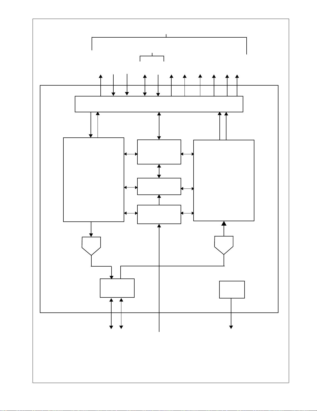
MII/RMII
DP83848K
SERIAL
MANAGEMENT
TX_CLK
TXD[3:0]
TX_EN
TX_DATA TX_CLK
MDIO
MDC
COL
MII/RMII INTERFACE
CRS/CRS_DV
RX_ER
RX_CLK
RX_DV
MII
10BASE-T & 10BASE-T &
Transmit
Block
Registers
Auto-Negotiation
State Machine
Receive
Block
RXD[3:0]
RX_CLK
RX_DATA
Clock
Generation
DAC
Auto-MDIX
ADC
LED
Driver
TD±
Figure 1. DP83848K Functional Block Diagram
LEDS
RD±
REFERENCE CLOCK
www.national.com 2

Table of Contents
1.0 Pin Descriptions . . . . . . . . . . . . . . . . . . . . . . . . . . . . . . . . . . . . . . . . . . . . . . . . . 9
1.1 Serial Management Interface . . . . . . . . . . . . . . . . . . . . . . . . . . . . . . . . . . . . . . . . . . . . . . .9
1.2 MAC Data Interface . . . . . . . . . . . . . . . . . . . . . . . . . . . . . . . . . . . . . . . . . . . . . . . . . . . . . .9
1.3 Clock Interface . . . . . . . . . . . . . . . . . . . . . . . . . . . . . . . . . . . . . . . . . . . . . . . . . . . . . . . . .10
1.4 LED Interface . . . . . . . . . . . . . . . . . . . . . . . . . . . . . . . . . . . . . . . . . . . . . . . . . . . . . . . . . .11
1.5 Reset . . . . . . . . . . . . . . . . . . . . . . . . . . . . . . . . . . . . . . . . . . . . . . . . . . . . . . . . . . . . . . . .11
1.6 Strap Options . . . . . . . . . . . . . . . . . . . . . . . . . . . . . . . . . . . . . . . . . . . . . . . . . . . . . . . . . .11
1.7 10 Mb/s and 100 Mb/s PMD Interface . . . . . . . . . . . . . . . . . . . . . . . . . . . . . . . . . . . . . . .13
1.8 Special Connections . . . . . . . . . . . . . . . . . . . . . . . . . . . . . . . . . . . . . . . . . . . . . . . . . . . . .13
1.9 Power Supply Pins . . . . . . . . . . . . . . . . . . . . . . . . . . . . . . . . . . . . . . . . . . . . . . . . . . . . . .13
1.10 Package Pin Assignments . . . . . . . . . . . . . . . . . . . . . . . . . . . . . . . . . . . . . . . . . . . . . . .14
2.0 Configuration . . . . . . . . . . . . . . . . . . . . . . . . . . . . . . . . . . . . . . . . . . . . . . . . . . 15
2.1 Auto-Negotiation . . . . . . . . . . . . . . . . . . . . . . . . . . . . . . . . . . . . . . . . . . . . . . . . . . . . . . . .15
2.1.1 Auto-Negotiation Pin Control . . . . . . . . . . . . . . . . . . . . . . . . . . . . . . . . . . . . . . . . . . . . . . . . . 15
2.1.2 Auto-Negotiation Register Control . . . . . . . . . . . . . . . . . . . . . . . . . . . . . . . . . . . . . . . . . . . . . 15
2.1.3 Auto-Negotiation Parallel Detection . . . . . . . . . . . . . . . . . . . . . . . . . . . . . . . . . . . . . . . . . . . . 16
2.1.4 Auto-Negotiation Restart . . . . . . . . . . . . . . . . . . . . . . . . . . . . . . . . . . . . . . . . . . . . . . . . . . . . 16
2.1.5 Auto-Negotiation Complete Time . . . . . . . . . . . . . . . . . . . . . . . . . . . . . . . . . . . . . . . . . . . . . . 16
2.2 Auto-MDIX . . . . . . . . . . . . . . . . . . . . . . . . . . . . . . . . . . . . . . . . . . . . . . . . . . . . . . . . . . . .16
2.3 PHY Address . . . . . . . . . . . . . . . . . . . . . . . . . . . . . . . . . . . . . . . . . . . . . . . . . . . . . . . . . .17
2.3.1 MII Isolate Mode . . . . . . . . . . . . . . . . . . . . . . . . . . . . . . . . . . . . . . . . . . . . . . . . . . . . . . . . . . 17
2.4 LED Interface . . . . . . . . . . . . . . . . . . . . . . . . . . . . . . . . . . . . . . . . . . . . . . . . . . . . . . . . . .18
2.4.1 LED . . . . . . . . . . . . . . . . . . . . . . . . . . . . . . . . . . . . . . . . . . . . . . . . . . . . . . . . . . . . . . . . . . . . 18
2.4.2 LED Direct Control . . . . . . . . . . . . . . . . . . . . . . . . . . . . . . . . . . . . . . . . . . . . . . . . . . . . . . . . . 18
2.5 Half Duplex vs. Full Duplex . . . . . . . . . . . . . . . . . . . . . . . . . . . . . . . . . . . . . . . . . . . . . . .19
2.6 Internal Loopback . . . . . . . . . . . . . . . . . . . . . . . . . . . . . . . . . . . . . . . . . . . . . . . . . . . . . . .19
2.7 BIST . . . . . . . . . . . . . . . . . . . . . . . . . . . . . . . . . . . . . . . . . . . . . . . . . . . . . . . . . . . . . . . . .19
3.0 Functional Description. . . . . . . . . . . . . . . . . . . . . . . . . . . . . . . . . . . . . . . . . . . 20
3.1 MII Interface . . . . . . . . . . . . . . . . . . . . . . . . . . . . . . . . . . . . . . . . . . . . . . . . . . . . . . . . . . .20
3.1.1 Nibble-wide MII Data Interface . . . . . . . . . . . . . . . . . . . . . . . . . . . . . . . . . . . . . . . . . . . . . . . . 20
3.1.2 Collision Detect . . . . . . . . . . . . . . . . . . . . . . . . . . . . . . . . . . . . . . . . . . . . . . . . . . . . . . . . . . . 20
3.1.3 Carrier Sense . . . . . . . . . . . . . . . . . . . . . . . . . . . . . . . . . . . . . . . . . . . . . . . . . . . . . . . . . . . . . 20
3.2 Reduced MII Interface . . . . . . . . . . . . . . . . . . . . . . . . . . . . . . . . . . . . . . . . . . . . . . . . . . .20
3.3 802.3u MII Serial Management Interface . . . . . . . . . . . . . . . . . . . . . . . . . . . . . . . . . . . . .21
3.3.1 Serial Management Register Access . . . . . . . . . . . . . . . . . . . . . . . . . . . . . . . . . . . . . . . . . . . 21
3.3.2 Serial Management Access Protocol . . . . . . . . . . . . . . . . . . . . . . . . . . . . . . . . . . . . . . . . . . . 21
3.3.3 Serial Management Preamble Suppression . . . . . . . . . . . . . . . . . . . . . . . . . . . . . . . . . . . . . 22
4.0 Architecture. . . . . . . . . . . . . . . . . . . . . . . . . . . . . . . . . . . . . . . . . . . . . . . . . . . . 23
4.1 100BASE-TX TRANSMITTER . . . . . . . . . . . . . . . . . . . . . . . . . . . . . . . . . . . . . . . . . . . . .23
4.1.1 Code-group Encoding and Injection . . . . . . . . . . . . . . . . . . . . . . . . . . . . . . . . . . . . . . . . . . . . 25
4.1.2 Scrambler . . . . . . . . . . . . . . . . . . . . . . . . . . . . . . . . . . . . . . . . . . . . . . . . . . . . . . . . . . . . . . . . 25
4.1.3 NRZ to NRZI Encoder . . . . . . . . . . . . . . . . . . . . . . . . . . . . . . . . . . . . . . . . . . . . . . . . . . . . . . 25
4.1.4 Binary to MLT-3 Convertor . . . . . . . . . . . . . . . . . . . . . . . . . . . . . . . . . . . . . . . . . . . . . . . . . . . 25
4.2 100BASE-TX RECEIVER . . . . . . . . . . . . . . . . . . . . . . . . . . . . . . . . . . . . . . . . . . . . . . . . .25
4.2.1 Analog Front End . . . . . . . . . . . . . . . . . . . . . . . . . . . . . . . . . . . . . . . . . . . . . . . . . . . . . . . . . . 25
4.2.2 Digital Signal Processor . . . . . . . . . . . . . . . . . . . . . . . . . . . . . . . . . . . . . . . . . . . . . . . . . . . . . 25
4.2.2.1 Digital Adaptive Equalization and Gain Control . . . . . . . . . . . . . . . . . . . . . . . . . . . . . . 27
4.2.2.2 Base Line Wander Compensation . . . . . . . . . . . . . . . . . . . . . . . . . . . . . . . . . . . . . . . . 28
4.2.3 Signal Detect . . . . . . . . . . . . . . . . . . . . . . . . . . . . . . . . . . . . . . . . . . . . . . . . . . . . . . . . . . . . . 28
4.2.4 MLT-3 to NRZI Decoder . . . . . . . . . . . . . . . . . . . . . . . . . . . . . . . . . . . . . . . . . . . . . . . . . . . . . 28
4.2.5 NRZI to NRZ . . . . . . . . . . . . . . . . . . . . . . . . . . . . . . . . . . . . . . . . . . . . . . . . . . . . . . . . . . . . . 28
4.2.6 Serial to Parallel . . . . . . . . . . . . . . . . . . . . . . . . . . . . . . . . . . . . . . . . . . . . . . . . . . . . . . . . . . . 28
4.2.7 Descrambler . . . . . . . . . . . . . . . . . . . . . . . . . . . . . . . . . . . . . . . . . . . . . . . . . . . . . . . . . . . . . . 29
4.2.8 Code-group Alignment . . . . . . . . . . . . . . . . . . . . . . . . . . . . . . . . . . . . . . . . . . . . . . . . . . . . . . 29
4.2.9 4B/5B Decoder . . . . . . . . . . . . . . . . . . . . . . . . . . . . . . . . . . . . . . . . . . . . . . . . . . . . . . . . . . . . 29
DP83848K
3 www.national.com

4.2.10 100BASE-TX Link Integrity Monitor . . . . . . . . . . . . . . . . . . . . . . . . . . . . . . . . . . . . . . . . . . . 29
4.2.11 Bad SSD Detection . . . . . . . . . . . . . . . . . . . . . . . . . . . . . . . . . . . . . . . . . . . . . . . . . . . . . . . 29
4.3 10BASE-T TRANSCEIVER MODULE . . . . . . . . . . . . . . . . . . . . . . . . . . . . . . . . . . . . . . .29
4.3.1 Operational Modes . . . . . . . . . . . . . . . . . . . . . . . . . . . . . . . . . . . . . . . . . . . . . . . . . . . . . . . . . 29
DP83848K
4.3.2 Smart Squelch . . . . . . . . . . . . . . . . . . . . . . . . . . . . . . . . . . . . . . . . . . . . . . . . . . . . . . . . . . . . 30
4.3.3 Collision Detection and SQE . . . . . . . . . . . . . . . . . . . . . . . . . . . . . . . . . . . . . . . . . . . . . . . . . 30
4.3.4 Carrier Sense . . . . . . . . . . . . . . . . . . . . . . . . . . . . . . . . . . . . . . . . . . . . . . . . . . . . . . . . . . . . . 30
4.3.5 Normal Link Pulse Detection/Generation . . . . . . . . . . . . . . . . . . . . . . . . . . . . . . . . . . . . . . . . 30
4.3.6 Jabber Function . . . . . . . . . . . . . . . . . . . . . . . . . . . . . . . . . . . . . . . . . . . . . . . . . . . . . . . . . . . 31
4.3.7 Automatic Link Polarity Detection and Correction . . . . . . . . . . . . . . . . . . . . . . . . . . . . . . . . . 31
4.3.8 Transmit and Receive Filtering . . . . . . . . . . . . . . . . . . . . . . . . . . . . . . . . . . . . . . . . . . . . . . . 31
4.3.9 Transmitter . . . . . . . . . . . . . . . . . . . . . . . . . . . . . . . . . . . . . . . . . . . . . . . . . . . . . . . . . . . . . . . 31
4.3.10 Receiver . . . . . . . . . . . . . . . . . . . . . . . . . . . . . . . . . . . . . . . . . . . . . . . . . . . . . . . . . . . . . . . . 31
5.0 Design Guidelines. . . . . . . . . . . . . . . . . . . . . . . . . . . . . . . . . . . . . . . . . . . . . . . 32
5.1 TPI Network Circuit . . . . . . . . . . . . . . . . . . . . . . . . . . . . . . . . . . . . . . . . . . . . . . . . . . . . . .32
5.2 ESD Protection . . . . . . . . . . . . . . . . . . . . . . . . . . . . . . . . . . . . . . . . . . . . . . . . . . . . . . . . .33
5.3 Clock In (X1) ReCommendations . . . . . . . . . . . . . . . . . . . . . . . . . . . . . . . . . . . . . . . . . . .33
5.4 Power Feedback Circuit . . . . . . . . . . . . . . . . . . . . . . . . . . . . . . . . . . . . . . . . . . . . . . . . . .35
5.5 Power Down . . . . . . . . . . . . . . . . . . . . . . . . . . . . . . . . . . . . . . . . . . . . . . . . . . . . . . . . . . .35
5.6 Energy Detect Mode . . . . . . . . . . . . . . . . . . . . . . . . . . . . . . . . . . . . . . . . . . . . . . . . . . . . .35
6.0 Reset Operation . . . . . . . . . . . . . . . . . . . . . . . . . . . . . . . . . . . . . . . . . . . . . . . . 35
6.1 Hardware Reset . . . . . . . . . . . . . . . . . . . . . . . . . . . . . . . . . . . . . . . . . . . . . . . . . . . . . . . .35
6.2 Software Reset . . . . . . . . . . . . . . . . . . . . . . . . . . . . . . . . . . . . . . . . . . . . . . . . . . . . . . . . .35
7.0 Register Block . . . . . . . . . . . . . . . . . . . . . . . . . . . . . . . . . . . . . . . . . . . . . . . . . 36
7.1 Register Definition . . . . . . . . . . . . . . . . . . . . . . . . . . . . . . . . . . . . . . . . . . . . . . . . . . . . . .39
7.1.1 Basic Mode Control Register (BMCR) . . . . . . . . . . . . . . . . . . . . . . . . . . . . . . . . . . . . . . . . . . 40
7.1.2 Basic Mode Status Register (BMSR) . . . . . . . . . . . . . . . . . . . . . . . . . . . . . . . . . . . . . . . . . . . 42
7.1.3 PHY Identifier Register #1 (PHYIDR1) . . . . . . . . . . . . . . . . . . . . . . . . . . . . . . . . . . . . . . . . . . 43
7.1.4 PHY Identifier Register #2 (PHYIDR2) . . . . . . . . . . . . . . . . . . . . . . . . . . . . . . . . . . . . . . . . . . 43
7.1.5 Auto-Negotiation Advertisement Register (ANAR) . . . . . . . . . . . . . . . . . . . . . . . . . . . . . . . . . 43
7.1.6 Auto-Negotiation Link Partner Ability Register (ANLPAR) (BASE Page) . . . . . . . . . . . . . . . . 45
7.1.7 Auto-Negotiation Link Partner Ability Register (ANLPAR) (Next Page) . . . . . . . . . . . . . . . . . 46
7.1.8 Auto-Negotiate Expansion Register (ANER) . . . . . . . . . . . . . . . . . . . . . . . . . . . . . . . . . . . . . 46
7.1.9 Auto-Negotiation Next Page Transmit Register (ANNPTR) . . . . . . . . . . . . . . . . . . . . . . . . . . 47
7.2 Extended Registers . . . . . . . . . . . . . . . . . . . . . . . . . . . . . . . . . . . . . . . . . . . . . . . . . . . . .48
7.2.1 PHY Status Register (PHYSTS) . . . . . . . . . . . . . . . . . . . . . . . . . . . . . . . . . . . . . . . . . . . . . . 48
7.2.2 False Carrier Sense Counter Register (FCSCR) . . . . . . . . . . . . . . . . . . . . . . . . . . . . . . . . . . 50
7.2.3 Receiver Error Counter Register (RECR) . . . . . . . . . . . . . . . . . . . . . . . . . . . . . . . . . . . . . . . 50
7.2.4 100 Mb/s PCS Configuration and Status Register (PCSR) . . . . . . . . . . . . . . . . . . . . . . . . . . 51
7.2.5 RMII and Bypass Register (RBR) . . . . . . . . . . . . . . . . . . . . . . . . . . . . . . . . . . . . . . . . . . . . . 52
7.2.6 LED Direct Control Register (LEDCR) . . . . . . . . . . . . . . . . . . . . . . . . . . . . . . . . . . . . . . . . . . 53
7.2.7 PHY Control Register (PHYCR) . . . . . . . . . . . . . . . . . . . . . . . . . . . . . . . . . . . . . . . . . . . . . . . 54
7.2.8 10Base-T Status/Control Register (10BTSCR) . . . . . . . . . . . . . . . . . . . . . . . . . . . . . . . . . . . 56
7.2.9 CD Test and BIST Extensions Register (CDCTRL1) . . . . . . . . . . . . . . . . . . . . . . . . . . . . . . . 57
7.2.10 Energy Detect Control (EDCR) . . . . . . . . . . . . . . . . . . . . . . . . . . . . . . . . . . . . . . . . . . . . . . 58
8.0 Electrical Specifications. . . . . . . . . . . . . . . . . . . . . . . . . . . . . . . . . . . . . . . . . . 59
8.1 DC Specs . . . . . . . . . . . . . . . . . . . . . . . . . . . . . . . . . . . . . . . . . . . . . . . . . . . . . . . . . . . . .59
8.2 AC Specs . . . . . . . . . . . . . . . . . . . . . . . . . . . . . . . . . . . . . . . . . . . . . . . . . . . . . . . . . . . . .61
8.2.1 Power Up Timing . . . . . . . . . . . . . . . . . . . . . . . . . . . . . . . . . . . . . . . . . . . . . . . . . . . . . . . . . . 61
8.2.2 Reset Timing . . . . . . . . . . . . . . . . . . . . . . . . . . . . . . . . . . . . . . . . . . . . . . . . . . . . . . . . . . . . . 62
8.2.3 MII Serial Management Timing . . . . . . . . . . . . . . . . . . . . . . . . . . . . . . . . . . . . . . . . . . . . . . . 63
8.2.4 100 Mb/s MII Transmit Timing . . . . . . . . . . . . . . . . . . . . . . . . . . . . . . . . . . . . . . . . . . . . . . . . 63
8.2.5 100 Mb/s MII Receive Timing . . . . . . . . . . . . . . . . . . . . . . . . . . . . . . . . . . . . . . . . . . . . . . . . 64
8.2.6 100BASE-TX Transmit Packet Latency Timing . . . . . . . . . . . . . . . . . . . . . . . . . . . . . . . . . . 64
8.2.7 100BASE-TX Transmit Packet Deassertion Timing . . . . . . . . . . . . . . . . . . . . . . . . . . . . . . . . 65
8.2.8 100BASE-TX Transmit Timing (tR/F & Jitter) . . . . . . . . . . . . . . . . . . . . . . . . . . . . . . . . . . . . . 66
8.2.9 100BASE-TX Receive Packet Latency Timing . . . . . . . . . . . . . . . . . . . . . . . . . . . . . . . . . . . 67
8.2.10 100BASE-TX Receive Packet Deassertion Timing . . . . . . . . . . . . . . . . . . . . . . . . . . . . . . . 67
8.2.11 10 Mb/s MII Transmit Timing . . . . . . . . . . . . . . . . . . . . . . . . . . . . . . . . . . . . . . . . . . . . . . . 68
8.2.12 10 Mb/s MII Receive Timing . . . . . . . . . . . . . . . . . . . . . . . . . . . . . . . . . . . . . . . . . . . . . . . . 68
www.national.com 4

8.2.13 10BASE-T Transmit Timing (Start of Packet) . . . . . . . . . . . . . . . . . . . . . . . . . . . . . . . . . . . 69
8.2.14 10BASE-T Transmit Timing (End of Packet) . . . . . . . . . . . . . . . . . . . . . . . . . . . . . . . . . . . . 69
8.2.15 10BASE-T Receive Timing (Start of Packet) . . . . . . . . . . . . . . . . . . . . . . . . . . . . . . . . . . . . 70
8.2.16 10BASE-T Receive Timing (End of Packet) . . . . . . . . . . . . . . . . . . . . . . . . . . . . . . . . . . . . . 70
8.2.17 10 Mb/s Heartbeat Timing . . . . . . . . . . . . . . . . . . . . . . . . . . . . . . . . . . . . . . . . . . . . . . . . . . 71
8.2.18 10 Mb/s Jabber Timing . . . . . . . . . . . . . . . . . . . . . . . . . . . . . . . . . . . . . . . . . . . . . . . . . . . . 71
8.2.19 10BASE-T Normal Link Pulse Timing . . . . . . . . . . . . . . . . . . . . . . . . . . . . . . . . . . . . . . . . . 72
8.2.20 Auto-Negotiation Fast Link Pulse (FLP) Timing . . . . . . . . . . . . . . . . . . . . . . . . . . . . . . . . . . 72
8.2.21 100BASE-TX Signal Detect Timing . . . . . . . . . . . . . . . . . . . . . . . . . . . . . . . . . . . . . . . . . . 73
8.2.22 100 Mb/s Internal Loopback Timing . . . . . . . . . . . . . . . . . . . . . . . . . . . . . . . . . . . . . . . . . . 73
8.2.23 10 Mb/s Internal Loopback Timing . . . . . . . . . . . . . . . . . . . . . . . . . . . . . . . . . . . . . . . . . . . 74
8.2.24 RMII Transmit Timing . . . . . . . . . . . . . . . . . . . . . . . . . . . . . . . . . . . . . . . . . . . . . . . . . . . . . 75
8.2.25 RMII Receive Timing . . . . . . . . . . . . . . . . . . . . . . . . . . . . . . . . . . . . . . . . . . . . . . . . . . . . . . 76
8.2.26 Isolation Timing . . . . . . . . . . . . . . . . . . . . . . . . . . . . . . . . . . . . . . . . . . . . . . . . . . . . . . . . . . 77
8.2.27 100 Mb/s X1 to TX_CLK Timing . . . . . . . . . . . . . . . . . . . . . . . . . . . . . . . . . . . . . . . . . . . . . 77
DP83848K
5 www.national.com

List of Figures
Figure 1. DP83848K Functional Block Diagram . . . . . . . . . . . . . . . . . . . . . . . . . . . . . . . . . . . . . . . . . . 2
DP83848K
Figure 2. PHYAD Strapping Example . . . . . . . . . . . . . . . . . . . . . . . . . . . . . . . . . . . . . . . . . . . . . . . . . 17
Figure 3. AN Strapping and LED Loading Example . . . . . . . . . . . . . . . . . . . . . . . . . . . . . . . . . . . . . . . 18
Figure 4. Typical MDC/MDIO Read Operation . . . . . . . . . . . . . . . . . . . . . . . . . . . . . . . . . . . . . . . . . . 22
Figure 5. Typical MDC/MDIO Write Operation . . . . . . . . . . . . . . . . . . . . . . . . . . . . . . . . . . . . . . . . . . . 22
Figure 6. 100BASE-TX Transmit Block Diagram . . . . . . . . . . . . . . . . . . . . . . . . . . . . . . . . . . . . . . . . . 23
Figure 7. 100BASE-TX Receive Block Diagram . . . . . . . . . . . . . . . . . . . . . . . . . . . . . . . . . . . . . . . . . 26
Figure 8. EIA/TIA Attenuation vs. Frequency for 0, 50, 100, 130 & 150 meters of CAT 5 cable . . . . . 27
Figure 9. 100BASE-TX BLW Event . . . . . . . . . . . . . . . . . . . . . . . . . . . . . . . . . . . . . . . . . . . . . . . . . . . 28
Figure 10. 10BASE-T Twisted Pair Smart Squelch Operation . . . . . . . . . . . . . . . . . . . . . . . . . . . . . . . 30
Figure 11. 10/100 Mb/s Twisted Pair Interface . . . . . . . . . . . . . . . . . . . . . . . . . . . . . . . . . . . . . . . . . . 32
Figure 12. Crystal Oscillator Circuit . . . . . . . . . . . . . . . . . . . . . . . . . . . . . . . . . . . . . . . . . . . . . . . . . . . 33
Figure 13. Power Feedback Connection . . . . . . . . . . . . . . . . . . . . . . . . . . . . . . . . . . . . . . . . . . . . . . . 35
www.national.com 6

List of Tables
Table 1. Auto-Negotiation Modes in DP83848K . . . . . . . . . . . . . . . . . . . . . . . . . . . . . . . . . . . . . . . . . . 15
Table 2. PHY Address Mapping . . . . . . . . . . . . . . . . . . . . . . . . . . . . . . . . . . . . . . . . . . . . . . . . . . . . . . 17
Table 3. LED Mode Select for DP83848K . . . . . . . . . . . . . . . . . . . . . . . . . . . . . . . . . . . . . . . . . . . . . . 18
Table 4. Supported packet sizes at +/-50ppm +/-100ppm for each clock . . . . . . . . . . . . . . . . . . . . . . 21
Table 5. Typical MDIO Frame Format . . . . . . . . . . . . . . . . . . . . . . . . . . . . . . . . . . . . . . . . . . . . . . . . . 21
Table 6. 4B5B Code-Group Encoding/Decoding . . . . . . . . . . . . . . . . . . . . . . . . . . . . . . . . . . . . . . . . . 24
Table 7. 25 MHz Oscillator Specification . . . . . . . . . . . . . . . . . . . . . . . . . . . . . . . . . . . . . . . . . . . . . . . 33
Table 8. 50 MHz Oscillator Specification . . . . . . . . . . . . . . . . . . . . . . . . . . . . . . . . . . . . . . . . . . . . . . . 34
Table 9. 25 MHz Crystal Specification . . . . . . . . . . . . . . . . . . . . . . . . . . . . . . . . . . . . . . . . . . . . . . . . . 34
Table 10. Register Map . . . . . . . . . . . . . . . . . . . . . . . . . . . . . . . . . . . . . . . . . . . . . . . . . . . . . . . . . . . . 36
Table 11. Register Table . . . . . . . . . . . . . . . . . . . . . . . . . . . . . . . . . . . . . . . . . . . . . . . . . . . . . . . . . . . 37
Table 12. Basic Mode Control Register (BMCR), address 0x00 . . . . . . . . . . . . . . . . . . . . . . . . . . . . . 40
Table 13. Basic Mode Status Register (BMSR), address 0x01 . . . . . . . . . . . . . . . . . . . . . . . . . . . . . . 42
Table 14. PHY Identifier Register #1 (PHYIDR1), address 0x02 . . . . . . . . . . . . . . . . . . . . . . . . . . . . . 43
Table 15. PHY Identifier Register #2 (PHYIDR2), address 0x03 . . . . . . . . . . . . . . . . . . . . . . . . . . . . . 43
Table 16. Negotiation Advertisement Register (ANAR), address 0x04 . . . . . . . . . . . . . . . . . . . . . . . . 43
Table 17. Auto-Negotiation Link Partner Ability Register (ANLPAR) (BASE Page), address 0x05 . . . 45
Table 18. Auto-Negotiation Link Partner Ability Register (ANLPAR) (Next Page), address 0x05 . . . . 46
Table 19. Auto-Negotiate Expansion Register (ANER), address 0x06 . . . . . . . . . . . . . . . . . . . . . . . . 46
Table 20. Auto-Negotiation Next Page Transmit Register (ANNPTR), address 0x07 . . . . . . . . . . . . . 47
Table 21. PHY Status Register (PHYSTS), address 0x10 . . . . . . . . . . . . . . . . . . . . . . . . . . . . . . . . . . 48
Table 22. False Carrier Sense Counter Register (FCSCR), address 0x14 . . . . . . . . . . . . . . . . . . . . . 50
Table 23. Receiver Error Counter Register (RECR), address 0x15 . . . . . . . . . . . . . . . . . . . . . . . . . . . 50
Table 24. 100 Mb/s PCS Configuration and Status Register (PCSR), address 0x16 . . . . . . . . . . . . . 51
Table 25. RMII and Bypass Register (RBR), addresses 0x17 . . . . . . . . . . . . . . . . . . . . . . . . . . . . . . . 52
Table 26. LED Direct Control Register (LEDCR), address 0x18 . . . . . . . . . . . . . . . . . . . . . . . . . . . . . 53
Table 27. PHY Control Register (PHYCR), address 0x19 . . . . . . . . . . . . . . . . . . . . . . . . . . . . . . . . . . 54
Table 28. 10Base-T Status/Control Register (10BTSCR), address 0x1A . . . . . . . . . . . . . . . . . . . . . . 56
Table 29. CD Test and BIST Extensions Register (CDCTRL1), address 0x1B . . . . . . . . . . . . . . . . . . 57
Table 30. Energy Detect Control (EDCR), address 0x1D . . . . . . . . . . . . . . . . . . . . . . . . . . . . . . . . . . 58
DP83848K
7 www.national.com

Pin Layout for DP83848K
DP83848K
RXD_2/PHYAD3
RXD_3/PHYAD4
RXD_0/PHYAD1
RXD_1/PHYAD2
RX_ER/MDIX_EN
COL/PHYAD0
CRS/CRS_DV/LED_CFG
RX_DV/MII_MODE
RX_CLK
31
32
33
PFBIN2
30
DGND
29
X1
28
X2
27
IOVDD33
26
MDC
25
MDIO
24
RESET_N
23
LED_LINK/AN0
19
PFBOUT
22
LED_SPEED/AN1
21
20
RBIAS
DAP
18
AVDD33
IOVDD33
TX_CLK
TX_EN
TXD_0
TXD_1
TXD_2
TXD_3
RESERVED
RESERVED
RESERVED
IOGND
34
35
36
37
38
39
40
1
2
3
4
5
6
7
8
9
10
11
RD -
DP83848K
15
14
13
12
TD +
TD -
AGND
RD +
16
PFBIN1
17
AGND
Note: Die Attached Pad (DAP) provides thermal dissipation, connection to GND plane recommended.
Top View
Order Number DP83848K
NS Package Number NSQAU040
www.national.com 8

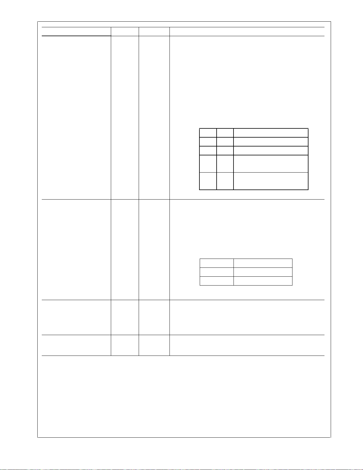
1.0 Pin Descriptions
The DP83848K pins are classified into the following interface categories (each interface is described in the sections
that follow):
— Serial Management Interface
— MAC Data Interface
— Clock Interface
— LED Interface
—Reset
— Strap Options
— 10/100 Mb/s PMD Interface
— Special Connect Pins
— Power and Ground pins
1.1 SERIAL MANAGEMENT INTERFACE
Signal Name Type Pin # Description
MDC I 25 MANAGEMENT DATA CLOCK: Synchronous clock to the MDIO
MDIO I/O 24 MANAGEMENT DATA I/O: Bi-directional management instruc-
Note: Strapping pin option. Please see Section 1.6 for strap
definitions.
All DP83848K signal pins are I/O cells regardless of the
particular use. The definitions below define the functionality
of the I/O cells for each pin.
Type: I Input
Type: O Output
Type: I/O Input/Output
Type: PD,PU Internal Pulldown/Pullup
Type: S Strapping Pin (All strap pins have weak in-
ternal pull-ups or pull-downs. If the default
strap value is needed to be changed then an
external 2.2 kΩ resistor should be used.
Please see Section 1.6 for details.)
management data input/output serial interface which may be
asynchronous to transmit and receive clocks. The maximum clock
rate is 25 MHz with no minimum clock rate.
tion/data signal that may be sourced by the station management
entity or the PHY. This pin requires a 1.5 kΩ pullup resistor.
DP83848K
1.2 MAC DATA INTERFACE
Signal Name Type Pin # Description
TX_CLK O 2 MII TRANSMIT CLOCK: 25 MHz Transmit clock output in 100
TX_EN I, PD 3 MII TRANSMIT ENABLE: Active high input indicates the pres-
TXD_0
TXD_1
TXD_2
TXD_3
RX_CLK O 31 MII RECEIVE CLOCK: Provides the 25 MHz recovered receive
RX_DV O, PD 32 MII RECEIVE DATA VALID: Asserted high to indicate that valid
I
I, PD
4
5
6
7
Mb/s mode or 2.5 MHz in 10 Mb/s mode derived from the 25 MHz
reference clock.
Unused in RMII mode. The device uses the X1 reference clock input as the 50 MHz reference for both transmit and receive.
ence of valid data inputs on TXD[3:0].
RMII TRANSMIT ENABLE: Active high input indicates the presence of valid data on TXD[1:0].
MII TRANSMIT DATA: Transmit data MII input pins, TXD[3:0],
that accept data synchronous to the TX_CLK (2.5 MHz in 10 Mb/s
mode or 25 MHz in 100 Mb/s mode).
RMII TRANSMIT DATA: Transmit data RMII input pins, TXD[1:0],
that accept data synchronous to the 50 MHz reference clock.
clocks for 100 Mb/s mode and 2.5 MHz for 10 Mb/s mode.
Unused in RMII mode. The device uses the X1 reference clock input as the 50 MHz reference for both transmit and receive.
data is present on the corresponding RXD[3:0].
RMII Synchronous Receive Data Valid: This signal provides the
RMII Receive Data Valid indication independent of Carrier Sense.
9 www.national.com

Signal Name Type Pin # Description
RX_ER S, O, PU 34 MII RECEIVE ERROR: Asserted high synchronously to RX_CLK
to indicate that an invalid symbol has been detected within a re-
DP83848K
RXD_0
RXD_1
RXD_2
RXD_3
CRS/CRS_DV S, O, PU 33 MII CARRIER SENSE: Asserted high to indicate the receive me-
COL S, O, PU 35 MII COLLISION DETECT: Asserted high to indicate detection of
S, O, PD 36
37
38
39
ceived packet in 100 Mb/s mode.
RMII RECEIVE ERROR: Assert high synchronously to X1 whenever it detects a media error and RX_DV is asserted in 100 Mb/s
mode.
This pin is not required to be used by a MAC, in either MII or RMII
mode, since the Phy is required to corrupt data on a receive error.
MII RECEIVE DATA: Nibble wide receive data signals driven synchronously to the RX_CLK, 25 MHz for 100 Mb/s mode, 2.5 MHz
for 10 Mb/s mode). RXD[3:0] signals contain valid data when
RX_DV is asserted.
RMII RECEIVE DATA: 2-bits receive data signals, RXD[1:0], driven synchronously to the X1 clock, 50 MHz.
dium is non-idle.
RMII CARRIER SENSE/RECEIVE DATA VALID: This signal
combines the RMII Carrier and Receive Data Valid indications.
For a detailed description of this signal, see the RMII Specification.
a collision condition (simultaneous transmit and receive activity)
in 10 Mb/s and 100 Mb/s Half Duplex Modes.
While in 10BASE-T Half Duplex mode with heartbeat enabled this
pin is also asserted for a duration of approximately 1µs at the end
of transmission to indicate heartbeat (SQE test).
In Full Duplex Mode, for 10 Mb/s or 100 Mb/s operation, this signal is always logic 0. There is no heartbeat function during 10
Mb/s full duplex operation.
RMII COLLISION DETECT: Per the RMII Specification, no COL
signal is required. The MAC will recover CRS from the CRS_DV
signal and use that along with its TX_EN signal to determine collision.
1.3 CLOCK INTERFACE
Signal Name Type Pin # Description
X1 I 28 CRYSTAL/OSCILLATOR INPUT: This pin is the primary clock
reference input for the DP83848K and must be connected to a 25
MHz 0.005% (+
either an external crystal resonator connected across pins X1 and
X2, or an external CMOS-level oscillator source connected to pin
X1 only.
RMII REFERENCE CLOCK: This pin is the primary clock reference input for the RMII mode and must be connected to a 50 MHz
0.005% (+50 ppm) CMOS-level oscillator source.
X2 O 27 CRYSTAL OUTPUT: This pin is the primary clock reference out-
put to connect to an external 25 MHz crystal resonator device.
This pin must be left unconnected if an external CMOS oscillator
clock source is used.
50 ppm) clock source. The DP83848K supports
www.national.com 10

1.4 LED INTERFACE
See Table 3 for LED Mode Selection.
Signal Name Type Pin # Description
LED_LINK S, O, PU 22 LINK LED: In Mode 1, this pin indicates the status of the LINK.
The LED will be ON when Link is good.
LINK/ACT LED: In Mode 2, this pin indicates transmit and receive
activity in addition to the status of the Link. The LED will be ON
when Link is good. It will blink when the transmitter or receiver is
active.
LED_SPEED S, O, PU 21 SPEED LED: This LED is ON when DP83848K is in 100Mb/s and
OFF when DP83848K is in 10Mb/s. Functionality of this LED is independent of the mode selected.
1.5 RESET
Signal Name Type Pin # Description
RESET_N I, PU 23 RESET: Active Low input that initializes or re-initializes the
DP83848K. Asserting this pin low for at least 1 µs will force a reset
process to occur. All internal registers will re-initialize to their default states as specified for each bit in the Register Block section.
All strap options are re-initialized as well.
DP83848K
1.6 STRAP OPTIONS
DP83848K uses many functional pins as strap options. The
values of these pins are sampled during reset and used to
strap the device into specific modes of operation. The strap
option pin assignments are defined below. The functional
pin name is indicated in parentheses.
Signal Name Type Pin # Description
PHYAD0 (COL)
PHYAD1 (RXD_0)
PHYAD2 (RXD_1)
PHYAD3 (RXD_2)
PHYAD4 (RXD_3)
S, O, PU
S, O, PD
35
36
37
38
39
PHY ADDRESS [4:0]: The DP83848K provides five PHY address
pins, the state of which are latched into the PHYCTRL register at
system Hardware-Reset.
The DP83848K supports PHY Address strapping values 0
(<00000>) through 31 (<11111>). A PHY Address of 0 puts the
part into the MII Isolate Mode. The MII isolate mode must be selected by strapping Phy Address 0; changing to Address 0 by register write will not put the Phy in the MII isolate mode. Please refer
to section 2.3 for additional information.
PHYAD0 pin has weak internal pull-up resistor.
PHYAD[4:1] pins have weak internal pull-down resistors.
A 2.2 kΩ resistor should be used for pull-down or pull-up to
change the default strap option. If the default option is
required, then there is no need for external pull-up or pull
down resistors. Since these pins may have alternate functions after reset is deasserted, they should not be connected directly to VCC or GND.
11 www.national.com
Signal Name Type Pin # Description
AN0 (LED_LINK)
AN1 (LED_SPEED)
DP83848K
S, O, PU
S, O, PU
22
21
These input pins control the advertised operating mode of the device according to the following table. The value on these pins are
set by connecting them to GND (0) or V
sistors. These pins should NEVER be connected directly to
GND or VCC.
The value set at this input is latched into the DP83848K at Hardware-Reset.
The float/pull-down status of these pins are latched into the Basic
Mode Control Register and the Auto_Negotiation Advertisement
Register during Hardware-Reset.
The default for DP83848K is 11 since these pins have an internal
pull-up.
AN1 AN0 Advertised Mode
0 0 10BASE-T, Half/Full-Duplex
0 1 100BASE-TX, Half/Full-Duplex
1 0 10BASE-T, Half-Duplex
100BASE-TX, Half-Duplex
1 1 10BASE-T, Half/Full-Duplex
100BASE-TX, Half/Full-Duplex
(1) through 2.2 kΩ re-
CC
MII_MODE (RX_DV) S, O, PD 32 MII MODE SELECT: This strapping option determines the oper-
LED_CFG (CRS/CRS_DV) S, O, PU 33 LED CONFIGURATION: This strapping option determines the
MDIX_EN (RX_ER) S, O, PU 34 MDIX ENABLE: Default is to enable MDIX. This strapping option
ating mode of the MAC Data Interface. Default operation (No pullup) will enable normal MII Mode of operation. Strapping
MII_MODE high will cause the device to be in RMII mode of operation. Since the pin includes an internal pull-down, the default value is 0.
The following table details the configuration:
MII_MODE MAC Interface Mode
0 MII Mode
1 RMII Mode
mode of operation of the LED pins. Default is Mode 1. Mode 1 and
Mode 2 can be controlled via the strap option. All modes are configurable via register access.
SeeTable 3 for LED Mode Selection.
disables Auto-MDIX. An external pull-down will disable AutoMDIX mode.
www.national.com 12

1.7 10 MB/S AND 100 MB/S PMD INTERFACE
Signal Name Type Pin # Description
TD-, TD+ I/O 14, 15 Differential common driver transmit output (PMD Output Pair).
RD-, RD+ I/O 11, 12 Differential receive input (PMD Input Pair). These differential in-
These differential outputs are automatically configured to either
10BASE-T or 100BASE-TX signaling.
In Auto-MDIX mode of operation, this pair can be used as the Receive Input pair.
These pins require 3.3V bias for operation.
puts are automatically configured to accept either 100BASE-TX
or 10BASE-T signaling.
In Auto-MDIX mode of operation, this pair can be used as the
Transmit Output pair.
These pins require 3.3V bias for operation.
1.8 SPECIAL CONNECTIONS
Signal Name Type Pin # Description
RBIAS I 20 Bias Resistor Connection. A 4.87 kΩ 1% resistor should be con-
PFBOUT O 19 Power Feedback Output. Parallel caps, 10µ F (Tantalum pre-
PFBIN1
PFBIN2
RESERVED I/O 8,9,10 RESERVED: These pins must be left unconnected.
I1630Power Feedback Input. These pins are fed with power from
nected from RBIAS to GND.
ferred) and 0.1µF, should be placed close to the PFBOUT. Con-
nect this pin to PFBIN1 (pin 16) and PFBIN2 (pin 30). See
Section 5.4 for proper placement pin.
PFBOUT pin. A small capacitor of 0.1µF should be connected
close to each pin.
Note: Do not supply power to these pins other than from
PFBOUT.
DP83848K
1.9 POWER SUPPLY PINS
Signal Name Pin # Description
IOVDD33 1, 26 I/O 3.3V Supply
IOGND 40 I/O Ground
DGND 29 Digital Ground
AVDD33 18 Analog 3.3V Supply
AGND 13, 17 Analog Ground
13 www.national.com

1.10 PACKAGE PIN ASSIGNMENTS
DP83848K
NSQAU040
Pin #
1IO_VDD
2TX_CLK
3TX_EN
4TXD_0
5TXD_1
6TXD_2
7TXD_3
8 RESERVED
9 RESERVED
10 RESERVED
11 RD-
12 RD+
13 AGND
14 TD -
15 TD +
16 PFBIN1
17 AGND
18 AVDD33
19 PFBOUT
20 RBIAS
21 LED_SPEED/AN1
22 LED_LINK/AN0
23 RESET_N
24 MDIO
25 MDC
26 IOVDD33
27 X2
28 X1
29 DGND
30 PFBIN2
31 RX_CLK
32 RX_DV/MII_MODE
33 CRS/CRS_DV/LED_CFG
34 RX_ER/MDIX_EN
35 COL/PHYAD0
36 RXD_0/PHYAD1
37 RXD_1/PHYAD2
38 RXD_2/PHYAD3
39 RXD_3/PHYAD4
40 IOGND
Pin Name
(DP83848K)
www.national.com 14

2.0 Configuration
This section includes information on the various configuration options available with the DP83848K. The configuration options described below include:
— Auto-Negotiation
— PHY Address and LED
— Half Duplex vs. Full Duplex
— Isolate mode
— Loopback mode
—BIST
2.1 AUTO-NEGOTIATION
The Auto-Negotiation function provides a mechanism for
exchanging configuration information between two ends of
a link segment and automatically selecting the highest performance mode of operation supported by both devices.
Fast Link Pulse (FLP) Bursts provide the signalling used to
communicate Auto-Negotiation abilities between two
devices at each end of a link segment. For further detail
regarding Auto-Negotiation, refer to Clause 28 of the IEEE
802.3u specification. The DP83848K supports four different Ethernet protocols (10 Mb/s Half Duplex, 10 Mb/s Full
Duplex, 100 Mb/s Half Duplex, and 100 Mb/s Full Duplex),
so the inclusion of Auto-Negotiation ensures that the highest performance protocol will be selected based on the
advertised ability of the Link Partner. In DP83848K, the
Auto-Negotiation function can be controlled either by internal register access or by the use of AN0 and AN1 pins.
2.1.1 Auto-Negotiation Pin Control
The state of AN0 and AN1 pins determine the specific
mode advertised by the device as given in Table 1.. The
state of AN0 and AN1 pins, upon power-up/reset, determines the state of bits [8:5] of the ANAR register.
The Auto-Negotiation function selected at power-up or
reset can be changed at any time by writing to the Basic
Mode Control Register (BMCR) at address 0x00h
Table 1. Auto-Negotiation Modes in DP83848K
AN1 AN0 Advertised Mode
0 0 10BASE-T, Half/Full-Duplex
0 1 100BASE-TX, Half/Full-Duplex
1 0 10BASE-T, Half-Duplex
100BASE-TX, Half-Duplex
1 1 10BASE-T, Half/Full-Duplex
100BASE-TX, Half/Full-Duplex
DP83848K
2.1.2 Auto-Negotiation Register Control
When Auto-Negotiation is enabled, the DP83848K transmits the abilities programmed into the Auto-Negotiation
Advertisement register (ANAR) at address 04h via FLP
Bursts. Any combination of 10 Mb/s, 100 Mb/s, HalfDuplex, and Full Duplex modes may be selected.
Auto-Negotiation Priority Resolution:
— (1) 100BASE-TX Full Duplex (Highest Priority)
— (2) 100BASE-TX Half Duplex
— (3) 10BASE-T Full Duplex
— (4) 10BASE-T Half Duplex (Lowest Priority)
The Basic Mode Control Register (BMCR) at address 00h
provides control for enabling, disabling, and restarting the
Auto-Negotiation process. When Auto-Negotiation is disabled, the Speed Selection bit in the BMCR controls
switching between 10 Mb/s or 100 Mb/s operation, and the
Duplex Mode bit controls switching between full duplex
operation and half duplex operation. The Speed Selection
and Duplex Mode bits have no effect on the mode of operation when the Auto-Negotiation Enable bit is set.
The Link Speed can be examined through the PHY Status
Register (PHYSTS) at address 10h after a Link is
achieved.
The Basic Mode Status Register (BMSR) indicates the set
of available abilities for technology types, Auto-Negotiation
ability, and Extended Register Capability. These bits are
permanently set to indicate the full functionality of the
DP83848K (only the 100BASE-T4 bit is not set since the
DP83848K does not support that function).
The BMSR also provides status on:
— Completion of Auto-Negotiation
— Occurrence of a remote fault as advertised by the Link
Partner
— Establishment of a valid link
— Support for Management Frame Preamble suppression
The Auto-Negotiation Advertisement Register (ANAR)
indicates the Auto-Negotiation abilities to be advertised by
the DP83848K. All available abilities are transmitted by
default, but any ability can be suppressed by writing to the
ANAR. Updating the ANAR to suppress an ability is one
way for a management agent to change (restrict) the technology that is used.
The Auto-Negotiation Link Partner Ability Register
(ANLPAR) at address 05h is used to receive the base link
code word as well as all next page code words during the
negotiation. Furthermore, the ANLPAR will be updated to
either 0081h or 0021h for parallel detection to either 100
Mb/s or 10 Mb/s respectively.
The Auto-Negotiation Expansion Register (ANER) indicates additional Auto-Negotiation status. The ANER provides status on:
— Occurrence of a Parallel Detect Fault
— Next Page function support by the Link Partner
— Next page support function by DP83848K
— Reception of the current page that is exchanged by Auto-
Negotiation
— Auto-Negotiation support by the Link Partner
15 www.national.com

2.1.3 Auto-Negotiation Parallel Detection
The DP83848K supports the Parallel Detection function
as defined in the IEEE 802.3u specification. Parallel
Detection requires both the 10 Mb/s and 100 Mb/s receiv-
DP83848K
ers to monitor the receive signal and report link status to
the Auto-Negotiation function. Auto-Negotiation uses this
information to configure the correct technology in the
event that the Link Partner does not support Auto-Negotiation but is transmitting link signals that the 100BASE-TX
or 10BASE-T PMAs recognize as valid link signals.
If the DP83848K completes Auto-Negotiation as a result
of Parallel Detection, bit 5 or bit 7 within the ANLPAR register will be set to reflect the mode of operation present in
the Link Partner. Note that bits 4:0 of the ANLPAR will also
be set to 00001 based on a successful parallel detection
to indicate a valid 802.3 selector field. Software may
determine that negotiation completed via Parallel Detection by reading a zero in the Link Partner Auto-Negotiation
Able bit once the Auto-Negotiation Complete bit is set. If
configured for parallel detect mode and any condition
other than a single good link occurs then the parallel
detect fault bit will be set.
2.1.4 Auto-Negotiation Restart
Once Auto-Negotiation has completed, it may be restarted
at any time by setting bit 9 (Restart Auto-Negotiation) of
the BMCR to one. If the mode configured by a successful
Auto-Negotiation loses a valid link, then the Auto-Negotiation process will resume and attempt to determine the
configuration for the link. This function ensures that a valid
configuration is maintained if the cable becomes disconnected.
A renegotiation request from any entity, such as a management agent, will cause the DP83848K to halt any
transmit data and link pulse activity until the
break_link_timer expires (~1500 ms). Consequently, the
Link Partner will go into link fail and normal Auto-Negotiation resumes. The DP83848K will resume Auto-Negotiation after the break_link_timer has expired by issuing FLP
(Fast Link Pulse) bursts.
2.1.5 Auto-Negotiation Complete Time
Parallel detection and Auto-Negotiation take approximately 2-3 seconds to complete. In addition, Auto-Negotiation with next page should take approximately 2-3
seconds to complete, depending on the number of next
pages sent.
Refer to Clause 28 of the IEEE 802.3u standard for a full
description of the individual timers related to Auto-Negotiation.
2.2 AUTO-MDIX
When enabled, this function utilizes Auto-Negotiation to
determine the proper configuration for transmission and
reception of data and subsequently selects the appropriate MDI pair for MDI/MDIX operation. The function uses a
random seed to control switching of the crossover circuitry. This implementation complies with the corresponding IEEE 802.3 Auto-Negotiation and Crossover
Specifications.
Auto-MDIX is enabled by default and can be configured
via strap or via PHYCR (0x19h) register, bits [15:14].
Neither Auto-Negotiation nor Auto-MDIX is required to be
enabled in forcing crossover of the MDI pairs. Forced
crossover can be achieved through the FORCE_MDIX bit,
bit 14 of PHYCR (0x19h) register.
Note: Auto-MDIX will not work in a forced mode of operation.
www.national.com 16
2.3 PHY ADDRESS
The 5 PHY address inputs pins are shared with the
RXD[3:0] pins and COL pin as shown below.
Table 2. PHY Address Mapping
Pin # PHYAD Function RXD Function
35 PHYAD0 COL
36 PHYAD1 RXD_0
37 PHYAD2 RXD_1
38 PHYAD3 RXD_2
39 PHYAD4 RXD_3
The DP83848K can be set to respond to any of 32 possible
PHY addresses via strap pins. The information is latched
into the PHYCR register (address 19h, bits [4:0]) at device
power-up and hardware reset. The PHY Address pins are
shared with the RXD and COL pins. Each DP83848K or
port sharing an MDIO bus in a system must have a unique
physical address.
The DP83848K supports PHY Address strapping values 0
(<0 0 0 0 0 >) throug h 3 1 ( <11111>). Strapping PHY Address
0 puts the part into Isolate Mode. It should also be noted
that selecting PHY Address 0 via an MDIO write to PHYCR
will not put the device in Isolate Mode. See Section 2.3.1
for more information.
For further detail relating to the latch-in timing requirements
of the PHY Address pins, as well as the other hardware
configuration pins, refer to the Reset summary in
Section 6.0.
DP83848K
Since the PHYAD[0] pin has weak internal pull-up resistor
and PHYAD[4:1] pins have weak internal pull-down resistors, the default setting for the PHY address is 00001
(01h).
Refer to Figure 2 for an example of a PHYAD connection to
external components. In this example, the PHYAD strapping results in address 00011 (03h).
2.3.1 MII Isolate Mode
The DP83848K can be put into MII Isolate mode by writing
to bit 10 of the BMCR register or by strapping in Physical
Address 0. It should be noted that selecting Physical
Address 0 via an MDIO write to PHYCR will not put the
device in the MII isolate mode.
When in the MII isolate mode, the DP83848K does not
respond to packet data present at TXD[3:0], TX_EN inputs
and presents a high impedance on the TX_CLK, RX_CLK,
RX_DV, RX_ER, RXD[3:0], COL, and CRS outputs. When
in Isolate mode, the DP83848K will continue to respond to
all management transactions.
While in Isolate mode, the PMD output pair will not transmit
packet data but will continue to source 100BASE-TX
scrambled idles or 10BASE-T normal link pulses.
The DP83848K can Auto-Negotiate or parallel detect to a
specific technology depending on the receive signal at the
PMD input pair. A valid link can be established for the
receiver even when the DP83848K is in Isolate mode.
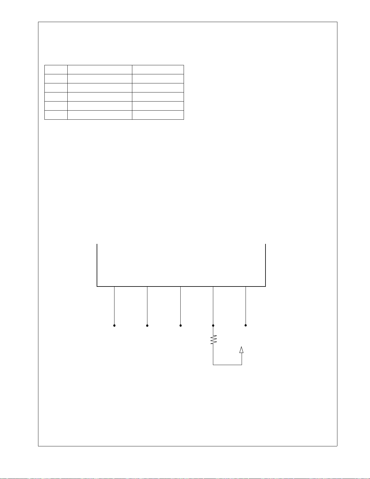
RXD_3
PHYAD4 = 0
RXD_2
PHYAD3 = 0
Figure 2. PHYAD Strapping Example
RXD_1
PHYAD2 = 0
RXD_0
PHYAD1 = 1
2.2kΩ
COL
PHYAD0 = 1
VCC
17 www.national.com

2.4 LED INTERFACE
The DP83848K supports configurable Light Emitting
Diode (LED) pins for configuring the link and speed. The
PHY Control Register (PHYCR) for the LED can also be
DP83848K
selected through address 19h, bit [5].
See Table 3. for LED Mode selection of DP83848K.
Table 3. LED Mode Select for DP83848K
LED_CFG
Mode
The LED_LINK pin in Mode 1 indicates the link status of
the port. In 100BASE-T mode, link is established as a
result of input receive amplitude compliant with the TPPMD specifications which will result in internal generation
of signal detect. A 10 Mb/s Link is established as a result
of the reception of at least seven consecutive normal Link
Pulses or the reception of a valid 10BASE-T packet. This
will cause the assertion of LED_LINK. LED_LINK will
deassert in accordance with the Link Loss Timer as specified in the IEEE 802.3 specification.
The LED_LINK pin in Mode 1 will be OFF when no LINK is
present.
The LED_LINK pin in Mode 2 will be ON to indicate Link is
good and BLINK to indicate activity is present on either
transmit or receive activity.
The LED_SPEED pin in DP83848K indicates 10 or 100
Mb/s data rate of the port. The standard CMOS driver
goes high when operating in 100Mb/s operation. The
functionality of this LED is independent of the mode
selected.
Since these LED pins are also used as strap options, the
polarity of the LED is dependent on whether the pin is
pulled up or down.
[0] (bit 5)
or (pin33)
1 1 ON for Good Link
2 0 ON for Good Link
LED_LINK LED_SPEED
OFF for No Link
BLINK for Activity
ON in 100Mb/s
OFF in 10Mb/s
ON in 100Mb/s
OFF in 10Mb/s
.
LED_SPEED
AN1 = 1
VCC
275Ω
Figure 3. AN Strapping and LED Loading Example
2.4.2 LED Direct Control
The DP83848K provides another option to directly control
the LED outputs through the LED Direct Control Register
(LEDCR), address 18h. The register does not provide
read access to the LED.
LED_LINK
AN0 = 0
2.2kΩ
275Ω
2.4.1 LED
Since the Auto-Negotiation strap options share the LED
output pins, the external components required for strapping and LED usage must be considered in order to avoid
contention.
Specifically, when the LED output is used to drive the LED
directly, the active state of the output driver is dependent
on the logic level sampled by the AN input upon powerup/reset. For example, if the AN input is resistively pulled
low then the corresponding output will be configured as an
active high driver. Conversely, if the AN input is resistively
pulled high, then the corresponding output will be configured as an active low driver.
Refer to Figure 3 for an example of AN connection to external components. In this example, the AN strapping results in Auto-Negotiation with 10BASE-T Half-Duplex ,
100BASE-TX, Half-Duplex advertised.
The adaptive nature of the LED output helps to simplify
potential implementation issues of this dual purpose pin.
www.national.com 18

2.5 HALF DUPLEX VS. FULL DUPLEX
The DP83848K supports both half and full duplex operation
at both 10 Mb/s and 100 Mb/s speeds.
Half-duplex relies on the CSMA/CD protocol to handle collisions and network access. In Half-Duplex mode, CRS
responds to both transmit and receive activity in order to
maintain compliance with the IEEE 802.3 specification.
Since the DP83848K is designed to support simultaneous
transmit and receive activity, it is capable of supporting fullduplex switched applications with a throughput of up to 200
Mb/s per port when operating in 100BASE-TX mode.
Because the CSMA/CD protocol does not apply to fullduplex operation, the DP83848K disables its own internal
collision sensing and reporting functions and modifies the
behavior of Carrier Sense (CRS) such that it indicates only
receive activity. This allows a full-duplex capable MAC to
operate properly.
All modes of operation (100BASE-TX and 10BASE-T) can
run either half-duplex or full-duplex. Additionally, other than
CRS and Collision reporting, all remaining MII signaling
remains the same regardless of the selected duplex mode.
It is important to understand that while Auto-Negotiation
with the use of Fast Link Pulse code words can interpret
and configure to full-duplex operation, parallel detection
can not recognize the difference between full and halfduplex from a fixed 10 Mb/s or 100 Mb/s link partner over
twisted pair. As specified in the 802.3u specification, if a
far-end link partner is configured to a forced full duplex
100BASE-TX ability, the parallel detection state machine in
the partner would be unable to detect the full duplex capability of the far-end link partner. This link segment would
negotiate to a half duplex 100BASE-TX configuration
(same scenario for 10 Mb/s).
2.6 INTERNAL LOOPBACK
The DP83848K includes a Loopback Test mode for facilitating system diagnostics. The Loopback mode is selected
DP83848K
through bit 14 (Loopback) of the Basic Mode Control Register (BMCR). Writing 1 to this bit enables MII transmit data
to be routed to the MII receive outputs. Loopback status
may be checked in bit 3 of the PHY Status Register
(PHYSTS). While in Loopback mode the data will not be
transmitted onto the media. To ensure that the desired
operating mode is maintained, Auto-Negotiation should be
disabled before selecting the Loopback mode.
2.7 BIST
The DP83848K incorporates an internal Built-in Self Test
(BIST) circuit to accommodate in-circuit testing or diagnostics. The BIST circuit can be utilized to test the integrity of
the transmit and receive data paths. BIST testing can be
performed with the part in the internal loopback mode or
externally looped back using a loopback cable fixture.
The BIST is implemented with independent transmit and
receive paths, with the transmit block generating a continuous stream of a pseudo random sequence. The user can
select a 9 bit or 15 bit pseudo random sequence from the
PSR_15 bit in the PHY Control Register (PHYCR). The
received data is compared to the generated pseudo-random data by the BIST Linear Feedback Shift Register
(LFSR) to determine the BIST pass/fail status.
The pass/fail status of the BIST is stored in the BIST status
bit in the PHYCR register. The status bit defaults to 0 (BIST
fail) and will transition on a successful comparison. If an
error (mis-compare) occurs, the status bit is latched and is
cleared upon a subsequent write to the Start/Stop bit.
For transmit VOD testing, the Packet BIST Continuous
Mode can be used to allow continuous data transmission,
setting BIST_CONT_MODE, bit 5, of CDCTRL1 (0x1Bh).
The number of BIST errors can be monitored through the
BIST Error Count in the CDCTRL1 (0x1Bh), bits [15:8].
19 www.national.com

3.0 Functional Description
The DP83848K supports two modes of operation using
the MII interface pins. The options are defined in the following sections and include:
DP83848K
—MII Mode
— RMII Mode
The modes of operation can be selected by strap options
or register control. For RMII mode, it is required to use the
strap option, since it requires a 50 MHz clock instead of
the normal 25 MHz.
In the each of these modes, the IEEE 802.3 serial management interface is operational for device configuration
and status. The serial management interface of the MII
allows for the configuration and control of multiple PHY
devices, gathering of status, error information, and the
determination of the type and capabilities of the attached
PHY(s).
3.1 MII INTERFACE
The DP83848K incorporates the Media Independent Interface (MII) as specified in Clause 22 of the IEEE 802.3u
standard. This interface may be used to connect PHY
devices to a MAC in 10/100 Mb/s systems. This section
describes the nibble wide MII data interface.
The nibble wide MII data interface consists of a receive
bus and a transmit bus each with control signals to facilitate data transfer between the PHY and the upper layer
(MAC).
active simultaneously. Collisions are reported by the COL
signal on the MII.
If the DP83848K is transmitting in 10 Mb/s mode when a
collision is detected, the collision is not reported until
seven bits have been received while in the collision state.
This prevents a collision being reported incorrectly due to
noise on the network. The COL signal remains set for the
duration of the collision.
If a collision occurs during a receive operation, it is immediately reported by the COL signal.
When heartbeat is enabled (only applicable to 10 Mb/s
operation), approximately 1µs after the transmission of
each packet, a Signal Quality Error (SQE) signal of
approximately 10 bit times is generated (internally) to indicate successful transmission. SQE is reported as a pulse
on the COL signal of the MII.
3.1.3 Carrier Sense
Carrier Sense (CRS) is asserted due to receive activity,
once valid data is detected via the squelch function during
10 Mb/s operation. During 100 Mb/s operation CRS is
asserted when a valid link (SD) and two non-contiguous
zeros are detected on the line.
For 10 or 100 Mb/s Half Duplex operation, CRS is
asserted during either packet transmission or reception.
For 10 or 100 Mb/s Full Duplex operation, CRS is
asserted only due to receive activity.
CRS is deasserted following an end of packet.
3.1.1 Nibble-wide MII Data Interface
Clause 22 of the IEEE 802.3u specification defines the
Media Independent Interface. This interface includes a
dedicated receive bus and a dedicated transmit bus.
These two data buses, along with various control and status signals, allow for the simultaneous exchange of data
between the DP83848K and the upper layer agent (MAC).
The receive interface consists of a nibble wide data bus
RXD[3:0], a receive error signal RX_ER, a receive data
valid flag RX_DV, and a receive clock RX_CLK for synchronous transfer of the data. The receive clock operates
at either 2.5 MHz to support 10 Mb/s operation modes or
at 25 MHz to support 100 Mb/s operational modes.
The transmit interface consists of a nibble wide data bus
TXD[3:0], a transmit enable control signal TX_EN, and a
transmit clock TX_CLK which runs at either 2.5 MHz or 25
MHz.
Additionally, the MII includes the carrier sense signal
CRS, as well as a collision detect signal COL. The CRS
signal asserts to indicate the reception of data from the
network or as a function of transmit data in Half Duplex
mode. The COL signal asserts as an indication of a collision which can occur during half-duplex operation when
both a transmit and receive operation occur simultaneously.
3.1.2 Collision Detect
For Half Duplex, a 10BASE-T or 100BASE-TX collision is
detected when the receive and transmit channels are
3.2 Reduced MII Interface
The DP83848T incorporates the Reduced Media Independent Interface (RMII) as specified in the RMII specification
(rev1.2) from the RMII Consortium. This interface may be
used to connect PHY devices to a MAC in 10/100 Mb/s
systems using a reduced number of pins. In this mode,
data is transferred 2-bits at a time using the 50 MHz
RMII_REF clock for both transmit and receive. The following pins are used in RMII mode:
— TX_EN
— TXD[1:0]
— RX_ER (optional for Mac)
— CRS_DV
— RXD[1:0]
— X1 (RMII Reference clock is 50 MHz)
In addition, the RMII mode supplies an RX_DV signal
which allows for a simpler method of recovering receive
data without having to separate RX_DV from the CRS_DV
indication. This is especially useful for systems which do
not require CRS, such as systems that only support fullduplex operation. This signal is also useful for diagnostic
testing where it may be desirable to loop Receive RMII
data directly to the transmitter.
Since the reference clock operates at 10 times the data
rate for 10 Mb/s operation, transmit data is sampled every
10 clocks. Likewise, receive data will be generated every
10th clock so that an attached device can sample the data
every 10 clocks.
www.national.com 20

RMII mode requires a 50 MHz oscillator be connected to
the device X1 pin. A 50 MHz crystal is not supported.
To tolerate potential frequency differences between the 50
MHz reference clock and the recovered receive clock, the
receive RMII function includes a programmable elasticity
buffer. The elasticity buffer is programmable to minimize
propagation delay based on expected packet size and
clock accuracy. This allows for supporting a range of
packet sizes including jumbo frames.
Table 4. Supported packet sizes at +/-50ppm +/-100ppm for each clock
Start Threshold
RBR[1:0]
1 (4-bits) 2 bits 2400 bytes 1200 bytes
2 (8-bits) 6 bits 7200 bytes 3600 bytes
3 (12-bits) 10 bits 12000 bytes 6000 bytes
0 (16-bits) 14 bits 16800 bytes 8400 bytes
Latency Tolerance Recommended Packet Size
The elasticity buffer will force Frame Check Sequence
errors for packets which overrun or underrun the FIFO.
Underrun and Overrun conditions can be reported in the
RMII and Bypass Register (RBR). The following table indicates how to program the elasticity buffer fifo (in 4-bit increments) based on expected max packet size and clock
accuracy. It assumes both clocks (RMII Reference clock
and far-end Transmitter clock) have the same accuracy.
Recommended Packet Size
at +/- 50ppm
DP83848K
at +/- 100ppm
3.3 802.3U MII SERIAL MANAGEMENT INTERFACE
3.3.1 Serial Management Register Access
The serial management MII specification defines a set of
thirty-two 16-bit status and control registers that are accessible through the management interface pins MDC and
MDIO. The DP83848K implements all the required MII registers as well as several optional registers. These registers
are fully described in Section 7.0. A description of the serial
management access protocol follows.
3.3.2 Serial Management Access Protocol
The serial control interface consists of two pins, Management Data Clock (MDC) and Management Data Input/Output (MDIO). MDC has a maximum clock rate of 25 MHz
and no minimum rate. The MDIO line is bi-directional and
may be shared by up to 32 devices. The MDIO frame format is shown below in Table 5..
The MDIO pin requires a pull-up resistor (1.5 kΩ) which,
during IDLE and turnaround, will pull MDIO high. In order to
initialize the MDIO interface, the station management entity
sends a sequence of 32 contiguous logic ones on MDIO to
provide the DP83848K with a sequence that can be used
to establish synchronization. This preamble may be generated either by driving MDIO high for 32 consecutive MDC
clock cycles, or by simply allowing the MDIO pull-up resistor to pull the MDIO pin high during which time 32 MDC
clock cycles are provided. In addition, 32 MDC clock cycles
should be used to re-sync the device if an invalid start,
opcode, or turnaround bit is detected.
The DP83848K waits until it has received this preamble
sequence before responding to any other transaction.
Once the DP83848K serial management port has been initialized no further preamble sequencing is required until
after a power-on/reset, invalid Start, invalid Opcode, or
invalid turnaround bit has occurred.
The Start code is indicated by a <01> pattern. This assures
the MDIO line transitions from the default idle line state.
Turnaround is defined as an idle bit time inserted between
the Register Address field and the Data field. To avoid contention during a read transaction, no device shall actively
drive the MDIO signal during the first bit of Turnaround.
The addressed DP83848K drives the MDIO with a zero for
the second bit of turnaround and follows this with the
required data. Figure 4 shows the timing relationship
between MDC and the MDIO as driven/received by the Station (STA) and the DP83848K (PHY) for a typical register
read access.
For write transactions, the station management entity
writes data to the addressed DP83848K thus eliminating
the requirement for MDIO Turnaround. The Turnaround
time is filled by the management entity by inserting <10>.
Figure 5 shows the timing relationship for a typical MII register write access.
Table 5. Typical MDIO Frame Format
MII Management
Serial Protocol
Read Operation <idle><01><10><AAAAA><RRRRR><Z0><xxxx xxxx xxxx xxxx><idle>
Write Operation <idle><01><01><AAAAA><RRRRR><10><xxxx xxxx xxxx xxxx><idle>
<idle><start><op code><device addr><reg addr><turnaround><data><idle>
21 www.national.com
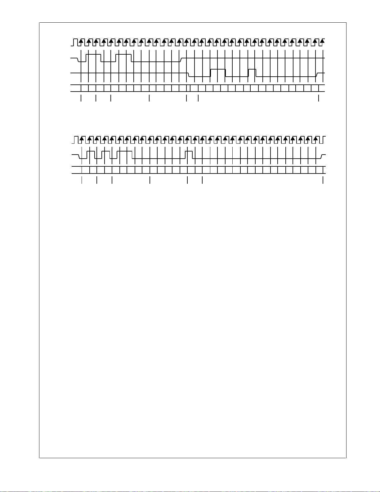
MDC
DP83848K
MDIO
MDIO
(STA)
(PHY)
Z
Z
00011 110000000
Idle Start
Opcode
(Read)
PHY Address
(PHYAD = 0Ch)
Register Address
(00h = BMCR)
Figure 4. Typical MDC/MDIO Read Operation
MDC
MDIO
(STA)
Z
00011110000000
Idle Start
Opcode
(Write)
PHY Address
(PHYAD = 0Ch)
Register Address
(00h = BMCR)
Figure 5. Typical MDC/MDIO Write Operation
3.3.3 Serial Management Preamble Suppression
The DP83848K supports a Preamble Suppression mode
as indicated by a one in bit 6 of the Basic Mode Status
Register (BMSR, address 01h.) If the station management
entity (i.e. MAC or other management controller) determines that all PHYs in the system support Preamble Suppression by returning a one in this bit, then the station
management entity need not generate preamble for each
management transaction.
The DP83848K requires a single initialization sequence of
32 bits of preamble following hardware/software reset.
This requirement is generally met by the mandatory pullup resistor on MDIO in conjunction with a continuous
MDC, or the management access made to determine
whether Preamble Suppression is supported.
While the DP83848K requires an initial preamble
sequence of 32 bits for management initialization, it does
not require a full 32-bit sequence between each subsequent transaction. A minimum of one idle bit between
management transactions is required as specified in the
IEEE 802.3u specification.
Z
Z
Z
0 0 011000100000000
TA
0 0 0 000 00000000
1000
TA
Register Data
Register Data
Z
Z
Idle
ZZ
Z
Idle
www.national.com 22
4.0 Architecture
This section describes the operations within each transceiver module, 100BASE-TX and 10BASE-T. Each operation consists of several functional blocks and described in
the following:
— 100BASE-TX Transmitter
— 100BASE-TX Receiver
— 10BASE-T Transceiver Module
4.1 100BASE-TX TRANSMITTER
The 100BASE-TX transmitter consists of several functional
blocks which convert synchronous 4-bit nibble data, as provided by the MII, to a scrambled MLT-3 125 Mb/s serial
data stream. Because the 100BASE-TX TP-PMD is integrated, the differential output pins, PMD Output Pair, can
be directly routed to the magnetics.
DP83848K
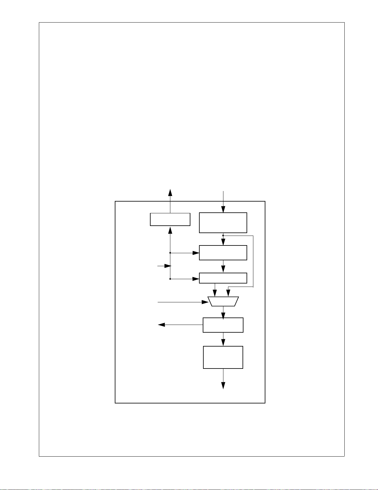
The block diagram in Figure 6. provides an overview of
each functional block within the 100BASE-TX transmit section.
The Transmitter section consists of the following functional
blocks:
— Code-group Encoder and Injection block
— Scrambler block (bypass option)
— NRZ to NRZI encoder block
— Binary to MLT-3 converter / Common Driver
The bypass option for the functional blocks within the
100BASE-TX transmitter provides flexibility for applications
where data conversion is not always required. The
DP83848K implements the 100BASE-TX transmit state
machine diagram as specified in the IEEE 802.3u Standard, Clause 24.
125MHZ CLOCK
BP_SCR
100BASE-TX
LOOPBACK
TX_CLK TXD[3:0] /
DIVIDE
BY 5
MLT[1:0]
TX_EN
4B5B CODE-GROUP
ENCODER &
INJECTOR
5B PARALLEL
TO SERIAL
SCRAMBLER
MUX
NRZ TO NRZI
ENCODER
BINARY
TO MLT-3 /
COMMON
DRIVER
PMD OUTPUT PAIR
Figure 6. 100BASE-TX Transmit Block Diagram
23 www.national.com

Table 6. 4B5B Code-Group Encoding/Decoding
DATA CODES
DP83848K
IDLE AND CONTROL CODES
INVALID CODES
Note: Control code-groups I, J, K, T and R in data fields will be mapped as invalid codes, together with RX_ER asserted.
0 11110 0000
1 01001 0001
2 10100 0010
3 10101 0011
4 01010 0100
5 01011 0101
6 01110 0110
7 01111 0111
8 10010 1000
9 10011 1001
A 10110 1010
B 10111 1011
C 11010 1100
D 11011 1101
E 11100 1110
F 11101 1111
H 00100 HALT code-group - Error code
I 11111 Inter-Packet IDLE - 0000 (
J 11000 First Start of Packet - 0101 (Note 1)
K 10001 Second Start of Packet - 0101 (Note 1)
T 01101 First End of Packet - 0000 (Note 1)
R 00111 Second End of Packet - 0000 (Note 1)
V 00000
V 00001
V 00010
V 00011
V 00101
V 00110
V 01000
V 01100
Note 1)
www.national.com 24

4.1.1 Code-group Encoding and Injection
The code-group encoder converts 4-bit (4B) nibble data
generated by the MAC into 5-bit (5B) code-groups for
transmission. This conversion is required to allow control
data to be combined with packet data code-groups. Refer
to Table 6. for 4B to 5B code-group mapping details.
The code-group encoder substitutes the first 8-bits of the
MAC preamble with a J/K code-group pair (11000 10001)
upon transmission. The code-group encoder continues to
replace subsequent 4B preamble and data nibbles with
corresponding 5B code-groups. At the end of the transmit
packet, upon the deassertion of Transmit Enable signal
from the MAC, the code-group encoder injects the T/R
code-group pair (01101 00111) indicating the end of the
frame.
After the T/R code-group pair, the code-group encoder
continuously injects IDLEs into the transmit data stream
until the next transmit packet is detected (reassertion of
Transmit Enable).
4.1.2 Scrambler
The scrambler is required to control the radiated emissions
at the media connector and on the twisted pair cable (for
100BASE-TX applications). By scrambling the data, the
total energy launched onto the cable is randomly distributed over a wide frequency range. Without the scrambler,
energy levels at the PMD and on the cable could peak
beyond FCC limitations at frequencies related to repeating
5B sequences (i.e., continuous transmission of IDLEs).
The scrambler is configured as a closed loop linear feedback shift register (LFSR) with an 11-bit polynomial. The
output of the closed loop LFSR is X-ORd with the serial
NRZ data from the code-group encoder. The result is a
scrambled data stream with sufficient randomization to
decrease radiated emissions at certain frequencies by as
much as 20 dB. The DP83848K uses the PHY_ID (pins
PHYAD [4:0]) to set a unique seed value.
DP83848K
transmit transformer primary winding, resulting in a MLT-3
signal.
The 100BASE-TX MLT-3 signal sourced by the PMD Output Pair common driver is slew rate controlled. This should
be considered when selecting AC coupling magnetics to
ensure TP-PMD Standard compliant transition times (3 ns
< Tr < 5 ns).
The 100BASE-TX transmit TP-PMD function within the
DP83848K is capable of sourcing only MLT-3 encoded
data. Binary output from the PMD Output Pair is not possible in 100 Mb/s mode.
4.2 100BASE-TX RECEIVER
The 100BASE-TX receiver consists of several functional
blocks which convert the scrambled MLT-3 125 Mb/s serial
data stream to synchronous 4-bit nibble data that is provided to the MII. Because the 100BASE-TX TP-PMD is
integrated, the differential input pins, RD±, can be directly
routed from the AC coupling magnetics.
See Figure 7 for a block diagram of the 100BASE-TX
receive function. This provides an overview of each functional block within the 100BASE-TX receive section.
The Receive section consists of the following functional
blocks:
— Analog Front End
— Digital Signal Processor
— Signal Detect
— MLT-3 to Binary Decoder
— NRZI to NRZ Decoder
— Serial to Parallel
— Descrambler
— Code Group Alignment
—4B/5B Decoder
— Link Integrity Monitor
— Bad SSD Detection
4.1.3 NRZ to NRZI Encoder
After the transmit data stream has been serialized and
scrambled, the data must be NRZI encoded in order to
comply with the TP-PMD standard for 100BASE-TX transmission over Category-5 Unshielded twisted pair cable.
4.1.4 Binary to MLT-3 Convertor
The Binary to MLT-3 conversion is accomplished by converting the serial binary data stream output from the NRZI
encoder into two binary data streams with alternately
phased logic one events. These two binary streams are
then fed to the twisted pair output driver which converts the
voltage to current and alternately drives either side of the
4.2.1 Analog Front End
In addition to the Digital Equalization and Gain Control, the
DP83848K includes Analog Equalization and Gain Control
in the Analog Front End. The Analog Equalization reduces
the amount of Digital Equalization required in the DSP.
4.2.2 Digital Signal Processor
The Digital Signal Processor includes Adaptive Equalization with Gain Control and Base Line Wander Compensation.
25 www.national.com

DP83848K
RX_DV/CRS
RX_CLK RXD[3:0] / RX_ER
4B/5B DECODER
SERIAL TO
PARALLEL
RX _DATA VAL ID
SSD DETECT
CODE GROUP
ALIGNMENT
DESCRAMBLER
NRZI TO NRZ
DECODER
MLT-3 TO BINARY
DECODER
DIGITAL
SIGNAL
PROCESSOR
ANALOG
FRONT
END
LINK
INTEGRITY
MONITOR
SIGNAL
DETECT
RD +/−
Figure 7. 100BASE-TX Receive Block Diagram
www.national.com 26

4.2.2.1 Digital Adaptive Equalization and Gain Control
When transmitting data at high speeds over copper twisted
pair cable, frequency dependent attenuation becomes a
concern. In high-speed twisted pair signalling, the frequency content of the transmitted signal can vary greatly
during normal operation based primarily on the randomness of the scrambled data stream. This variation in signal
attenuation caused by frequency variations must be compensated to ensure the integrity of the transmission.
In order to ensure quality transmission when employing
MLT-3 encoding, the compensation must be able to adapt
to various cable lengths and cable types depending on the
installed environment. The selection of long cable lengths
for a given implementation, requires significant compensation which will over-compensate for shorter, less attenuating lengths. Conversely, the selection of short or
intermediate cable lengths requiring less compensation will
cause serious under-compensation for longer length
cables. The compensation or equalization must be adap-
DP83848K
tive to ensure proper conditioning of the received signal
independent of the cable length.
The DP83848K utilizes an extremely robust equalization
scheme referred as ‘Digital Adaptive Equalization.’
The Digital Equalizer removes ISI (inter symbol interference) from the receive data stream by continuously adapting to provide a filter with the inverse frequency response
of the channel. Equalization is combined with an adaptive
gain control stage. This enables the receive 'eye pattern' to
be opened sufficiently to allow very reliable data recovery.
The curves given in Figure 8 illustrate attenuation at certain
frequencies for given cable lengths. This is derived from
the worst case frequency vs. attenuation figures as specified in the EIA/TIA Bulletin TSB-36. These curves indicate
the significant variations in signal attenuation that must be
compensated for by the receive adaptive equalization circuit.
Figure 8. EIA/TIA Attenuation vs. Frequency for 0, 50,
100, 130 & 150 meters of CAT 5 cable
27 www.national.com

4.2.2.2 Base Line Wander Compensation
DP83848K
Figure 9. 100BASE-TX BLW Event
The DP83848K is completely ANSI TP-PMD compliant
and includes Base Line Wander (BLW) compensation.
The BLW compensation block can successfully recover
the TP-PMD defined “killer” pattern.
BLW can generally be defined as the change in the average DC content, relatively short period over time, of an AC
coupled digital transmission over a given transmission
medium. (i.e., copper wire).
BLW results from the interaction between the low frequency components of a transmitted bit stream and the
frequency response of the AC coupling component(s)
within the transmission system. If the low frequency content of the digital bit stream goes below the low frequency
pole of the AC coupling transformers then the droop characteristics of the transformers will dominate resulting in
potentially serious BLW.
The digital oscilloscope plot provided in Figure 9 illustrates the severity of the BLW event that can theoretically
be generated during 100BASE-TX packet transmission.
This event consists of approximately 800 mV of DC offset
for a period of 120 µs. Left uncompensated, events such
as this can cause packet loss.
4.2.3 Signal Detect
The signal detect function of the DP83848K is incorporated to meet the specifications mandated by the ANSI
FDDI TP-PMD Standard as well as the IEEE 802.3
100BASE-TX Standard for both voltage thresholds and
timing parameters.
Note that the reception of normal 10BASE-T link pulses
and fast link pulses per IEEE 802.3u Auto-Negotiation by
the 100BASE-TX receiver do not cause the DP83848K to
assert signal detect.
4.2.4 MLT-3 to NRZI Decoder
The DP83848K decodes the MLT-3 information from the
Digital Adaptive Equalizer block to binary NRZI data.
4.2.5 NRZI to NRZ
In a typical application, the NRZI to NRZ decoder is
required in order to present NRZ formatted data to the
descrambler.
4.2.6 Serial to Parallel
The 100BASE-TX receiver includes a Serial to Parallel
converter which supplies 5-bit wide data symbols to the
PCS Rx state machine.
www.national.com 28

4.2.7 Descrambler
A serial descrambler is used to de-scramble the received
NRZ data. The descrambler has to generate an identical
data scrambling sequence (N) in order to recover the original unscrambled data (UD) from the scrambled data (SD)
as represented in the equations:
SD UD N⊕()=
UD SD N⊕()=
Synchronization of the descrambler to the original scrambling sequence (N) is achieved based on the knowledge
that the incoming scrambled data stream consists of
scrambled IDLE data. After the descrambler has recognized 12 consecutive IDLE code-groups, where an
unscrambled IDLE code-group in 5B NRZ is equal to five
co n s e c u t ive ones (11111), i t w i l l s y n chronize to the r e c e i ve
data stream and generate unscrambled data in the form of
unaligned 5B code-groups.
In order to maintain synchronization, the descrambler must
continuously monitor the validity of the unscrambled data
that it generates. To ensure this, a line state monitor and a
hold timer are used to constantly monitor the synchronization status. Upon synchronization of the descrambler the
hold timer starts a 722 µs countdown. Upon detection of
sufficient IDLE code-groups (58 bit times) within the 722 µs
period, the hold timer will reset and begin a new countdown. This monitoring operation will continue indefinitely
given a properly operating network connection with good
signal integrity. If the line state monitor does not recognize
sufficient unscrambled IDLE code-groups within the 722 µs
period, the entire descrambler will be forced out of the current state of synchronization and reset in order to reacquire synchronization.
DP83848K
4.2.10 100BASE-TX Link Integrity Monitor
The 100 Base TX Link monitor ensures that a valid and stable link is established before enabling both the Transmit
and Receive PCS layer.
Signal detect must be valid for 395us to allow the link monitor to enter the 'Link Up' state, and enable the transmit and
receive functions.
4.2.11 Bad SSD Detection
A Bad Start of Stream Delimiter (Bad SSD) is any transition
from consecutive idle code-groups to non-idle code-groups
which is not prefixed by the code-group pair /J/K.
If this condition is detected, the DP83848K will assert
RX_ER and present RXD[3:0] = 1110 to the MII for the
cycles that correspond to received 5B code-groups until at
least two IDLE code groups are detected. In addition, the
False Carrier Sense Counter register (FCSCR) will be
incremented by one.
Once at least two IDLE code groups are detected, RX_ER
and CRS become de-asserted.
4.3 10BASE-T TRANSCEIVER MODULE
The 10BASE-T Transceiver Module is IEEE 802.3 compliant. It includes the receiver, transmitter, collision, heartbeat, loopback, jabber, and link integrity functions, as
defined in the standard. An external filter is not required on
the 10BASE-T interface since this is integrated inside the
DP83848K. This section focuses on the general 10BASE-T
system level operation.
4.2.8 Code-group Alignment
The code-group alignment module operates on unaligned
5-bit data from the descrambler (or, if the descrambler is
bypassed, directly from the NRZI/NRZ decoder) and converts it into 5B code-group data (5 bits). Code-group alignment occurs after the J/K code-group pair is detected.
Once the J/K code-group pair (11000 10001) is detected,
subsequent data is aligned on a fixed boundary.
4.2.9 4B/5B Decoder
The code-group decoder functions as a look up table that
translates incoming 5B code-groups into 4B nibbles. The
code-group decoder first detects the J/K code-group pair
preceded by IDLE code-groups and replaces the J/K with
MAC preamble. Specifically, the J/K 10-bit code-group pair
is replaced by the nibble pair (0101 0101). All subsequent
5B code-groups are converted to the corresponding 4B
nibbles for the duration of the entire packet. This conversion ceases upon the detection of the T/R code-group pair
denoting the End of Stream Delimiter (ESD) or with the
reception of a minimum of two IDLE code-groups.
4.3.1 Operational Modes
The DP83848K has two basic 10BASE-T operational
modes:
— Half Duplex mode
— Full Duplex mode
Half Duplex Mode
In Half Duplex mode the DP83848K functions as a standard IEEE 802.3 10BASE-T transceiver supporting the
CSMA/CD protocol.
Full Duplex Mode
In Full Duplex mode the DP83848K is capable of simultaneously transmitting and receiving without asserting the
collision signal. The DP83848K's 10 Mb/s ENDEC is
designed to encode and decode simultaneously.
29 www.national.com

4.3.2 Smart Squelch
The smart squelch is responsible for determining when
valid data is present on the differential receive inputs. The
DP83848K implements an intelligent receive squelch to
DP83848K
ensure that impulse noise on the receive inputs will not be
mistaken for a valid signal. Smart squelch operation is
independent of the 10BASE-T operational mode.
The squelch circuitry employs a combination of amplitude
and timing measurements (as specified in the IEEE 802.3
10BSE-T standard) to determine the validity of data on the
twisted pair inputs (refer to Figure 10).
The signal at the start of a packet is checked by the smart
squelch and any pulses not exceeding the squelch level
(either positive or negative, depending upon polarity) will
be rejected. Once this first squelch level is overcome correctly, the opposite squelch level must then be exceeded
within 150 ns. Finally the signal must again exceed the
original squelch level within a 150 ns to ensure that the
input waveform will not be rejected. This checking procedure results in the loss of typically three preamble bits at
the beginning of each packet.
Only after all these conditions have been satisfied will a
control signal be generated to indicate to the remainder of
the circuitry that valid data is present. At this time, the
smart squelch circuitry is reset.
Valid data is considered to be present until the squelch
level has not been generated for a time longer than 150
ns, indicating the End of Packet. Once good data has
been detected, the squelch levels are reduced to minimize
the effect of noise causing premature End of Packet
detection.
V
V
SQ+(reduced)
V
SQ-(reduced)
V
<150 ns
SQ+
SQ-
<150 ns
start of packet
Figure 10. 10BASE-T Twisted Pair Smart Squelch Operation
4.3.3 Collision Detection and SQE
When in Half Duplex, a 10BASE-T collision is detected
when the receive and transmit channels are active simultaneously. Collisions are reported by the COL signal on
the MII. Collisions are also reported when a jabber condition is detected.
The COL signal remains set for the duration of the collision. If the PHY is receiving when a collision is detected it
is reported immediately (through the COL pin).
When heartbeat is enabled, approximately 1 µs after the
transmission of each packet, a Signal Quality Error (SQE)
signal of approximately 10-bit times is generated to indicate successful transmission. SQE is reported as a pulse
on the COL signal of the MII.
The SQE test is inhibited when the PHY is set in full
duplex mode. SQE can also be inhibited by setting the
HEARTBEAT_DIS bit in the 10BTSCR register.
>150 ns
end of packet
For 10 Mb/s Half Duplex operation, CRS is asserted during either packet transmission or reception.
For 10 Mb/s Full Duplex operation, CRS is asserted only
during receive activity.
CRS is deasserted following an end of packet.
4.3.5 Normal Link Pulse Detection/Generation
The link pulse generator produces pulses as defined in
the IEEE 802.3 10BASE-T standard. Each link pulse is
nominally 100 ns in duration and transmitted every 16 ms
in the absence of transmit data.
Link pulses are used to check the integrity of the connection with the remote end. If valid link pulses are not
received, the link detector disables the 10BASE-T twisted
pair transmitter, receiver and collision detection functions.
When the link integrity function is disabled
(FORCE_LINK_10 of the 10BTSCR register), a good link
is forced and the 10BASE-T transceiver will operate
regardless of the presence of link pulses.
4.3.4 Carrier Sense
Carrier Sense (CRS) may be asserted due to receive
activity once valid data is detected via the squelch function.
www.national.com 30

4.3.6 Jabber Function
The jabber function monitors the DP83848K's output and
disables the transmitter if it attempts to transmit a packet of
longer than legal size. A jabber timer monitors the transmitter and disables the transmission if the transmitter is active
for approximately 85 ms.
Once disabled by the Jabber function, the transmitter stays
disabled for the entire time that the ENDEC module's internal transmit enable is asserted. This signal has to be deasserted for approximately 500 ms (the “unjab” time)
before the Jabber function re-enables the transmit outputs.
The Jabber function is only relevant in 10BASE-T mode.
4.3.7 Automatic Link Polarity Detection and Correction
The DP83848K's 10BASE-T transceiver module incorporates an automatic link polarity detection circuit. When
three consecutive inverted link pulses are received, bad
polarity is reported.
A polarity reversal can be caused by a wiring error at either
end of the cable, usually at the Main Distribution Frame
(MDF) or patch panel in the wiring closet.
The bad polarity condition is latched in the 10BTSCR register. The DP83848K's 10BASE-T transceiver module corrects for this error internally and will continue to decode
received data correctly. This eliminates the need to correct
the wiring error immediately.
DP83848K
4.3.8 Transmit and Receive Filtering
External 10BASE-T filters are not required when using the
DP83848K, as the required signal conditioning is integrated into the device.
Only isolation transformers and impedance matching resistors are required for the 10BASE-T transmit and receive
interface. The internal transmit filtering ensures that all the
harmonics in the transmit signal are attenuated by at least
30 dB.
4.3.9 Transmitter
The encoder begins operation when the Transmit Enable
input (TX_EN) goes high and converts NRZ data to preemphasized Manchester data for the transceiver. For the
duration of TX_EN, the serialized Transmit Data (TXD) is
encoded for the transmit-driver pair (PMD Output Pair).
TXD must be valid on the rising edge of Transmit Clock
(TX_CLK). Transmission ends when TX_EN deasserts.
The last transition is always positive; it occurs at the center
of the bit cell if the last bit is a one, or at the end of the bit
cell if the last bit is a zero.
4.3.10 Receiver
The decoder detects the end of a frame when no additional
mid-bit transitions are detected. Within one and a half bit
times after the last bit, carrier sense is de-asserted.
Receive clock stays active for five more bit times after CRS
goes low, to guarantee the receive timings of the controller.
31 www.national.com

5.0 Design Guidelines
5.1 TPI NETWORK CIRCUIT
Figure 11 shows the recommended circuit for a 10/100
DP83848K
Mb/s twisted pair interface. To the right is a partial list of
recommended transformers. It is important that the user
realize that variations with PCB and component characteristics requires that the application be tested to ensure that
the circuit meets the requirements of the intended application.
RD-
Vdd
49.9Ω
Pulse H1102
Pulse H2019
Pulse J0011D21
Pulse J0011D21B
Vdd
COMMON MODE CHOKES
MAY BE REQUIRED.
49.9
Ω
RD+
TD-
49.9Ω
49.9
Ω
TD+
PLACE RESISTORS AND
CAPACITORS CLOSE TO
THE DEVICE.
0.1µF
0.1µF*
Vdd
0.1µF
0.1µF*
NOTE: CENTER TAP IS PULLED TO VDD
*PLACE CAPACITORS CLOSE TO THE
TRANSFORMER CENTER TAPS
All values are typical and are +/- 1%
Figure 11. 10/100 Mb/s Twisted Pair Interface
1:1
1:1
RD-
RD+
TD-
TD+
RJ45
T1
www.national.com 32

5.2 ESD PROTECTION
Typically, ESD precautions are predominantly in effect
when handling the devices or board before being installed
in a system. In those cases, strict handling procedures
need be implemented during the manufacturing process to
greatly reduce the occurrences of catastrophic ESD
events. After the system is assembled, internal components are less sensitive from ESD events.
See Section 8.0 for ESD rating.
5.3 CLOCK IN (X1) RECOMMENDATIONS
The DP83848K supports an external CMOS level oscillator
source or a crystal resonator device.
cal connection for a crystal resonator circuit. The load
capacitor values will vary with the crystal vendors; check
with the vendor for the recommended loads.
The oscillator circuit is designed to drive a parallel reso-
nance AT cut crystal with a minimum drive level of 100µW
and a maximum of 500µW. If a crystal is specified for a
lower drive level, a current limiting resistor should be
placed in series between X2 and the crystal.
As a starting point for evaluating an oscillator circuit, if the
requirements for the crystal are not known, C
should be set at 33 pF, and R
should be set at 0Ω.
1
L1
and C
L2
Specification for 25 MHz crystal are listed in Table 9..
DP83848K
Oscillator
X1
X2
If an external clock source is used, X1 should be tied to the
clock source and X2 should be left floating.
The CMOS oscillator specifications for MII Mode are listed
in Table 7.25 MHz Oscillator Specification. For RMII Mode,
the CMOS oscillator specifications are listed in Table 8.50
MHz Oscillator Specification. For RMII mode, it is not recommended that the system clock out, Pin 21, be used as
C
L1
the reference clock to the MAC without first verifying the
interface timing. See AN-1405 for more details.
Figure 12. Crystal Oscillator Circuit
Crystal
A 25 MHz, parallel, 20 pF load crystal resonator should be
used if a crystal source is desired. Figure 12 shows a typi-
Table 7. 25 MHz Oscillator Specification
Parameter Min Typ Max Units Condition
Frequency 25 MHz
Frequency
50 ppm Operational
+
Tolerance
Frequency
50 ppm 1 year aging
+
Stability
Rise / Fall Time 6 nsec 20% - 80%
Jitter
Jitter
800
800
1
1
psec Short term
psec Long term
Symmetry 40% 60% Duty Cycle
R
1
C
L2
Temperature
1. This limit is provided as a guideline for component selection and not guaranteed by production testing. Refer to
AN-1548, “PHYTER 100 Base-TX Reference Clock Jitter Tolerance,” for details on jitter performance.
33 www.national.com

Table 8. 50 MHz Oscillator Specification
Parameter Min Typ Max Units Condition
Frequency 25 MHz
DP83848K
Frequency
50 ppm Operational
+
Tolerance
Frequency
50 ppm 1 year aging
+
Stability
Rise / Fall Time 6 nsec 20% - 80%
Jitter
Jitter
800
800
1
1
psec Short term
psec Long term
Symmetry 40% 60% Duty Cycle
1. This limit is provided as a guideline for component selection and not guaranteed by production testing. Refer to
AN-1548, “PHYTER 100 Base-TX Reference Clock Jitter Tolerance,” for details on jitter performance.
Table 9. 25 MHz Crystal Specification
Parameter Min Typ Max Units Condition
Frequency 25 MHz
Frequency
+
50 ppm Operational
Tolerance
Frequency
50 ppm 1 year aging
+
Stability
Load Capacitance 25 40 pF
Temperature
Temperature
www.national.com 34

5.4 POWER FEEDBACK CIRCUIT
To ensure correct operation for the DP83848K, parallel
caps with values of 10 µF (Tantalum) and 0.1 µF should be
placed close to pin 19 (PFBOUT) of the device.
Pin 16 (PFBIN1) and pin 30 (PFBIN2) must be connected
to pin 19 (PFBOUT), each pin requires a small capacitor
(0.1 µF). See Figure 13 below for proper connections.
Pin 19 (
PFBOUT
)
DP83848K
5.6 ENERGY DETECT MODE
When Energy Detect is enabled and there is no activity on
the cable, the DP83848K will remain in a low power mode
while monitoring the transmission line. Activity on the line
will cause the DP83848K to go through a normal power up
sequence. Regardless of cable activity, the DP83848K will
occasionally wake up the transmitter to put ED pulses on
the line, but will otherwise draw as little power as possible.
Energy detect functionality is controlled via register Energy
Detect Control (EDCR), address 0x1Dh.
0.1µF10 µF
Pin 16 (PFBIN1)
0.1 µF
Pin 30 (PFBIN2)
0.1 µF
Figure 13. Power Feedback Connection
+
-
5.5 POWER DOWN
The device can be put in a Power Down mode by setting bit
11 (Power Down) in the Basic Mode Control Register,
BMCR (0x00h).
6.0 Reset Operation
The DP83848K includes an internal power-on reset (POR)
function and does not need to be explicitly reset for normal
operation after power up. If required during normal operation, the device can be reset by a hardware or software
reset.
6.1 HARDWARE RESET
A hardware reset is accomplished by applying a low pulse
(TTL level), with a duration of at least 1 µs, to the
RESET_N. This will reset the device such that all registers
will be reinitialized to default values and the hardware configuration values will be re-latched into the device (similar
to the power-up/reset operation).
6.2 SOFTWARE RESET
A software reset is accomplished by setting the reset bit
(bit 15) of the Basic Mode Control Register (BMCR). The
period from the point in time when the reset bit is set to the
point in time when software reset has concluded is approx-
imately 1 µs.
The software reset will reset the device such that all registers will be reset to default values and the hardware config-
35 www.national.com

7.0 Register Block
DP83848K
1Eh-1Fh 30-31 RW RESERVED RESERVED
Offset
Hex Decimal
00h 0 RW BMCR Basic Mode Control Register
01h 1 RO BMSR Basic Mode Status Register
02h 2 RO PHYIDR1 PHY Identifier Register #1
03h 3 RO PHYIDR2 PHY Identifier Register #2
04h 4 RW ANAR Auto-Negotiation Advertisement Register
05h 5 RW ANLPAR Auto-Negotiation Link Partner Ability Register (Base Page)
05h 5 RW ANLPARNP Auto-Negotiation Link Partner Ability Register (Next Page)
06h 6 RW ANER Auto-Negotiation Expansion Register
07h 7 RW ANNPTR Auto-Negotiation Next Page TX
08h-Fh 8-15 RW RESERVED RESERVED
10h 16 RO PHYSTS PHY Status Register
11h 17 RW RESERVED RESERVED
12h 18 RO RESERVED RESERVED
13h 19 RW RESERVED RESERVED
14h 20 RW FCSCR False Carrier Sense Counter Register
15h 21 RW RECR Receive Error Counter Register
16h 22 RW PCSR PCS Sub-Layer Configuration and Status Register
17h 23 RW RBR RMII and Bypass Register
18h 24 RW LEDCR LED Direct Control Register
19h 25 RW PHYCR PHY Control Register
1Ah 26 RW 10BTSCR 10Base-T Status/Control Register
1Bh 27 RW CDCTRL1 CD Test Control Register and BIST Extensions Register
1Ch 28 RW RESERVED RESERVED
1Dh 29 RW EDCR Energy Detect Control Register
Table 10. Register Map
Access Tag Description
Extended Registers
www.national.com 36

DP83848K
Re-
served
Re-
served
Re-
served
Re-
served
Re-
served
Re-
served
Re-
served
Test
Collision
Mode
Duplex
Auto-
bility
Extend-
ed Capa-
Detect
Jabber
Link
Status
Neg
Auto-
Ability
Fault
Remote
Neg
plete
Auto-
Com-
Sup-
press
amble
MF Pre-
Re-
served
Re-
served
Re-
Neg
served
REV
MDL_
REV
MDL_
REV
MDL_
REV
MDL_
MDL
VNDR_
MDL
VNDR_
MDL
VNDR_
MDL
VNDR_
MDL
VNDR_
MDL
Protocol
Protocol
Selection
Selection
Protocol
Protocol
Selection
Selection
Protocol
Protocol
Selection
Selection
Protocol
Protocol
Selection
Selection
Selection
Selection
ABLE
LP_AN_
RX
PAGE_
NP_
ABLE
ABLE
PDF LP_NP_
Re-
served
Re-
served
Re-
served
Re-
served
Re-
served
Re-
Re-
Re-
Re-
Re-
Re-
Re-
Re-
Re-
Re-
Link
served
Speed
served
served
Duplex
Loop-
served
Auto-
served
served
Jabber
served
Remote
Re-
served
Page
served
De-
served
Status
Status
Status
back Sta-
Neg
Detect
Fault
served
Receive
scram
tus
Com-
Lock
plete
Re-
Re-
served
Re-
served
Re-
served
Re-
served
Re-
served
Re-
served
Re-
served
Re-
served
Re-
served
Re-
served
Re-
served
served
Re-
Re-
served
served
Re-
Re-
served
served
Re-
Re-
served
served
Re-
Re-
served
served
Re-
Re-
served
served
Re-
Re-
served
served
Re-
Re-
served
served
FCSCNT FCSCNT FCSCNT FCSCNT FCSCNT FCSCNT FCSCNT FCSCNT
Re-
Re-
served
Re-
served
Re-
served
served
Re-
Re-
served
served
CNT
RXER-
CNT
RXER-
CNT
RXER-
CNT
RXER-
CNT
RXER-
CNT
RXER-
CNT
RXER-
CNT
RXER-
Re-
served
Re-
served
DE
SCRAM_
BYPASS
SCRAM_
NRZI_
BYPASS
Re-
served
Re-
served
100_OK
FORCE_
Re-
served
IME
DESC_T
SD_
OPTION
CE_PMA
BYPASS
Re-
Isolate Restart
Power
Auto-
Table 11. Register Table
Speed
00h BMCR Reset Loop-
Down
Neg
Selection
back
served
T
HDX
10Base-
T
FDX
Enable
10Base-
100Base
-TX HDX
-TX FDX
100Base
-T4
OUI MSB OUI MSB OUI MSB OUI MSB OUI M SB OUI MSB OUI MSB OUI MSB OUI MSB OUI MSB OUI MSB OUI MSB O UI MSB OUI MSB OUI MSB OUI MSB
1
01h BMSR 100Base
02h PHYIDR
OUI LSB OUI LSB OUI LSB OUI LSB OUI LSB OUI LSB VNDR_
03h PHYIDR
PAUSE T4 TX_FD TX 10_FD 10 Protocol
PAUSE T4 TX_FD TX 10_FD 10 Protocol
R
R
ASM_DI
ASM_DI
Re-
Re-
served
served
Fault
Fault
Remote
Re-
ACK R emote
served
Page Ind
Page Ind
2
04h ANAR Next
05h ANLPAR Next
ACK2 Toggle Code Code Code Code Code Code Code Code Code Code Code
ACK Mes-
Next
05h AN-
sage
Page
Page Ind
LPARNP
Re-
served
Re-
served
Re-
served
Re-
served
Re-
served
served
06h ANER Re-
ACK2 TOG_TX CODE CODE CODE CODE CODE CODE CODE CODE CODE CODE CODE
sage
Mes-
Re-
served
Page Ind
07h ANNPTR Next
Re-
Re-
Re-
Re-
Page
Re-
Re-
08-0fh Re-
Signal
served
False
served
served
Polarity
EXTENDED REGISTERS
Rx Err
served
served
MDI-X
served
served
10h PHYSTS Re-
Detect
Carrier
Status
Latch
mode
served
Re-
Re-
Re-
Re-
served
served
served
Re-
Re-
Sense
served
Re-
served
Re-
served
Re-
served
Re-
served
served
11h Re-
Re-
served
served
Re-
Re-
served
served
Re-
Re-
served
served
Re-
Re-
served
served
Re-
served
Re-
served
served
served
12h Re-
13h Re-
Re-
served
served
TQ_EN SD_FO R
Re-
Re-
served
Re-
served
Re-
served
Re-
served
served
14h FCSCR Re-
Re-
served
served
Re-
Re-
served
served
Re-
Re-
served
served
Re-
Re-
served
served
served
served
15h RECR Re-
16h PCSR Re-
Register Name Addr Tag Bit 15 Bit 14 Bit 13 Bit 12 Bit 11 Bit 10 Bit 9 Bit 8 Bit 7 Bit 6 Bit 5 Bit 4 Bit 3 Bit 2 Bit 1 Bit 0
Basic Mode Status Register
Basic Mode Control Register
PHY Identifier Register 1
PHY Identifier Register 2
Auto-Negotiation Advertisement Register
Auto-Negotiation Link Partner Ability Regis-
ter (Base Page)
Auto-Negotiation Link Partner Ability Regis-
ter Next Page
Auto-Negotiation Expansion Register
Auto-Negotiation Next Page TX Register
RESERVED
PHY Status Register
RESERVED
RESERVED
RESERVED
False Carrier Sense Counter Register
Receive Error Counter Register
PCS Sub-Layer Configuration and Status
Register
37 www.national.com

RX_RD_
Sel
PTR[0]
JABBER
PHY
_DIS
ADDR
served
Re-
CDPatt-
T
ED_DAT
A_COUN
Re-
served
served
DP83848K
RX_RD_
RX_UNF
RX_OVF
RMII_RE
RMII_M
Re-
Re-
Re-
Re-
Re-
served
served
served
served
served
PTR[1]
_STS
_STS
V1_0
ODE
Sel
LNKLED Re-
SP-
DLED
Re-
served
KLED
DRV_LN
DLED
DRV_SP
Re-
served
Re-
served
Re-
served
Re-
served
Re-
served
PHY
PHY
PHY
LED_
Re-
BP_STR
BIST_ST
ADDR
ADDR
ADDR
CNFG[0]
served
ETCH
ART
STATUS
HEART_
Re-
served
Re-
served
TY
POLARI-
Re-
served
LINK_10
LP_DIS FORC_
DIS
CK_10_
LOOPBA
H
SQUELC
SQUELC
H
DIS
PHY
ADDR
Re-
CDPatt-
p
Re-
10Meg_
Patt_Ga
Re-
Re-
served
Re-
N_10
CDPattE
Re-
ODE
BIST_C
ONT_M
Re-
Re-
served
Re-
Re-
served
Re-
OUNT
ROR_C
BIST_ER
Re-
OUNT
ROR_C
BIST_ER
Re-
BIST_ER
ROR_C
OUNT
T
ED_DAT
ED_DAT
ED_DAT
ED_ERR
ED_ERR
ED_ERR
ED_ERR
ED_DAT
ED_ERR
ED_PW
A_COUN
T
A_COUN
T
A_COUN
_COUNT
_COUNT
_COUNT
_COUNT
A_MET
_MET
R_STAT
E
Re-
served
Re-
served
Re-
served
Re-
served
Re-
served
Re-
served
Re-
served
Re-
served
Re-
served
Re-
served
served
served
served
served
served
served
served
served
served
served
BIST_fe PSR_15 BIST_
TX
PAUSE_
RX
PAUSE_
MDIX
FORCE_
N
19h PHYCR MDIX_E
H
SQUELC
Re-
served
Re-
served
Re-
served
Re-
served
CR
1Ah 10BT_S
Re-
OUNT
served
ROR_C
BIST_ER
Re-
OUNT
served
ROR_C
BIST_ER
Re-
ROR_C
ROR_C
ROR_C
1
OUNT
OUNT
OUNT
served
Re-
served
Re-
served
served
1Ch Re-
BIST_ER
BIST_ER
BIST_ER
1Bh CDCTRL
ED_MAN ED_BUR
ED_AUT
1Dh EDCR ED_EN ED_AUT
ST_DIS
N
O_DOW
O_UP
Re-
served
Re-
served
Re-
served
Re-
served
Re-
served
served
1Eh-1Fh Re-
Re-
Re-
Re-
Table 11. Register Table
Re-
Re-
17h RBR Re-
served
served
Re-
served
served
Re-
served
served
Re-
served
served
served
served
18h LEDCR Re-
Register Name Addr Tag Bit 15 Bit 14 Bit 13 Bit 12 Bit 11 Bit 10 Bit 9 Bit 8 Bit 7 Bit 6 Bit 5 Bit 4 Bit 3 Bit 2 Bit 1 Bit 0
RMII and Bypass Register
LED Direct Control Register
PHY Control Register
10Base-T Status/Control Register
CD Test Control and BIST Extensions Reg-
ister
RESERVED
Energy Detect Control Register
RESERVED
www.national.com 38

7.1 REGISTER DEFINITION
In the register definitions under the ‘Default’ heading, the following definitions hold true:
— RW=Read Write access
— SC=Register sets on event occurrence and Self-Clears when event ends
— RW/SC =Read Write access/Self Clearing bit
— RO=Read Only access
— COR = Clear on Read
— RO/COR=Read Only, Clear on Read
— RO/P=Read Only, Permanently set to a default value
— LL=Latched Low and held until read, based upon the occurrence of the corresponding event
—LH=Latched High and held until read, based upon the occurrence of the corresponding event
DP83848K
39 www.national.com

7.1.1 Basic Mode Control Register (BMCR)
Table 12. Basic Mode Control Register (BMCR), address 0x00
DP83848K
Bit Bit Name Default Description
15 Reset 0, RW/SC Reset:
14 Loopback 0, RW Loopback:
13 Speed Selection RW Speed Select:
12 Auto-Negotiation
Enable
11 Power Down 0, RW Power Down:
10 Isolate 0, RW Isolate:
9 Restart Auto-
Negotiation
8 Duplex Mode RW Duplex Mode:
1 = Initiate software Reset / Reset in Process.
0 = Normal operation.
This bit, which is self-clearing, returns a value of one until the reset
process is complete. The configuration is re-strapped.
1 = Loopback enabled.
0 = Normal operation.
The loopback function enables MII transmit data to be routed to the MII
receive data path.
Setting this bit may cause the descrambler to lose synchronization and
produce a 500 µs “dead time” before any valid data will appear at the
MII receive outputs.
When auto-negotiation is disabled writing to this bit allows the port
speed to be selected.
1 = 100 Mb/s.
0 = 10 Mb/s.
RW Auto-Negotiation Enable:
Strap controls initial value at reset.
1 = Auto-Negotiation Enabled - bits 8 and 13 of this register are ignored when this bit is set.
0 = Auto-Negotiation Disabled - bits 8 and 13 determine the port speed
and duplex mode.
1 = Power down.
0 = Normal operation.
Setting this bit powers down the PHY. Only the register block is enabled during a power down condition.
1 = Isolates the Port from the MII with the exception of the serial management.
0 = Normal operation.
0, RW/SC Restart Auto-Negotiation:
1 = Restart Auto-Negotiation. Re-initiates the Auto-Negotiation process. If Auto-Negotiation is disabled (bit 12 = 0), this bit is ignored. This
bit is self-clearing and will return a value of 1 until Auto-Negotiation is
initiated, whereupon it will self-clear. Operation of the Auto-Negotiation
process is not affected by the management entity clearing this bit.
0 = Normal operation.
When auto-negotiation is disabled writing to this bit allows the port Duplex capability to be selected.
1 = Full Duplex operation.
0 = Half Duplex operation.
www.national.com 40

Table 12. Basic Mode Control Register (BMCR), address 0x00 (Continued)
Bit Bit Name Default Description
7 Collision Test 0, RW Collision Test:
1 = Collision test enabled.
0 = Normal operation.
When set, this bit will cause the COL signal to be asserted in response
to the assertion of TX_EN within 512-bit times. The COL signal will be
de-asserted within 4-bit times in response to the de-assertion of
TX_EN.
6:0 RESERVED 0, RO RESERVED: Write ignored, read as 0.
DP83848K
41 www.national.com

7.1.2 Basic Mode Status Register (BMSR)
Table 13. Basic Mode Status Register (BMSR), address 0x01
DP83848K
Bit Bit Name Default Description
15 100BASE-T4 0, RO/P 100BASE-T4 Capable:
14 100BASE-TX
Full Duplex
13 100BASE-TX
Half Duplex
12 10BASE-T
Full Duplex
11 10BASE-T
Half Duplex
10:7 RESERVED 0, RO RESERVED: Write as 0, read as 0.
6MF Preamble
Suppression
5 Auto-Negotiation Com-
plete
4 Remote Fault 0, RO/LH Remote Fault:
3 Auto-Negotiation Abili-ty1, RO/P Auto Negotiation Ability:
2 Link Status 0, RO/LL Link Status:
1 Jabber Detect 0, RO/LH Jabber Detect: This bit only has meaning in 10 Mb/s mode.
0 Extended Capability 1, RO/P Extended Capability:
0 = Device not able to perform 100BASE-T4 mode.
1, RO/P 100BASE-TX Full Duplex Capable:
1 = Device able to perform 100BASE-TX in full duplex mode.
1, RO/P 100BASE-TX Half Duplex Capable:
1 = Device able to perform 100BASE-TX in half duplex mode.
1, RO/P 10BASE-T Full Duplex Capable:
1 = Device able to perform 10BASE-T in full duplex mode.
1, RO/P 10BASE-T Half Duplex Capable:
1 = Device able to perform 10BASE-T in half duplex mode.
1, RO/P Preamble suppression Capable:
1 = Device able to perform management transaction with preamble
suppressed, 32-bits of preamble needed only once after reset, invalid
opcode or invalid turnaround.
0 = Normal management operation.
0, RO Auto-Negotiation Complete:
1 = Auto-Negotiation process complete.
0 = Auto-Negotiation process not complete.
1 = Remote Fault condition detected (cleared on read or by reset).
Fault criteria: Far End Fault Indication or notification from Link Partner of Remote Fault.
0 = No remote fault condition detected.
1 = Device is able to perform Auto-Negotiation.
0 = Device is not able to perform Auto-Negotiation.
1 = Valid link established (for either 10 or 100 Mb/s operation).
0 = Link not established.
The criteria for link validity is implementation specific. The occurrence
of a link failure condition will causes the Link Status bit to clear. Once
cleared, this bit may only be set by establishing a good link condition
and a read via the management interface.
1 = Jabber condition detected.
0 = No Jabber.
This bit is implemented with a latching function, such that the occurrence of a jabber condition causes it to set until it is cleared by a read
to this register by the management interface or by a reset.
1 = Extended register capabilities.
0 = Basic register set capabilities only.
www.national.com 42

The PHY Identifier Registers #1 and #2 together form a unique identifier for the DP83848K. The Identifier consists of a
concatenation of the Organizationally Unique Identifier (OUI), the vendor's model number and the model revision number. A PHY may return a value of zero in each of the 32 bits of the PHY Identifier if desired. The PHY Identifier is intended
to support network management. National's IEEE assigned OUI is 080017h.
7.1.3 PHY Identifier Register #1 (PHYIDR1)
Table 14. PHY Identifier Register #1 (PHYIDR1), address 0x02
Bit Bit Name Default Description
15:0 OUI_MSB <0010 0000 0000
0000>, RO/P
7.1.4 PHY Identifier Register #2 (PHYIDR2)
Table 15. PHY Identifier Register #2 (PHYIDR2), address 0x03
Bit Bit Name Default Description
15:10 OUI_LSB <0101 11>, RO/P OUI Least Significant Bits:
9:4 VNDR_MDL <00 1001>, RO/P Vendor Model Number:
3:0 MDL_REV <0000>, RO/P Model Revision Number:
OUI Most Significant Bits: Bits 3 to 18 of the OUI (080017h) are
stored in bits 15 to 0 of this register. The most significant two bits
of the OUI are ignored (the IEEE standard refers to these as bits 1
and 2).
Bits 19 to 24 of the OUI (080017h) are mapped from bits 15 to 10
of this register respectively.
The six bits of vendor model number are mapped from bits 9 to 4
(most significant bit to bit 9).
Four bits of the vendor model revision number are mapped from
bits 3 to 0 (most significant bit to bit 3). This field will be incremented
for all major device changes.
DP83848K
7.1.5 Auto-Negotiation Advertisement Register (ANAR)
This register contains the advertised abilities of this device as they will be transmitted to its link partner during Auto-Negotiation. Any writes to this register prior to completion of Auto-Negotiation (as indicated in the Basic Mode Status Register
(address 0x01) Auto-Negotiation complete bit, BMSR[5] ) should be followed by a renegotiation. This will ensure that the
new values are properly used in the Auto-Negotiation.
Table 16. Negotiation Advertisement Register (ANAR), address 0x04
Bit Bit Name Default Description
15 NP 0, RW Next Page Indication:
0 = Next Page Transfer not desired.
1 = Next Page Transfer desired.
14 RESERVED 0, RO/P RESERVED by IEEE: Writes ignored, Read as 0.
13 RF 0, RW Remote Fault:
1 = Advertises that this device has detected a Remote Fault.
0 = No Remote Fault detected.
12 RESERVED 0, RW RESERVED for Future IEEE use: Write as 0, Read as 0
43 www.national.com

DP83848K
Table 16. Negotiation Advertisement Register (ANAR), address 0x04 (Continued)
Bit Bit Name Default Description
11 ASM_DIR 0, RW Asymmetric PAUSE Support for Full Duplex Links:
The ASM_DIR bit indicates that asymmetric PAUSE is supported.
Encoding and resolution of PAUSE bits is defined in IEEE 802.3
Annex 28B, Tables 28B-2 and 28B-3, respectively. Pause resolution status is reported in PHYCR[13:12].
1 = Advertise that the DTE (MAC) has implemented both the optional MAC control sublayer and the pause function as specified in
clause 31 and annex 31B of 802.3u.
0= No MAC based full duplex flow control.
10 PAUSE 0, RW PAUSE Support for Full Duplex Links:
The PAUSE bit indicates that the device is capable of providing the
symmetric PAUSE functions as defined in Annex 31B.
Encoding and resolution of PAUSE bits is defined in IEEE 802.3
Annex 28B, Tables 28B-2 and 28B-3, respectively. Pause resolution status is reported in PHYCR[13:12].
1 = Advertise that the DTE (MAC) has implemented both the optional MAC control sublayer and the pause function as specified in
clause 31 and annex 31B of 802.3u.
0= No MAC based full duplex flow control.
9 T4 0, RO/P 100BASE-T4 Support:
1= 100BASE-T4 is supported by the local device.
0 = 100BASE-T4 not supported.
8 TX_FD Strap, RW 100BASE-TX Full Duplex Support:
1 = 100BASE-TX Full Duplex is supported by the local device.
0 = 100BASE-TX Full Duplex not supported.
7 TX Strap, RW 100BASE-TX Support:
1 = 100BASE-TX is supported by the local device.
0 = 100BASE-TX not supported.
6 10_FD RW 10BASE-T Full Duplex Support:
1 = 10BASE-T Full Duplex is supported by the local device.
0 = 10BASE-T Full Duplex not supported.
510 RW10BASE-T Support:
1 = 10BASE-T is supported by the local device.
0 = 10BASE-T not supported.
4:0 Selector <00001>, RW Protocol Selection Bits:
These bits contain the binary encoded protocol selector supported
by this port. <00001> indicates that this device supports IEEE
802.3u.
www.national.com 44

7.1.6 Auto-Negotiation Link Partner Ability Register (ANLPAR) (BASE Page)
This register contains the advertised abilities of the Link Partner as received during Auto-Negotiation. The content
changes after the successful auto-negotiation if Next-pages are supported.
Table 17. Auto-Negotiation Link Partner Ability Register (ANLPAR) (BASE Page), address 0x05
Bit Bit Name Default Description
15 NP 0, RO Next Page Indication:
0 = Link Partner does not desire Next Page Transfer.
1 = Link Partner desires Next Page Transfer.
14 ACK 0, RO Acknowledge:
1 = Link Partner acknowledges reception of the ability data word.
0 = Not acknowledged.
The Auto-Negotiation state machine will automatically control the
this bit based on the incoming FLP bursts.
13 RF 0, RO Remote Fault:
1 = Remote Fault indicated by Link Partner.
0 = No Remote Fault indicated by Link Partner.
12 RESERVED 0, RO RESERVED for Future IEEE use:
Write as 0, read as 0.
11 ASM_DIR 0, RO ASYMMETRIC PAUSE:
1 = Asymmetric pause is supported by the Link Partner.
0 = Asymmetric pause is not supported by the Link Partner.
10 PAUSE 0, RO PAUSE:
1 = Pause function is supported by the Link Partner.
0 = Pause function is not supported by the Link Partner.
9T4 0, RO100BASE-T4 Support:
1 = 100BASE-T4 is supported by the Link Partner.
0 = 100BASE-T4 not supported by the Link Partner.
8TX_FD 0, RO100BASE-TX Full Duplex Support:
1 = 100BASE-TX Full Duplex is supported by the Link Partner.
0 = 100BASE-TX Full Duplex not supported by the Link Partner.
7TX 0, RO100BASE-TX Support:
1 = 100BASE-TX is supported by the Link Partner.
0 = 100BASE-TX not supported by the Link Partner.
6 10_FD 0, RO 10BASE-T Full Duplex Support:
1 = 10BASE-T Full Duplex is supported by the Link Partner.
0 = 10BASE-T Full Duplex not supported by the Link Partner.
510 0, RO10BASE-T Support:
1 = 10BASE-T is supported by the Link Partner.
0 = 10BASE-T not supported by the Link Partner.
4:0 Selector <0 0000>, RO Protocol Selection Bits:
Link Partner’s binary encoded protocol selector.
DP83848K
45 www.national.com

7.1.7 Auto-Negotiation Link Partner Ability Register (ANLPAR) (Next Page)
Table 18. Auto-Negotiation Link Partner Ability Register (ANLPAR) (Next Page), address 0x05
DP83848K
Bit Bit Name Default Description
15 NP 0, RO Next Page Indication:
1 = Link Partner desires Next Page Transfer.
0 = Link Partner does not desire Next Page Transfer.
14 ACK 0, RO Acknowledge:
1 = Link Partner acknowledges reception of the ability data word.
0 = Not acknowledged.
The Auto-Negotiation state machine will automatically control the
this bit based on the incoming FLP bursts. Software should not attempt to write to this bit.
13 MP 0, RO Message Page:
1 = Message Page.
0 = Unformatted Page.
12 ACK2 0, RO Acknowledge 2:
1 = Link Partner does have the ability to comply to next page message.
0 = Link Partner does not have the ability to comply to next page
message.
11 Toggle 0, RO Toggle:
1 = Previous value of the transmitted Link Code word equalled 0.
0 = Previous value of the transmitted Link Code word equalled 1.
10:0 CODE <000 0000 0000>, ROCode:
This field represents the code field of the next page transmission.
If the MP bit is set (bit 13 of this register), then the code shall be
interpreted as a “Message Page,” as defined in annex 28C of
Clause 28. Otherwise, the code shall be interpreted as an “Unformatted Page,” and the interpretation is application specific.
7.1.8 Auto-Negotiate Expansion Register (ANER)
This register contains additional Local Device and Link Partner status information.
Table 19. Auto-Negotiate Expansion Register (ANER), address 0x06
Bit Bit Name Default Description
15:5 RESERVED 0, RO RESERVED: Writes ignored, Read as 0.
4 PDF 0, RO Parallel Detection Fault:
1 = A fault has been detected via the Parallel Detection function.
0 = A fault has not been detected.
3 LP_NP_ABLE 0, RO Link Partner Next Page Able:
1 = Link Partner does support Next Page.
0 = Link Partner does not support Next Page.
2 NP_ABLE 1, RO/P Next Page Able:
1 = Indicates local device is able to send additional “Next Pages”.
1 PAGE_RX 0, RO/COR Link Code Word Page Received:
1 = Link Code Word has been received, cleared on a read.
0 = Link Code Word has not been received.
www.national.com 46

Table 19. Auto-Negotiate Expansion Register (ANER), address 0x06 (Continued)
Bit Bit Name Default Description
0 LP_AN_ABLE 0, RO Link Partner Auto-Negotiation Able:
1 = indicates that the Link Partner supports Auto-Negotiation.
0 = indicates that the Link Partner does not support Auto-Negotiation.
7.1.9 Auto-Negotiation Next Page Transmit Register (ANNPTR)
This register contains the next page information sent by this device to its Link Partner during Auto-Negotiation.
Table 20. Auto-Negotiation Next Page Transmit Register (ANNPTR), address 0x07
Bit Bit Name Default Description
15 NP 0, RW Next Page Indication:
0 = No other Next Page Transfer desired.
1 = Another Next Page desired.
14 RESERVED 0, RO RESERVED: Writes ignored, read as 0.
13 MP 1, RW Message Page:
1 = Message Page.
0 = Unformatted Page.
12 ACK2 0, RW Acknowledge2:
1 = Will comply with message.
0 = Cannot comply with message.
Acknowledge2 is used by the next page function to indicate that Local Device has the ability to comply with the message received.
11 TOG_TX 0, RO Toggle:
1 = Value of toggle bit in previously transmitted Link Code Word
was 0.
0 = Value of toggle bit in previously transmitted Link Code Word
was 1.
Toggle is used by the Arbitration function within Auto-Negotiation
to ensure synchronization with the Link Partner during Next Page
exchange. This bit shall always take the opposite value of the Toggle bit in the previously exchanged Link Code Word.
10:0 CODE <000 0000 0001>, RWThis field represents the code field of the next page transmission.
If the MP bit is set (bit 13 of this register), then the code shall be
interpreted as a "Message Page”, as defined in annex 28C of IEEE
802.3u. Otherwise, the code shall be interpreted as an "Unformatted Page”, and the interpretation is application specific.
The default value of the CODE represents a Null Page as defined
in Annex 28C of IEEE 802.3u.
DP83848K
47 www.national.com

7.2 EXTENDED REGISTERS
7.2.1 PHY Status Register (PHYSTS)
This register provides a single location within the register set for quick access to commonly accessed information.
DP83848K
Table 21. PHY Status Register (PHYSTS), address 0x10
Bit Bit Name Default Description
15 RESERVED 0, RO RESERVED: Write ignored, read as 0.
14 MDI-X mode 0, RO MDI-X mode as reported by the Auto-Negotiation logic:
This bit will be affected by the settings of the MDIX_EN and
FORCE_MDIX bits in the PHYCR register. When MDIX is enabled,
but not forced, this bit will update dynamically as the Auto-MDIX algorithm swaps between MDI and MDI-X configurations.
1 = MDI pairs swapped
(Receive on TPTD pair, Transmit on TPRD pair)
0 = MDI pairs normal
(Receive on TRD pair, Transmit on TPTD pair)
13 Receive Error Latch 0, RO/LH Receive Error Latch:
This bit will be cleared upon a read of the RECR register.
1 = Receive error event has occurred since last read of RXERCNT
(address 0x15, Page 0).
0 = No receive error event has occurred.
12 Polarity Status 0, RO Polarity Status:
This bit is a duplication of bit 4 in the 10BTSCR register. This bit will
be cleared upon a read of the 10BTSCR register, but not upon a
read of the PHYSTS register.
1 = Inverted Polarity detected.
0 = Correct Polarity detected.
11 False Carrier Sense
Latch
10 Signal Detect 0, RO/LL 100Base-TX unconditional Signal Detect from PMD.
9 Descrambler Lock 0, RO/LL 100Base-TX Descrambler Lock from PMD.
8 Page Received 0, RO Link Code Word Page Received:
7 RESERVED 0, RO RESERVED: Writes ignored, read as 0.
6 Remote Fault 0, RO Remote Fault:
5 Jabber Detect 0, RO Jabber Detect: This bit only has meaning in 10 Mb/s mode
0, RO/LH False Carrier Sense Latch:
This bit will be cleared upon a read of the FCSR register.
1 = False Carrier event has occurred since last read of FCSCR (address 0x14).
0 = No False Carrier event has occurred.
This is a duplicate of the Page Received bit in the ANER register,
but this bit will not be cleared upon a read of the PHYSTS register.
1 = A new Link Code Word Page has been received. Cleared on
read of the ANER (address 0x06, bit 1).
0 = Link Code Word Page has not been received.
1 = Remote Fault condition detected (cleared on read of BMSR (address 01h) register or by reset). Fault criteria: notification from Link
Partner of Remote Fault via Auto-Negotiation.
0 = No remote fault condition detected.
This bit is a duplicate of the Jabber Detect bit in the BMSR register,
except that it is not cleared upon a read of the PHYSTS register.
1 = Jabber condition detected.
0 = No Jabber.
www.national.com 48

Table 21. PHY Status Register (PHYSTS), address 0x10 (Continued)
Bit Bit Name Default Description
4 Auto-Neg Complete 0, RO Auto-Negotiation Complete:
1 = Auto-Negotiation complete.
0 = Auto-Negotiation not complete.
3 Loopback Status 0, RO Loopback:
1 = Loopback enabled.
0 = Normal operation.
2 Duplex Status 0, RO Duplex:
This bit indicates duplex status and is determined from Auto-Negotiation or Forced Modes.
1 = Full duplex mode.
0 = Half duplex mode.
Note: This bit is only valid if Auto-Negotiation is enabled and complete and there is a valid link or if Auto-Negotiation is disabled and
there is a valid link.
1 Speed Status 0, RO Speed10:
This bit indicates the status of the speed and is determined from
Auto-Negotiation or Forced Modes.
1 = 10 Mb/s mode.
0 = 100 Mb/s mode.
Note: This bit is only valid if Auto-Negotiation is enabled and complete and there is a valid link or if Auto-Negotiation is disabled and
there is a valid link.
0 Link Status 0, RO Link Status:
This bit is a duplicate of the Link Status bit in the BMSR register,
except that it will not be cleared upon a read of the PHYSTS register.
1 = Valid link established (for either 10 or 100 Mb/s operation)
0 = Link not established.
DP83848K
49 www.national.com

7.2.2 False Carrier Sense Counter Register (FCSCR)
This counter provides information required to implement the “False Carriers” attribute within the MAU managed object
class of Clause 30 of the IEEE 802.3u specification.
DP83848K
Bit Bit Name Default Description
15:8 RESERVED 0, RO RESERVED: Writes ignored, Read as 0
7:0 FCSCNT[7:0] 0, RO / COR False Carrier Event Counter:
7.2.3 Receiver Error Counter Register (RECR)
This counter provides information required to implement the “Symbol Error During Carrier” attribute within the PHY managed object class of Clause 30 of the IEEE 802.3u specification.
Bit Bit Name Default Description
15:8 RESERVED 0, RO RESERVED: Writes ignored, Read as 0
7:0 RXERCNT[7:0] 0, RO / COR RX_ER Counter:
Table 22. False Carrier Sense Counter Register (FCSCR), address 0x14
This 8-bit counter increments on every false carrier event. This
counter sticks when it reaches its max count (FFh).
Table 23. Receiver Error Counter Register (RECR), address 0x15
When a valid carrier is present and there is at least one occurrence
of an invalid data symbol, this 8-bit counter increments for each receive error detected. This event can increment only once per valid
carrier event. If a collision is present, the attribute will not increment. The counter sticks when it reaches its max count.
www.national.com 50

7.2.4 100 Mb/s PCS Configuration and Status Register (PCSR)
Table 24. 100 Mb/s PCS Configuration and Status Register (PCSR), address 0x16
Bit Bit Name Default Description
15:13 RESERVED <00>, RO RESERVED: Writes ignored, Read as 0.
12 RESERVED 0 RESERVED:
Must be zero.
11 RESERVED 0 RESERVED:
Must be zero.
10 TQ_EN
9 SD FORCE PMA
8 SD_OPTION 1, RW Signal Detect Option:
7 DESC_TIME 0, RW Descrambler Timeout:
6 RESERVED 0 RESERVED:
5 FORCE_100_OK 0, RW Force 100Mb/s Good Link:
4 RESERVED 0 RESERVED:
3 RESERVED 0 RESERVED:
2 NRZI_BYPASS 0, RW NRZI Bypass Enable:
1 RESERVED 0 RESERVED:
0 RESERVED 0 RESERVED:
0, RW
0,RW
100Mbs True Quiet Mode Enable:
1 = Transmit True Quiet Mode.
0 = Normal Transmit Mode.
Signal Detect Force PMA:
1 = Forces Signal Detection in PMA.
0 = Normal SD operation.
1 = Enhanced signal detect algorithm.
0 = Reduced signal detect algorithm.
Increase the descrambler timeout. When set this should allow the
device to receive larger packets (>9k bytes) without loss of synchronization.
1 = 2ms
0 = 722us (per ANSI X3.263: 1995 (TP-PMD) 7.2.3.3e)
Must be zero.
1 = Forces 100Mb/s Good Link.
0 = Normal 100Mb/s operation.
Must be zero.
Must be zero.
1 = NRZI Bypass Enabled.
0 = NRZI Bypass Disabled.
Must be zero.
Must be zero.
DP83848K
51 www.national.com

7.2.5 RMII and Bypass Register (RBR)
This register configures the RMII Mode of operation. When RMII mode is disabled, the RMII functionality is bypassed.
DP83848K
Table 25. RMII and Bypass Register (RBR), addresses 0x17
Bit Bit Name Default Description
15:6 RESERVED 0, RO RESERVED: Writes ignored, Read as 0.
5 RMII_MODE
4 RMII_REV1_0
3 RX_OVF_STS
2 RX_UNF_STS
1:0 ELAST_BUF[1:0] 1, RW Receive Elasticity Buffer. This field controls the Receive Elastic-
Strap, RW
0, RW
0, RO
0,RO
Reduced MII Mode:
0 = Standard MII Mode
1 = Reduced MII Mode
Reduce MII Revision 1.0:
0 = (RMII revision 1.2) CRS_DV will toggle at the end of a packet
to indicate deassertion of CRS.
1 = (RMII revision 1.0) CRS_DV will remain asserted until final data
is transferred. CRS_DV will not toggle at the end of a packet.
RX FIFO Over Flow Status:
0 = Normal
1 = Overflow detected
RX FIFO Under Flow Status:
0 = Normal
1 = Underflow detected
ity Buffer which allows for frequency variation tolerance between
the 50MHz RMII clock and the recovered data. The following value
indicate the tolerance in bits for a single packet. The minimum setting allows for standard Ethernet frame sizes at +/-50ppm accuracy
for both RMII and Receive clocks. For greater frequency tolerance
the packet lengths may be scaled (i.e. for +/-100ppm, the packet
lengths need to be divided by 2).
00 = 14 bit tolerance (up to 16800 byte packets)
01 = 2 bit tolerance (up to 2400 byte packets)
10 = 6 bit tolerance (up to 7200 byte packets)
11 = 10 bit tolerance (up to 12000 byte packets)
www.national.com 52

7.2.6 LED Direct Control Register (LEDCR)
This register provides the ability to directly control the LED outputs. It does not provide read access to the LEDs.
Table 26. LED Direct Control Register (LEDCR), address 0x18
Bit Bit Name Default Description
15:6 RESERVED 0, RO RESERVED: Writes ignored, read as 0.
5 DRV_SPDLED 0, RW 1 = Drive value of SPDLED bit onto LED_SPEED output
0 = Normal operation
4 DRV_LNKLED 0, RW 1 = Drive value of LNKLED bit onto LED_LINK output
0 = Normal operation
3 RESERVED 0 RESERVED:
Must be zero.
2 SPDLED 0, RW Value to force on LED_SPEED output
1 LNKLED 0, RW Value to force on LED_LINK output
0 RESERVED 0 RESERVED:
Must be zero.
DP83848K
53 www.national.com

7.2.7 PHY Control Register (PHYCR)
DP83848K
Bit Bit Name Default Description
15 MDIX_EN Strap, RW Auto-MDIX Enable:
14 FORCE_MDIX 0, RW Force MDIX:
13 PAUSE_RX 0, RO Pause Receive Negotiated:
12 PAUSE_TX 0, RO Pause Transmit Negotiated:
11 BIST_FE 0, RW/SC BIST Force Error:
10 PSR_15 0, RW BIST Sequence select:
9 BIST_STATUS 0, LL/RO BIST Test Status:
8 BIST_START 0, RW BIST Start:
7 BP_STRETCH 0, RW Bypass LED Stretching:
6 RESERVED 0 RESERVED: Must be zero.
Table 27. PHY Control Register (PHYCR), address 0x19
1 = Enable Auto-neg Auto-MDIX capability.
0 = Disable Auto-neg Auto-MDIX capability.
The Auto-MDIX algorithm requires that the Auto-Negotiation Enable bit in the BMCR register to be set. If Auto-Negotiation is not
enabled, Auto-MDIX should be disabled as well.
1 = Force MDI pairs to cross.
(Receive on TPTD pair, Transmit on TPRD pair)
0 = Normal operation.
Indicates that pause receive should be enabled in the MAC. Based
on ANAR[11:10] and ANLPAR[11:10] settings.
This function shall be enabled according to IEEE 802.3 Annex 28B
Table 28B-3, “Pause Resolution”, only if the Auto-Negotiated Highest Common Denominator is a full duplex technology.
Indicates that pause transmit should be enabled in the MAC. Based
on ANAR[11:10] and ANLPAR[11:10] settings.
This function shall be enabled according to IEEE 802.3 Annex 28B
Table 28B-3, “Pause Resolution”, only if the Auto-Negotiated Highest Common Denominator is a full duplex technology.
1 = Force BIST Error.
0 = Normal operation.
This bit forces a single error, and is self clearing.
1 = PSR15 selected.
0 = PSR9 selected.
1 = BIST pass.
0 = BIST fail. Latched, cleared when BIST is stopped.
For a count number of BIST errors, see the BIST Error Count in the
CDCTRL1 register.
1 = BIST start.
0 = BIST stop.
This will bypass the LED stretching and the LEDs will reflect the internal value.
1 = Bypass LED stretching.
0 = Normal operation.
www.national.com 54

Table 27. PHY Control Register (PHYCR), address 0x19 (Continued)
Bit Bit Name Default Description
5 LED_CNFG[0]
4:0 PHYADDR[4:0] Strap, RW PHY Address: PHY address for port.
Strap, RW
LED Configuration
LED_ CNFG[0] Mode Description
1 Mode 1
0 Mode2
In Mode 1, LEDs are configured as follows:
LED_LINK = ON for Good Link, OFF for No Link
LED_SPEED = ON in 100Mb/s, OFF in 10Mb/s
In Mode 2, LEDs are configured as follows:
LED_LINK = ON for good Link, BLINK for Activity
LED_SPEED = ON in 100Mb/s, OFF in 10Mb/s
DP83848K
55 www.national.com

7.2.8 10Base-T Status/Control Register (10BTSCR)
Table 28. 10Base-T Status/Control Register (10BTSCR), address 0x1A
DP83848K
Bit Bit Name Default Description
15 RESERVED 0, RW RESERVED:
14:12 RESERVED 0, RW RESERVED:
11:9 SQUELCH 100, RW Squelch Configuration:
8 LOOPBACK_10_D
IS
7 LP_DIS 0, RW Normal Link Pulse Disable:
6 FORCE_LINK_10 0, RW Force 10Mb Good Link:
5 RESERVED 0, RW RESERVED:
4POLARITY RO/LH10Mb Polarity Status:
3 RESERVED 0, RW RESERVED:
2 RESERVED 1, RW RESERVED:
1 HEARTBEAT_DIS 0, RW Heartbeat Disable: This bit only has influence in half-duplex 10Mb
0 JABBER_DIS 0, RW Jabber Disable:
0, RW In half-duplex mode, default 10BASE-T operation loops Transmit
Must be zero.
Must be zero.
Used to set the Squelch ‘ON’ threshold for the receiver.
Default Squelch ON is 330mV peak.
data to the Receive data in addition to transmitting the data on the
physical medium. This is for consistency with earlier 10BASE2 and
10BASE5 implementations which used a shared medium. Setting
this bit disables the loopback function.
This bit does not affect loopback due to setting BMCR[14].
1 = Transmission of NLPs is disabled.
0 = Transmission of NLPs is enabled.
1 = Forced Good 10Mb Link.
0 = Normal Link Status.
Must be zero.
This bit is a duplication of bit 12 in the PHYSTS register. Both bits
will be cleared upon a read of 10BTSCR register, but not upon a
read of the PHYSTS register.
1 = Inverted Polarity detected.
0 = Correct Polarity detected.
Must be zero.
Must be set to one.
mode.
1 = Heartbeat function disabled.
0 = Heartbeat function enabled.
When the device is operating at 100Mb or configured for full
duplex operation, this bit will be ignored - the heartbeat function is disabled.
Applicable only in 10BASE-T.
1 = Jabber function disabled.
0 = Jabber function enabled.
www.national.com 56

7.2.9 CD Test and BIST Extensions Register (CDCTRL1)
Table 29. CD Test and BIST Extensions Register (CDCTRL1), address 0x1B
Bit Bit Name Default Description
15:8 BIST_ERROR_CO
UNT
7:6 RESERVED 0, RW RESERVED:
5 BIST_CONT_MOD
E
4 CDPATTEN_10 0, RW CD Pattern Enable for 10Mb:
3 RESERVED 0, RW RESERVED:
2 10MEG_PATT_GA
P
1:0 CDPATTSEL[1:0] 00, RW CD Pattern Select[1:0]:
0, RO BIST ERROR Counter:
Counts number of errored data nibbles during Packet BIST. This
value will reset when Packet BIST is restarted. The counter sticks
when it reaches its max count.
Must be zero.
0, RW Packet BIST Continuous Mode:
Allows continuous pseudo random data transmission without any
break in transmission. This can be used for transmit VOD testing.
This is used in conjunction with the BIST controls in the PHYCR
Register (0x19h). For 10Mb operation, jabber function must be disabled, bit 0 of the 10BTSCR (0x1Ah), JABBER_DIS = 1.
1 = Enabled.
0 = Disabled.
Must be zero.
0, RW Defines gap between data or NLP test sequences:
1 = 15 µs.
0 = 10 µs.
If CDPATTEN_10 = 1:
00 = Data, EOP0 sequence
01 = Data, EOP1 sequence
10 = NLPs
11 = Constant Manchester 1s (10MHz sine wave) for harmonic distortion testing.
DP83848K
57 www.national.com

7.2.10 Energy Detect Control (EDCR)
DP83848K
Bit Bit Name Default Description
15 ED_EN 0, RW Energy Detect Enable:
14 ED_AUTO_UP 1, RW Energy Detect Automatic Power Up:
13 ED_AUTO_DOWN 1, RW Energy Detect Automatic Power Down:
12 ED_MAN 0, RW/SC Energy Detect Manual Power Up/Down:
11 ED_BURST_DIS 0, RW Energy Detect Bust Disable:
10 ED_PWR_STATE 0, RO Energy Detect Power State:
9 ED_ERR_MET 0, RO/COR Energy Detect Error Threshold Met:
8 ED_DATA_MET 0, RO/COR Energy Detect Data Threshold Met:
7:4 ED_ERR_COUNT 0001, RW Energy Detect Error Threshold:
3:0 ED_DATA_COUNT 0001, RW Energy Detect Data Threshold:
Table 30. Energy Detect Control (EDCR), address 0x1D
Allow Energy Detect Mode.
When Energy Detect is enabled and Auto-Negotiation is disabled
via the BMCR register, Auto-MDIX should be disabled via the PHYCR register.
Automatically begin power up sequence when Energy Detect Data
Threshold value (EDCR[3:0]) is reached. Alternatively, device
could be powered up manually using the ED_MAN bit (ECDR[12]).
Automatically begin power down sequence when no energy is detected. Alternatively, device could be powered down using the
ED_MAN bit (EDCR[12]).
Begin power up/down sequence when this bit is asserted. When
set, the Energy Detect algorithm will initiate a change of Energy Detect state regardless of threshold (error or data) and timer values.
Disable bursting of energy detect data pulses. By default, Energy
Detect (ED) transmits a burst of 4 ED data pulses each time the CD
is powered up. When bursting is disabled, only a single ED data
pulse will be send each time the CD is powered up.
Indicates current Energy Detect Power state. When set, Energy
Detect is in the powered up state. When cleared, Energy Detect is
in the powered down state. This bit is invalid when Energy Detect
is not enabled.
No action is automatically taken upon receipt of error events. This
bit is informational only and would be cleared on a read.
The number of data events that occurred met or surpassed the Energy Detect Data Threshold. This bit is cleared on a read.
Threshold to determine the number of energy detect error events
that should cause the device to take action. Intended to allow averaging of noise that may be on the line. Counter will reset after approximately 2 seconds without any energy detect data events.
Threshold to determine the number of energy detect events that
should cause the device to take actions. Intended to allow averaging of noise that may be on the line. Counter will reset after approximately 2 seconds without any energy detect data events.
www.national.com 58

8.0 Electrical Specifications
Note: All parameters are guaranteed by test, statistical analysis or design.
DP83848K
Absolute Maximum Ratings
Supply Voltage (VCC) -0.5 V to 4.2 V
DC Input Voltage (V
DC Output Voltage (V
Storage Temperature (T
Max case temp 147.7 °C
Max. die temperature (Tj) 150 °C
Lead Temp. (TL)
)-0.5V to V
IN
)-0.5V to V
OUT
)
STG
-65
+ 0.5V
CC
+ 0.5V
CC
o
C to 150°C
260 °C
Recommended Operating Conditions
Supply voltage (VCC)3.3 Volts + .3V
Industrial - Ambient Temperature (T
Power Dissipation (PD) 264 mW
Absolute maximum ratings are those values beyond which
the safety of the device cannot be guaranteed. They are
not meant to imply that the device should be operated at
these limits.
(Soldering, 10 sec.)
ESD Rating
= 1.5k, C
(R
ZAP
= 120 pF)
ZAP
4.0 kV
Thermal Characteristic
Theta Junction to Case (T
Theta Junction to Ambient (T
Note: This is done with a JEDEC (2 layer 2 oz CU.) thermal test board
)
jc
) degrees Celsius/Watt - No Airflow @ 1.0W
ja
8.1 DC SPECS
) -40°C to 85°C
A
Max Units
8.8 °C / W
31.7 °C / W
Symbol Pin Types Parameter Conditions Min Typ Max Units
V
IH
V
IL
I
IH
I
IL
V
OL
V
OH
V
ledOL
V
ledOH
I
OZ
V
TPTD_100
V
TPTDsym
V
TPTD_10
I
Input High Voltage Nominal V
I/O
I
Input Low Voltage 0.8 V
I/O
I
Input High Current VIN = V
I/O
I
Input Low Current V
I/O
O,
I/O
O,
I/O
Output Low
Voltage
Output High
Voltage
LED Output Low
Voltage
LED Output High
Voltage
I/O,
O
PMD Output
Pair
PMD Output
Pair
PMD Output
Pair
TRI-STATE
Leakage
100M Transmit
Voltage
100M Transmit
Voltage Symmetry
10M Transmit
Voltage
CC
CC
= GND 10 µA
IN
2.0 V
10 µA
IOL = 4 mA 0.4 V
IOH = -4 mA Vcc - 0.5 V
IOL = 2.5 mA 0.4 V
IOH = -2.5 mA Vcc - 0.5 V
V
OUT
= V
CC
+ 10 µA
0.95 1 1.05 V
+ 2 %
2.2 2.5 2.8 V
59 www.national.com

Symbol Pin Types Parameter Conditions Min Typ Max Units
DP83848K
C
IN1
C
OUT1
SD
THon
I CMOS Input
Capacitance
OCMOS Output
Capacitance
PMD Input
Pair
100BASE-TX
Signal detect turnon threshold
SD
THoff
PMD Input
Pair
100BASE-TX
Signal detect turn-
200 mV diff pk-pk
off threshold
V
TH1
I
dd100
PMD Input
Pair
10BASE-T Receive Threshold
Supply 100BASE-TX
(Full Duplex)
I
OUT
= 0 mA
81 mA
See Note 1
I
dd10
Supply 10BASE-T
(Full Duplex)
I
= 0 mA
OUT
See Note
92 mA
1
1. Refer to application note AN-1540, “Power Measurement of Ethernet Physical Layer Products”
5pF
5pF
1000 mV diff pk-pk
585 mV
www.national.com 60

8.2 AC SPECS
8.2.1 Power Up Timing
Vcc
X1 clock
Hardware
RESET_N
MDC
DP83848K
T2.1.1
32 clocks
T2.1.2
Latch-In of Hardware
Configuration Pins
Dual Function Pins
Become Enabled As Outputs
Parameter Description Notes Min Typ Max Units
T2.1.1 Post Power Up Stabilization
time prior to MDC preamble for
register accesses
T2.1.2 Hardware Configuration Latch-
in Time from power up
T2.1.3 Hardware Configuration pins
transition to output drivers
Note: In RMII Mode, the minimum Post Power up Stabilization and Hardware Configuration Latch-in times are 84 ms.
MDIO is pulled high for 32-bit serial management initialization
X1 Clock must be stable for a min. of
167ms at power up.
Hardware Configuration Pins are described in the Pin Description section
X1 Clock must be stable for a min. of
167ms at power up.
input output
T2.1.3
167 ms
167 ms
50 ns
61 www.national.com

8.2.2 Reset Timing
DP83848K
Vcc
X1 clock
T2.2.4
Hardware
RESET_N
MDC
Latch-In of Hardware
Configuration Pins
Dual Function Pins
Become Enabled As Outputs
Parameter Description Notes Min Typ Max Units
T2.2.1
32 clocks
T2.2.2
T2.2.3
input output
T2.2.1 Post RESET Stabilization time
prior to MDC preamble for register accesses
T2.2.2 Hardware Configuration Latch-
in Time from the Deassertion
of RESET (either soft or hard)
T2.2.3 Hardware Configuration pins
transition to output drivers
T2.2.4 RESET pulse width X1 Clock must be stable for at min. of 1us
Note: It is important to choose pull-up and/or pull-down resistors for each of the hardware configuration pins that provide
fast RC time constants in order to latch-in the proper value prior to the pin transitioning to an output driver.
www.national.com 62
MDIO is pulled high for 32-bit serial management initialization
Hardware Configuration Pins are described in the Pin Description section
during RESET pulse low time.
3 µs
3 µs
50 ns
1 µs

8.2.3 MII Serial Management Timing
MDC
DP83848K
T2.3.4
MDIO (output)
MDC
T2.3.2 T2.3.3
MDIO (input)
Parameter Description Notes Min Typ Max Units
T2.3.1 MDC to MDIO (Output) Delay Time 0 30 ns
T2.3.2 MDIO (Input) to MDC Setup Time 10 ns
T2.3.3 MDIO (Input) to MDC Hold Time 10 ns
T2.3.4 MDC Frequency 2.5 25 MHz
8.2.4 100 Mb/s MII Transmit Timing
T2.3.1
Valid Data
T2.4.1 T2.4.1
TX_CLK
T2.4.2 T2.4.3
TXD[3:0]
TX_EN
Parameter Description Notes Min Typ Max Units
T2.4.1 TX_CLK High/Low Time 100 Mb/s Normal mode 16 20 24 ns
T2.4.2 TXD[3:0], TX_EN Data Setup to TX_CLK 100 Mb/s Normal mode 10 ns
T2.4.3 TXD[3:0], TX_EN Data Hold from TX_CLK 100 Mb/s Normal mode 0 ns
Valid Data
63 www.national.com

8.2.5 100 Mb/s MII Receive Timing
DP83848K
T2.5.1
RX_CLK
T2.5.1
T2.5.2
RXD[3:0]
RX_DV
RX_ER
Parameter Description Notes Min Typ Max Units
T2.5.1 RX_CLK High/Low Time 100 Mb/s Normal mode 16 20 24 ns
T2.5.2 RX_CLK to RXD[3:0], RX_DV, RX_ER Delay 100 Mb/s Normal mode 10 30 ns
Note: RX_CLK may be held low or high for a longer period of time during transition between reference and recovered
clocks. Minimum high and low times will not be violated.
8.2.6 100BASE-TX Transmit Packet Latency Timing
TX_CLK
Valid Data
TX_EN
TXD
PMD Output Pair
Parameter Description Notes Min Typ Max Units
T2.6.1 TX_CLK to PMD Output Pair
Latency
Note: For Normal mode, latency is determined by measuring the time from the first rising edge of TX_CLK occurring after
the assertion of TX_EN to the first bit of the “J” code group as output from the PMD Output Pair. 1 bit time = 10 ns in 100
Mb/s mode.
100 Mb/s Normal mode 6 bits
T2.6.1
(J/K) IDLE DATA
www.national.com 64

8.2.7 100BASE-TX Transmit Packet Deassertion Timing
TX_CLK
TX_EN
TXD
DP83848K
T2.7.1
PMD Output Pair
(T/R) DATA IDLE
(T/R) DATA IDLE
Parameter Description Notes Min Typ Max Units
T2.7.1 TX_CLK to PMD Output Pair
100 Mb/s Normal mode 6 bits
Deassertion
Note: Deassertion is determined by measuring the time from the first rising edge of TX_CLK occurring after the deassertion of TX_EN to the first bit of the “T” code group as output from the PMD Output Pair. 1 bit time = 10 ns in 100 Mb/s mode.
65 www.national.com

8.2.8 100BASE-TX Transmit Timing (t
& Jitter)
R/F
DP83848K
PMD Output Pair
T2.8.2
PMD Output Pair
eye pattern
+1 rise
T2.8.1
+1 fall
T2.8.2
T2.8.1
90%
10%
-1 fall
10%
90%
T2.8.1
-1 rise
T2.8.1
Parameter Description Notes Min Typ Max Units
T2.8.1 100 Mb/s PMD Output Pair t
and t
F
100 Mb/s t
T2.8.2 100 Mb/s PMD Output Pair
Transmit Jitter
Note: Normal Mismatch is the difference between the maximum and minimum of all rise and fall times
Note: Rise and fall times taken at 10% and 90% of the +1 or -1 amplitude
and tF Mismatch 500 ps
R
345ns
R
1.4 ns
www.national.com 66

8.2.9 100BASE-TX Receive Packet Latency Timing
DP83848K
PMD Input Pair
CRS
RXD[3:0]
RX_DV
RX_ER
Parameter Description Notes Min Typ Max Units
T2.9.1 Carrier Sense ON Delay 100 Mb/s Normal mode 20 bits
T2.9.2 Receive Data Latency 100 Mb/s Normal mode 24 bits
Note: Carrier Sense On Delay is determined by measuring the time from the first bit of the “J” code group to the assertion
of Carrier Sense.
Note: 1 bit time = 10 ns in 100 Mb/s mode
Note: PMD Input Pair voltage amplitude is greater than the Signal Detect Turn-On Threshold Value.
8.2.10 100BASE-TX Receive Packet Deassertion Timing
T2.9.1
IDLE
(J/K)
T2.9.2
Data
PMD Input Pair
CRS
Parameter Description Notes Min Typ Max Units
T2.10.1 Carrier Sense OFF Delay 100 Mb/s Normal mode 24 bits
Note: Carrier Sense Off Delay is determined by measuring the time from the first bit of the “T” code group to the deassertion of Carrier Sense.
Note: 1 bit time = 10 ns in 100 Mb/s mode
DATA
(T/R)
T2.10.1
IDLE
67 www.national.com

8.2.11 10 Mb/s MII Transmit Timing
DP83848K
TX_CLK
TXD[3:0]
TX_EN
Parameter Description Notes Min Typ Max Units
T2.11.1 TX_CLK High/Low Time 10 Mb/s MII mode 190 200 210 ns
T2.11.2 TXD[3:0], TX_EN Data Setup to TX_CLK fall 10 Mb/s MII mode 25 ns
T2.11.3 TXD[3:0], TX_EN Data Hold from TX_CLK rise 10 Mb/s MII mode 0 ns
Note: An attached Mac should drive the transmit signals using the positive edge of TX_CLK. As shown above, the MII
signals are sampled on the falling edge of TX_CLK.
8.2.12 10 Mb/s MII Receive Timing
T2.11.1 T2.11.1
T2.11.2 T2.11.3
Valid Data
T2.12.1
RX_CLK
T2.12.2
RXD[3:0]
RX_DV
Parameter Description Notes Min Typ Max Units
T2.12.1 RX_CLK High/Low Time 160 200 240 ns
T2.12.2 RX_CLK to RXD[3:0], RX_DV Delay 10 Mb/s MII mode 100 ns
T2.12.3 RX_CLK rising edge delay from RXD[3:0],
RX_DV Valid
Note: RX_CLK may be held low for a longer period of time during transition between reference and recovered clocks. Minimum high and low times will not be violated.
T2.12.3
Valid Data
10 Mb/s MII mode 100 ns
T2.12.1
www.national.com 68

8.2.13 10BASE-T Transmit Timing (Start of Packet)
TX_CLK
TX_EN
TXD
PMD Output Pair
T2.13.1
Parameter Description Notes Min Typ Max Units
T2.13.1 Transmit Output Delay from the
Falling Edge of TX_CLK
10 Mb/s MII mode 3.5 bits
DP83848K
Note: 1 bit time = 100 ns in 10Mb/s.
8.2.14 10BASE-T Transmit Timing (End of Packet)
TX_CLK
TX_EN
PMD Output Pair
PMD Output Pair
Parameter Description Notes Min Typ Max Units
T2.14.1 End of Packet High Time
(with ‘0’ ending bit)
T2.14.2 End of Packet High Time
(with ‘1’ ending bit)
00
T2.14.2
11
250 300 ns
250 300 ns
T2.14.1
69 www.national.com

8.2.15 10BASE-T Receive Timing (Start of Packet)
DP83848K
101010101011
TPRD±
T2.15.1
CRS
RX_CLK
T2.15.2
RX_DV
RXD[3:0]
Parameter Description Notes Min Typ Max Units
T2.15.1 Carrier Sense Turn On Delay (PMD
Input Pair to CRS)
T2.15.2 RX_DV Latency 10 bits
T2.15.3 Receive Data Latency Measurement shown from SFD 8 bits
0000
630 1000 ns
1st SFD bit decoded
T2.15.3
Preamble SFD Data
Note: 10BASE-T RX_DV Latency is measured from first bit of preamble on the wire to the assertion of RX_DV
Note: 1 bit time = 100 ns in 10 Mb/s mode.
8.2.16 10BASE-T Receive Timing (End of Packet)
1
PMD Input Pair
RX_CLK
CRS
Parameter Description Notes Min Typ Max Units
T2.16.1 Carrier Sense Turn Off Delay 1.0 µs
0
1
IDLE
T2.16.1
www.national.com 70

8.2.17 10 Mb/s Heartbeat Timing
TX_EN
TX_CLK
T2.17.1 T2.17.2
COL
Parameter Description Notes Min Typ Max Units
T2.17.1 CD Heartbeat Delay All 10 Mb/s modes 1200 ns
T2.17.2 CD Heartbeat Duration All 10 Mb/s modes 1000 ns
DP83848K
8.2.18 10 Mb/s Jabber Timing
TXE
T2.18.1
PMD Output Pair
COL
Parameter Description Notes Min Typ Max Units
T2.18.1 Jabber Activation Time 85 ms
T2.18.2 Jabber Deactivation Time 500 ms
T2.18.2
71 www.national.com

8.2.19 10BASE-T Normal Link Pulse Timing
DP83848K
T2.19.1
Normal Link Pulse(s)
Parameter Description Notes Min Typ Max Units
T2.19.1 Pulse Width 100 ns
T2.19.2 Pulse Period 16 ms
Note: These specifications represent transmit timings.
8.2.20 Auto-Negotiation Fast Link Pulse (FLP) Timing
T2.20.3
T2.19.2
T2.20.2
T2.20.1 T2.20.1
Fast Link Pulse(s)
clock
pulse
T2.20.4
FLP Burst FLP Burst
Parameter Description Notes Min Typ Max Units
T2.20.1 Clock, Data Pulse Width 100 ns
T2.20.2 Clock Pulse to Clock Pulse
T2.20.3 Clock Pulse to Data Pulse
T2.20.4 Burst Width 2ms
T2.20.5 FLP Burst to FLP Burst Period 16 ms
Period
Period
data
pulse
T2.20.5
Data = 1 62 µs
clock
pulse
125 µs
Note: These specifications represent transmit timings.
www.national.com 72

8.2.21 100BASE-TX Signal Detect Timing
PMD Input Pair
DP83848K
T2.21.1
T2.21.2
SD+ internal
Parameter Description Notes Min Typ Max Units
T2.21.1 SD Internal Turn-on Time 1 ms
T2.21.2 SD Internal Turn-off Time 350 µs
Note: The signal amplitude on PMD Input Pair must be TP-PMD compliant.
8.2.22 100 Mb/s Internal Loopback Timing
TX_CLK
TX_EN
TXD[3:0]
CRS
T2.22.1
RX_CLK
RX_DV
RXD[3:0]
Parameter Description Notes Min Typ Max Units
T2.22.1 TX_EN to RX_DV Loopback 100 Mb/s internal loopback mode 240 ns
Note: Due to the nature of the descrambler function, all 100BASE-TX Loopback modes will cause an initial “dead-time”
of up to 550 µs during which time no data will be present at the receive MII outputs. The 100BASE-TX timing specified is
based on device delays after the initial 550µs “dead-time”.
Note: Measurement is made from the first rising edge of TX_CLK after assertion of TX_EN.
73 www.national.com

8.2.23 10 Mb/s Internal Loopback Timing
DP83848K
TX_CLK
TX_EN
TXD[3:0]
CRS
T2.23.1
RX_CLK
RX_DV
RXD[3:0]
Parameter Description Notes Min Typ Max Units
T2.23.1 TX_EN to RX_DV Loopback 10 Mb/s internal loopback mode 2 µs
Note: Measurement is made from the first rising edge of TX_CLK after assertion of TX_EN.
www.national.com 74

8.2.24 RMII Transmit Timing
X1
DP83848K
T2.24.1
T2.24.2 T2.24.3
TXD[1:0]
TX_EN
PMD Output Pair
Parameter Description Notes Min Typ Max Units
T2.24.1 X1 Clock Period 50 MHz Reference Clock 20 ns
T2.24.2 TXD[1:0], TX_EN, Data Setup
T2.24.3 TXD[1:0], TX_EN, Data Hold
T2.24.4 X1 Clock to PMD Output Pair
to X1 rising
from X1 rising
From X1 Rising edge to first bit of symbol 17 bits
Latency
Valid Data
T2.24.4
Symbol
4ns
2ns
75 www.national.com

8.2.25 RMII Receive Timing
DP83848K
PMD Input Pair
IDLE
(J/K)
Data
T2.25.5
(TR)
T2.25.4
Data
X1
T2.25.2
T2.25.1
T2.25.2
T2.25.2
T2.25.3
RX_DV
CRS_DV
T2.25.2
RXD[1:0]
RX_ER
Parameter Description Notes Min Typ Max Units
T2.25.1 X1 Clock Period 50 MHz Reference Clock 20 ns
T2.25.2 RXD[1:0], CRS_DV, RX_DV,
214ns
and RX_ER output delay from
X1 rising
T2.25.3 CRS ON delay From JK symbol on PMD Receive Pair to
18.5 bits
initial assertion of CRS_DV
T2.25.4 CRS OFF delay From TR symbol on PMD Receive Pair to
27 bits
initial deassertion of CRS_DV
T2.25.5 RXD[1:0] and RX_ER latency From symbol on Receive Pair. Elasticity
38 bits
buffer set to default value (01)
Note: Per the RMII Specification, output delays assume a 25pF load.
Note: CRS_DV is asserted asynchronously in order to minimize latency of control signals through the Phy. CRS_DV may
toggle synchronously at the end of the packet to indicate CRS deassertion.
Note: RX_DV is synchronous to X1. While not part of the RMII specification, this signal is provided to simplify recovery of
receive data.
Note: CRS ON delay is measured from the first bit of the JK symbol on the PMD Input Pair to initial assertion of CRS_DV.
Note: CRS OFF delay is measured from the first bit of the TR symbol on the PMD Input Pair to initial de-assertion of
CRS_DV.
Note: Receive Latency is measured from the first bit of the symbol pair on the PMD Input Pair. Typical values are with the
Elasticity Buffer set to the default value (01).
www.national.com 76

8.2.26 Isolation Timing
Clear bit 10 of BMCR
(return to normal operation
from Isolate mode)
T2.26.1
H/W or S/W Reset
(with PHYAD = 00000)
T2.26.2
MODE
ISOLATE
Parameter Description Notes Min Typ Max Units
T2.26.1 From software clear of bit 10 in
the BMCR register to the transition from Isolate to Normal Mode
T2.26.2 From Deassertion of S/W or H/W
Reset to transition from Isolate to
Normal mode
NORMAL
100 µs
500 µs
DP83848K
8.2.27 100 Mb/s X1 to TX_CLK Timing
X1
T2.27.1
TX_CLK
Parameter Description Notes Min Typ Max Units
T2.27.1 X1 to TX_CLK delay 100 Mb/s Normal mode 0 5 ns
Note: X1 to TX_CLK timing is provided to support devices that use X1 instead of TX_CLK as the reference for transmit
Mll data.
77 www.national.com

Physical Dimensions
inches (millimeters) unless otherwise noted
THE CONTENTS OF THIS DOCUMENT ARE PROVIDED IN CONNECTION WITH NATIONAL SEMICONDUCTOR CORPORATION
(“NATIONAL”) PROCUCTS. NATIONAL MAKES NO REPRESENTATIONS OR WARRANTIES WITH RESPECT TO THE ACCURACY
OR COMPLETENESS OF THE CONTENTS OF THIS PUBLICATION AND RESERVES THE RIGHT TO MAKE CHANGES TO SPECIFICATIONS AND PRODUCT DESCRIPTIONS AT ANY TIME WITHOUT NOTICE. NO LICENSE, WHETHER EXPRESS, IMPLIED,
ARISING BY ESTOPPEL OR OTHERWISE, TO ANY INTELLECTUAL PROPERTY RIGHTS IS GRANTED BY THIS DOCUMENT.
TESTING AND OTHER QUALITY CONTROLS ARE USED TO THE EXTENT NATIONAL DEEMS NECESSARY TO SUPPORT
Mini LS - Single Port 10/100 Mb/s Ethernet Physical Layer Transceiver
R
NATIONAL’S PRODUCT WARRANT. EXCEPT WHERE MANDATED BY GOVERNMENT REQUIREMENTS, TESTING OF ALL
PARAMETER OF EACH PRODUCT IS NOT NECESSARILY PERFORMED. NATIONAL ASSUMES NO LIABILITY FOR APPLICTIONS ASSISTANCE OR BUYER PRODUCT DESIGN. BUYERS ARE RESPONSIBLE FOR THEIR PROCUCTS AND APPLICATIONS USING NATIONAL COMPONENTS. PRIOR TO USING OR DISTRIBUTING ANY PROCUCTS THAT INCLUDE NATIONAL
COMPONENTS, BUYERS SHOULD PROVIDE ADEQUATE DESIGN, TESTING AND OPERATING SAFEGUARDS.
EXCEPT AS PROVIDED IN NATIONAL’S TERMS AND CONDITIONS OF SALE FOR SUCH PRODUCTS, NATIONAL ASSUMES NO
LIABILITY WHATSOEVER, AND NATIONAL DISCLAIMS ANY EXPRESS OR IMPLIED WARRANTY RELATING TO THE SALE
AND/OR USE OF NATIONAL PRODUCTS INCLUDEDING LIBILITY OR WARRANTIES RELATING TO FITNESS FOR A PARTICULAR PURPOSE, MERCHANTABILITY, OR INFRINGEMENT OF ANY PATENT, COPYRIGHT OR OTHER INTELLECTUAL PROPERTY RIGHT.
LIFE SUPPORT POLICY
NATIONAL’S PRODUCTS ARE NOT AUTHORIZED FOR USE AS CRITICAL COMPONENTS IN LIFE SUPPORT
DP83848K PHYTER
DEVICES OR SYSTEMS WITHOUT THE EXPRESS WRITTEN APPROVAL OF THE CHIEF EXECUTIVE OFFICER
AND GENERAL COUNSEL OF NATIONAL SEMICONDUCTOR CORPORATION.
Life support devices or systems are devices which (a) are intended for surgical implant into the body, or (b) support or sustain life and
whose failure to perform when properly used in accordance with instructions for use provided in the labeling can be reasonably expected
to result in a significant injury to the user. A critical component is any component of a life support device or system whose failure to perform can be reasonably expected to cause the failure of the life support device or system or to affect its safety or effectiveness.
National Semiconductor and the National Semiconductor logo are registered trademarks of National Semiconductor Corporation. All other
brand or product names may be trademarks or registered trademarks of their respective holders.
Copyright
For the most current product information visit us at www.national.com
www.national.com
2008 National Semiconductor Corporation
©
National Semiconductor
Americas Technical
Support Center
Email:
new.feedback@nsc.com
Tel: 1-800-272-9959
National Semiconductor Europe
Technical Support Center
Email: europe.support@nsc.com
German Tel: +49 (0) 180 5010 771
English Tel: +44 (0) 870 850 4288
National Semiconductor Asia
Pacific Technical
Support Center
Email: ap.support@nsc.com
As used herein:
National Semiconductor Japan
Technical Support Center
Email: jpn.feedback@nsc.com
 Loading...