

DP83848J PHYTER® Mini LS Commercial Temperature Single Port 10/100 Ethernet Transceiver
DP83848J PHYTER® Mini LS Commercial Temperature Single Port 10/100 Ethernet Transceiver
May 2008
General Description
The DP83848J addresses the quality, reliability and small
form factor required for space sensitive applications in
embedded systems.
The DP83848J offers performance far exceeding the
IEEE specifications, with superior interoperability and
industry leading performance beyond 137m of Cat-V
cable. The DP83848J also offers Auto-MDIX to remove
cabling complications. DP83848J has superior ESD protection, greater than 4KV Human Body Model, providing
extremely high reliability and robust operation, ensuring a
high level performance in all applications.
DP83848J offers two flexible LED indicators - one for Link
and the other for Speed. In addition, both MII and RMII
are supported ensuring ease and flexibility of design.
The DP83848J is offered in a tiny 6mm x 6mm LLP 40-pin
package and is ideal for industrial controls, building/factory automation, transportation, test equipment and wireless base stations.
Applications
• Peripheral devices
• Mobile devices
• Factory and building automation
• Base stations
Features
• Low-power 3.3V, 0.18µm CMOS technology
• Auto-MDIX for 10/100 Mb/s
• Energy Detection Mode
• 3.3V MAC Interface
• RMII Rev. 1.2 Interface (configurable)
• MII Interface
• MII serial management interface (MDC and MDIO)
• IEEE 802.3u Auto-Negotiation and Parallel Detection
• IEEE 802.3u ENDEC, 10BASE-T transceivers and filters
• IEEE 802.3u PCS, 100BASE-TX transceivers and filters
• Integrated ANSI X3.263 compliant TP-PMD physical sub-
layer with adaptive equalization and Baseline Wander
compensation
• Error-free Operation beyond 137 meters
• ESD protection - greater than 4KV Human body model
• Configurable LED for link and activity
• Single register access for complete PHY status
• 10/100 Mb/s packet BIST (Built in Self Test)
• 40 pin LLP package (6mm) x (6mm) x (0.8mm)
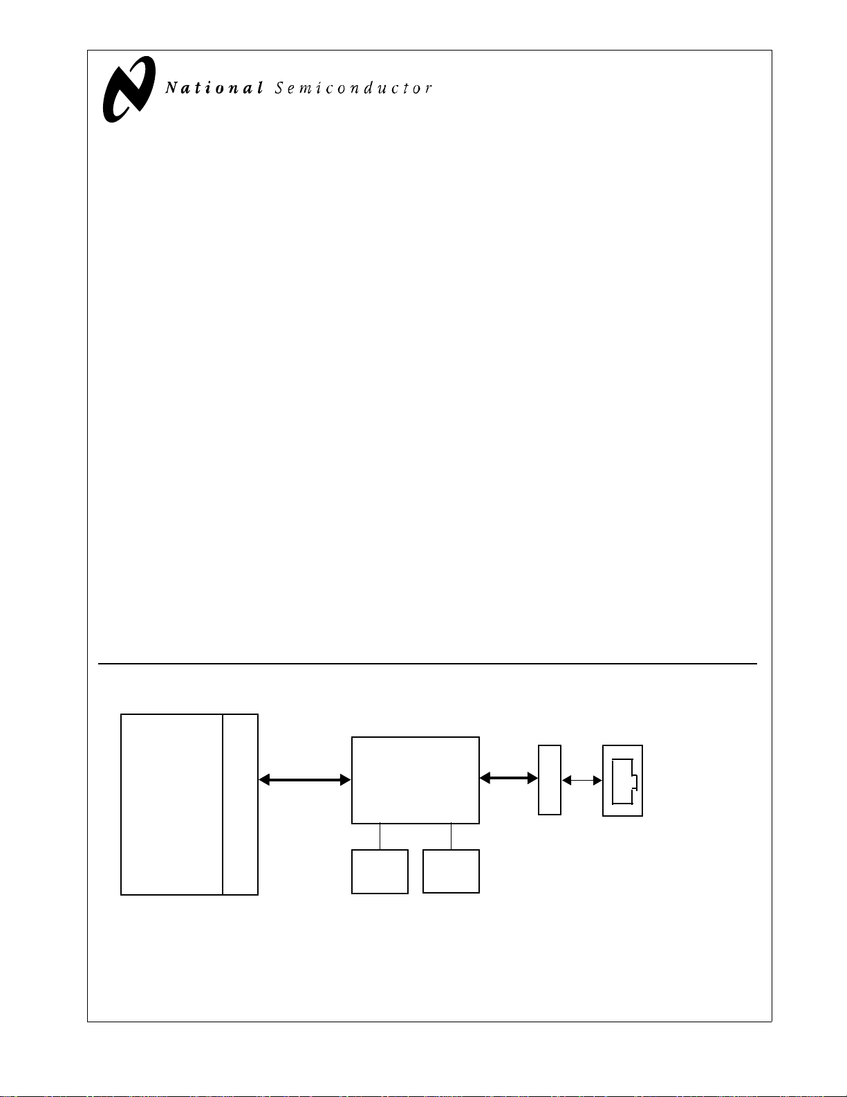
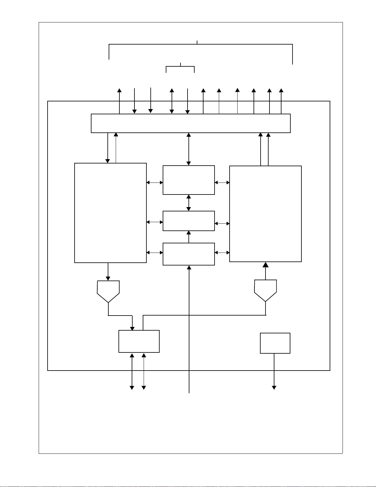
System Diagram
DP83848J
MPU/CPU
PHYTER® is a registered trademark of National Semiconductor Corporation.
© 2008 National Semiconductor Corporation
MII/RMII
Media Access Controlleroler
10/100 Ethernet
Transceiver
Clock
Source
Typical Ethernet Application
10BASE-T
Magnetics
Status
LED/s
www.national.com
RJ-45
or
100BASE-TX
MII/RMII
DP83848J
TX_CLK
TXD[3:0]
TX_DATA TX_CLK
10BASE-T &
100BASE-TX
Transmit
Block
SERIAL
MANAGEMENT
TX_EN
MDIO
MII/RMII INTERFACE
MII
Registers
Auto-Negotiation
State Machine
MDC
COL
CRS/CRS_DV
RX_ER
RX_DV
RX_CLK
10BASE-T &
100BASE-TX
Receive
Block
RXD[3:0]
RX_CLK
RX_DATA
Clock
Generation
DAC
Auto-MDIX
ADC
LED
Driver
TD±
Figure 1. DP83848J Functional Block Diagram
LEDS
RD±
REFERENCE CLOCK
www.national.com 2

Table of Contents
1.0 Pin Descriptions . . . . . . . . . . . . . . . . . . . . . . . . . . . . . . . . . . . . . . . . . . . . . . . . . 9
1.1 Serial Management Interface . . . . . . . . . . . . . . . . . . . . . . . . . . . . . . . . . . . . . . . . . . . . . . .9
1.2 MAC Data Interface . . . . . . . . . . . . . . . . . . . . . . . . . . . . . . . . . . . . . . . . . . . . . . . . . . . . . .9
1.3 Clock Interface . . . . . . . . . . . . . . . . . . . . . . . . . . . . . . . . . . . . . . . . . . . . . . . . . . . . . . . . .10
1.4 LED Interface . . . . . . . . . . . . . . . . . . . . . . . . . . . . . . . . . . . . . . . . . . . . . . . . . . . . . . . . . .11
1.5 Reset . . . . . . . . . . . . . . . . . . . . . . . . . . . . . . . . . . . . . . . . . . . . . . . . . . . . . . . . . . . . . . . .11
1.6 Strap Options . . . . . . . . . . . . . . . . . . . . . . . . . . . . . . . . . . . . . . . . . . . . . . . . . . . . . . . . . .11
1.7 10 Mb/s and 100 Mb/s PMD Interface . . . . . . . . . . . . . . . . . . . . . . . . . . . . . . . . . . . . . . .13
1.8 Special Connections . . . . . . . . . . . . . . . . . . . . . . . . . . . . . . . . . . . . . . . . . . . . . . . . . . . . .13
1.9 Power Supply Pins . . . . . . . . . . . . . . . . . . . . . . . . . . . . . . . . . . . . . . . . . . . . . . . . . . . . . .13
1.10 Package Pin Assignments . . . . . . . . . . . . . . . . . . . . . . . . . . . . . . . . . . . . . . . . . . . . . . .14
2.0 Configuration . . . . . . . . . . . . . . . . . . . . . . . . . . . . . . . . . . . . . . . . . . . . . . . . . . 15
2.1 Auto-Negotiation . . . . . . . . . . . . . . . . . . . . . . . . . . . . . . . . . . . . . . . . . . . . . . . . . . . . . . . .15
2.1.1 Auto-Negotiation Pin Control . . . . . . . . . . . . . . . . . . . . . . . . . . . . . . . . . . . . . . . . . . . . . . . . . 15
2.1.2 Auto-Negotiation Register Control . . . . . . . . . . . . . . . . . . . . . . . . . . . . . . . . . . . . . . . . . . . . . 15
2.1.3 Auto-Negotiation Parallel Detection . . . . . . . . . . . . . . . . . . . . . . . . . . . . . . . . . . . . . . . . . . . . 16
2.1.4 Auto-Negotiation Restart . . . . . . . . . . . . . . . . . . . . . . . . . . . . . . . . . . . . . . . . . . . . . . . . . . . . 16
2.1.5 Auto-Negotiation Complete Time . . . . . . . . . . . . . . . . . . . . . . . . . . . . . . . . . . . . . . . . . . . . . . 16
2.2 Auto-MDIX . . . . . . . . . . . . . . . . . . . . . . . . . . . . . . . . . . . . . . . . . . . . . . . . . . . . . . . . . . . .16
2.3 PHY Address . . . . . . . . . . . . . . . . . . . . . . . . . . . . . . . . . . . . . . . . . . . . . . . . . . . . . . . . . .17
2.3.1 MII Isolate Mode . . . . . . . . . . . . . . . . . . . . . . . . . . . . . . . . . . . . . . . . . . . . . . . . . . . . . . . . . . 17
2.4 LED Interface . . . . . . . . . . . . . . . . . . . . . . . . . . . . . . . . . . . . . . . . . . . . . . . . . . . . . . . . . .18
2.4.1 LED . . . . . . . . . . . . . . . . . . . . . . . . . . . . . . . . . . . . . . . . . . . . . . . . . . . . . . . . . . . . . . . . . . . . 18
2.4.2 LED Direct Control . . . . . . . . . . . . . . . . . . . . . . . . . . . . . . . . . . . . . . . . . . . . . . . . . . . . . . . . . 18
2.5 Half Duplex vs. Full Duplex . . . . . . . . . . . . . . . . . . . . . . . . . . . . . . . . . . . . . . . . . . . . . . .19
2.6 Internal Loopback . . . . . . . . . . . . . . . . . . . . . . . . . . . . . . . . . . . . . . . . . . . . . . . . . . . . . . .19
2.7 BIST . . . . . . . . . . . . . . . . . . . . . . . . . . . . . . . . . . . . . . . . . . . . . . . . . . . . . . . . . . . . . . . . .19
3.0 Functional Description. . . . . . . . . . . . . . . . . . . . . . . . . . . . . . . . . . . . . . . . . . . 20
3.1 MII Interface . . . . . . . . . . . . . . . . . . . . . . . . . . . . . . . . . . . . . . . . . . . . . . . . . . . . . . . . . . .20
3.1.1 Nibble-wide MII Data Interface . . . . . . . . . . . . . . . . . . . . . . . . . . . . . . . . . . . . . . . . . . . . . . . . 20
3.1.2 Collision Detect . . . . . . . . . . . . . . . . . . . . . . . . . . . . . . . . . . . . . . . . . . . . . . . . . . . . . . . . . . . 20
3.1.3 Carrier Sense . . . . . . . . . . . . . . . . . . . . . . . . . . . . . . . . . . . . . . . . . . . . . . . . . . . . . . . . . . . . . 20
3.2 Reduced MII Interface . . . . . . . . . . . . . . . . . . . . . . . . . . . . . . . . . . . . . . . . . . . . . . . . . . .20
3.3 802.3u MII Serial Management Interface . . . . . . . . . . . . . . . . . . . . . . . . . . . . . . . . . . . . .21
3.3.1 Serial Management Register Access . . . . . . . . . . . . . . . . . . . . . . . . . . . . . . . . . . . . . . . . . . . 21
3.3.2 Serial Management Access Protocol . . . . . . . . . . . . . . . . . . . . . . . . . . . . . . . . . . . . . . . . . . . 21
3.3.3 Serial Management Preamble Suppression . . . . . . . . . . . . . . . . . . . . . . . . . . . . . . . . . . . . . 22
4.0 Architecture. . . . . . . . . . . . . . . . . . . . . . . . . . . . . . . . . . . . . . . . . . . . . . . . . . . . 23
4.1 100BASE-TX TRANSMITTER . . . . . . . . . . . . . . . . . . . . . . . . . . . . . . . . . . . . . . . . . . . . .23
4.1.1 Code-group Encoding and Injection . . . . . . . . . . . . . . . . . . . . . . . . . . . . . . . . . . . . . . . . . . . . 25
4.1.2 Scrambler . . . . . . . . . . . . . . . . . . . . . . . . . . . . . . . . . . . . . . . . . . . . . . . . . . . . . . . . . . . . . . . . 25
4.1.3 NRZ to NRZI Encoder . . . . . . . . . . . . . . . . . . . . . . . . . . . . . . . . . . . . . . . . . . . . . . . . . . . . . . 25
4.1.4 Binary to MLT-3 Convertor . . . . . . . . . . . . . . . . . . . . . . . . . . . . . . . . . . . . . . . . . . . . . . . . . . . 25
4.2 100BASE-TX RECEIVER . . . . . . . . . . . . . . . . . . . . . . . . . . . . . . . . . . . . . . . . . . . . . . . . .25
4.2.1 Analog Front End . . . . . . . . . . . . . . . . . . . . . . . . . . . . . . . . . . . . . . . . . . . . . . . . . . . . . . . . . . 25
4.2.2 Digital Signal Processor . . . . . . . . . . . . . . . . . . . . . . . . . . . . . . . . . . . . . . . . . . . . . . . . . . . . . 25
4.2.2.1 Digital Adaptive Equalization and Gain Control . . . . . . . . . . . . . . . . . . . . . . . . . . . . . . 27
4.2.2.2 Base Line Wander Compensation . . . . . . . . . . . . . . . . . . . . . . . . . . . . . . . . . . . . . . . . 28
4.2.3 Signal Detect . . . . . . . . . . . . . . . . . . . . . . . . . . . . . . . . . . . . . . . . . . . . . . . . . . . . . . . . . . . . . 28
4.2.4 MLT-3 to NRZI Decoder . . . . . . . . . . . . . . . . . . . . . . . . . . . . . . . . . . . . . . . . . . . . . . . . . . . . . 28
4.2.5 NRZI to NRZ . . . . . . . . . . . . . . . . . . . . . . . . . . . . . . . . . . . . . . . . . . . . . . . . . . . . . . . . . . . . . 28
4.2.6 Serial to Parallel . . . . . . . . . . . . . . . . . . . . . . . . . . . . . . . . . . . . . . . . . . . . . . . . . . . . . . . . . . . 28
4.2.7 Descrambler . . . . . . . . . . . . . . . . . . . . . . . . . . . . . . . . . . . . . . . . . . . . . . . . . . . . . . . . . . . . . . 29
4.2.8 Code-group Alignment . . . . . . . . . . . . . . . . . . . . . . . . . . . . . . . . . . . . . . . . . . . . . . . . . . . . . . 29
4.2.9 4B/5B Decoder . . . . . . . . . . . . . . . . . . . . . . . . . . . . . . . . . . . . . . . . . . . . . . . . . . . . . . . . . . . . 29
DP83848J
3 www.national.com

4.2.10 100BASE-TX Link Integrity Monitor . . . . . . . . . . . . . . . . . . . . . . . . . . . . . . . . . . . . . . . . . . .29
4.2.11 Bad SSD Detection . . . . . . . . . . . . . . . . . . . . . . . . . . . . . . . . . . . . . . . . . . . . . . . . . . . . . . . . 29
4.3 10BASE-T TRANSCEIVER MODULE . . . . . . . . . . . . . . . . . . . . . . . . . . . . . . . . . . . . . . 29
DP83848J
4.3.1 Operational Modes . . . . . . . . . . . . . . . . . . . . . . . . . . . . . . . . . . . . . . . . . . . . . . . . . . . . . . . . . 29
4.3.2 Smart Squelch . . . . . . . . . . . . . . . . . . . . . . . . . . . . . . . . . . . . . . . . . . . . . . . . . . . . . . . . . . . . 30
4.3.3 Collision Detection and SQE . . . . . . . . . . . . . . . . . . . . . . . . . . . . . . . . . . . . . . . . . . . . . . . . . 30
4.3.4 Carrier Sense . . . . . . . . . . . . . . . . . . . . . . . . . . . . . . . . . . . . . . . . . . . . . . . . . . . . . . . . . . . . . 30
4.3.5 Normal Link Pulse Detection/Generation . . . . . . . . . . . . . . . . . . . . . . . . . . . . . . . . . . . . . . . . 30
4.3.6 Jabber Function . . . . . . . . . . . . . . . . . . . . . . . . . . . . . . . . . . . . . . . . . . . . . . . . . . . . . . . . . . . 31
4.3.7 Automatic Link Polarity Detection and Correction . . . . . . . . . . . . . . . . . . . . . . . . . . . . . . . . . 31
4.3.8 Transmit and Receive Filtering . . . . . . . . . . . . . . . . . . . . . . . . . . . . . . . . . . . . . . . . . . . . . . . . 31
4.3.9 Transmitter . . . . . . . . . . . . . . . . . . . . . . . . . . . . . . . . . . . . . . . . . . . . . . . . . . . . . . . . . . . . . . . 31
4.3.10 Receiver . . . . . . . . . . . . . . . . . . . . . . . . . . . . . . . . . . . . . . . . . . . . . . . . . . . . . . . . . . . . . . . . 31
5.0 Design Guidelines. . . . . . . . . . . . . . . . . . . . . . . . . . . . . . . . . . . . . . . . . . . . . . . 32
5.1 TPI Network Circuit . . . . . . . . . . . . . . . . . . . . . . . . . . . . . . . . . . . . . . . . . . . . . . . . . . . . . 32
5.2 ESD Protection . . . . . . . . . . . . . . . . . . . . . . . . . . . . . . . . . . . . . . . . . . . . . . . . . . . . . . . . 33
5.3 Clock In (X1) Recommendations . . . . . . . . . . . . . . . . . . . . . . . . . . . . . . . . . . . . . . . . . . 33
5.4 Power Feedback Circuit . . . . . . . . . . . . . . . . . . . . . . . . . . . . . . . . . . . . . . . . . . . . . . . . . 35
5.5 Power Down . . . . . . . . . . . . . . . . . . . . . . . . . . . . . . . . . . . . . . . . . . . . . . . . . . . . . . . . . . 35
5.6 Energy Detect Mode . . . . . . . . . . . . . . . . . . . . . . . . . . . . . . . . . . . . . . . . . . . . . . . . . . . . 35
6.0 Reset Operation. . . . . . . . . . . . . . . . . . . . . . . . . . . . . . . . . . . . . . . . . . . . . . . . . 35
6.1 Hardware Reset . . . . . . . . . . . . . . . . . . . . . . . . . . . . . . . . . . . . . . . . . . . . . . . . . . . . . . . 35
6.2 Software Reset . . . . . . . . . . . . . . . . . . . . . . . . . . . . . . . . . . . . . . . . . . . . . . . . . . . . . . . . 35
7.0 Register Block . . . . . . . . . . . . . . . . . . . . . . . . . . . . . . . . . . . . . . . . . . . . . . . . . 36
7.1 Register Definition . . . . . . . . . . . . . . . . . . . . . . . . . . . . . . . . . . . . . . . . . . . . . . . . . . . . . . 39
7.1.1 Basic Mode Control Register (BMCR) . . . . . . . . . . . . . . . . . . . . . . . . . . . . . . . . . . . . . . . . . . 40
7.1.2 Basic Mode Status Register (BMSR) . . . . . . . . . . . . . . . . . . . . . . . . . . . . . . . . . . . . . . . . . . . 42
7.1.3 PHY Identifier Register #1 (PHYIDR1) . . . . . . . . . . . . . . . . . . . . . . . . . . . . . . . . . . . . . . . . . . 43
7.1.4 PHY Identifier Register #2 (PHYIDR2) . . . . . . . . . . . . . . . . . . . . . . . . . . . . . . . . . . . . . . . . . . 43
7.1.5 Auto-Negotiation Advertisement Register (ANAR) . . . . . . . . . . . . . . . . . . . . . . . . . . . . . . . . . 43
7.1.6 Auto-Negotiation Link Partner Ability Register (ANLPAR) (BASE Page) . . . . . . . . . . . . . . . . 45
7.1.7 Auto-Negotiation Link Partner Ability Register (ANLPAR) (Next Page) . . . . . . . . . . . . . . . . . 46
7.1.8 Auto-Negotiate Expansion Register (ANER) . . . . . . . . . . . . . . . . . . . . . . . . . . . . . . . . . . . . . 46
7.1.9 Auto-Negotiation Next Page Transmit Register (ANNPTR) . . . . . . . . . . . . . . . . . . . . . . . . . . 47
7.2 Extended Registers . . . . . . . . . . . . . . . . . . . . . . . . . . . . . . . . . . . . . . . . . . . . . . . . . . . . . 48
7.2.1 PHY Status Register (PHYSTS) . . . . . . . . . . . . . . . . . . . . . . . . . . . . . . . . . . . . . . . . . . . . . . .48
7.2.2 False Carrier Sense Counter Register (FCSCR) . . . . . . . . . . . . . . . . . . . . . . . . . . . . . . . . . . 50
7.2.3 Receiver Error Counter Register (RECR) . . . . . . . . . . . . . . . . . . . . . . . . . . . . . . . . . . . . . . . . 50
7.2.4 100 Mb/s PCS Configuration and Status Register (PCSR) . . . . . . . . . . . . . . . . . . . . . . . . . . 51
7.2.5 RMII and Bypass Register (RBR) . . . . . . . . . . . . . . . . . . . . . . . . . . . . . . . . . . . . . . . . . . . . . .52
7.2.6 LED Direct Control Register (LEDCR) . . . . . . . . . . . . . . . . . . . . . . . . . . . . . . . . . . . . . . . . . . 53
7.2.7 PHY Control Register (PHYCR) . . . . . . . . . . . . . . . . . . . . . . . . . . . . . . . . . . . . . . . . . . . . . . .54
7.2.8 10Base-T Status/Control Register (10BTSCR) . . . . . . . . . . . . . . . . . . . . . . . . . . . . . . . . . . . 56
7.2.9 CD Test and BIST Extensions Register (CDCTRL1) . . . . . . . . . . . . . . . . . . . . . . . . . . . . . . . 57
7.2.10 Energy Detect Control (EDCR) . . . . . . . . . . . . . . . . . . . . . . . . . . . . . . . . . . . . . . . . . . . . . . . 58
8.0 Electrical Specifications . . . . . . . . . . . . . . . . . . . . . . . . . . . . . . . . . . . . . . . . . . 59
8.1 DC Specs . . . . . . . . . . . . . . . . . . . . . . . . . . . . . . . . . . . . . . . . . . . . . . . . . . . . . . . . . . . . 59
8.2 AC Specs . . . . . . . . . . . . . . . . . . . . . . . . . . . . . . . . . . . . . . . . . . . . . . . . . . . . . . . . . . . . 61
8.2.1 Power Up Timing . . . . . . . . . . . . . . . . . . . . . . . . . . . . . . . . . . . . . . . . . . . . . . . . . . . . . . . . . . 61
8.2.2 Reset Timing . . . . . . . . . . . . . . . . . . . . . . . . . . . . . . . . . . . . . . . . . . . . . . . . . . . . . . . . . . . . . 62
8.2.3 MII Serial Management Timing . . . . . . . . . . . . . . . . . . . . . . . . . . . . . . . . . . . . . . . . . . . . . . . . 63
8.2.4 100 Mb/s MII Transmit Timing . . . . . . . . . . . . . . . . . . . . . . . . . . . . . . . . . . . . . . . . . . . . . . . . 63
8.2.5 100 Mb/s MII Receive Timing . . . . . . . . . . . . . . . . . . . . . . . . . . . . . . . . . . . . . . . . . . . . . . . . 64
8.2.6 100BASE-TX Transmit Packet Latency Timing . . . . . . . . . . . . . . . . . . . . . . . . . . . . . . . . . . . 64
8.2.7 100BASE-TX Transmit Packet Deassertion Timing . . . . . . . . . . . . . . . . . . . . . . . . . . . . . . . . 65
8.2.8 100BASE-TX Transmit Timing (tR/F & Jitter) . . . . . . . . . . . . . . . . . . . . . . . . . . . . . . . . . . . . . 66
8.2.9 100BASE-TX Receive Packet Latency Timing . . . . . . . . . . . . . . . . . . . . . . . . . . . . . . . . . . . 67
8.2.10 100BASE-TX Receive Packet Deassertion Timing . . . . . . . . . . . . . . . . . . . . . . . . . . . . . . . 67
8.2.11 10 Mb/s MII Transmit Timing . . . . . . . . . . . . . . . . . . . . . . . . . . . . . . . . . . . . . . . . . . . . . . . . 68
8.2.12 10 Mb/s MII Receive Timing . . . . . . . . . . . . . . . . . . . . . . . . . . . . . . . . . . . . . . . . . . . . . . . . 68
www.national.com 4

8.2.13 10BASE-T Transmit Timing (Start of Packet) . . . . . . . . . . . . . . . . . . . . . . . . . . . . . . . . . . . 69
8.2.14 10BASE-T Transmit Timing (End of Packet) . . . . . . . . . . . . . . . . . . . . . . . . . . . . . . . . . . . . 69
8.2.15 10BASE-T Receive Timing (Start of Packet) . . . . . . . . . . . . . . . . . . . . . . . . . . . . . . . . . . . . 70
8.2.16 10BASE-T Receive Timing (End of Packet) . . . . . . . . . . . . . . . . . . . . . . . . . . . . . . . . . . . . . 70
8.2.17 10 Mb/s Heartbeat Timing . . . . . . . . . . . . . . . . . . . . . . . . . . . . . . . . . . . . . . . . . . . . . . . . . . 71
8.2.18 10 Mb/s Jabber Timing . . . . . . . . . . . . . . . . . . . . . . . . . . . . . . . . . . . . . . . . . . . . . . . . . . . . 71
8.2.19 10BASE-T Normal Link Pulse Timing . . . . . . . . . . . . . . . . . . . . . . . . . . . . . . . . . . . . . . . . . 72
8.2.20 Auto-Negotiation Fast Link Pulse (FLP) Timing . . . . . . . . . . . . . . . . . . . . . . . . . . . . . . . . . . 72
8.2.21 100BASE-TX Signal Detect Timing . . . . . . . . . . . . . . . . . . . . . . . . . . . . . . . . . . . . . . . . . . 73
8.2.22 100 Mb/s Internal Loopback Timing . . . . . . . . . . . . . . . . . . . . . . . . . . . . . . . . . . . . . . . . . . 73
8.2.23 10 Mb/s Internal Loopback Timing . . . . . . . . . . . . . . . . . . . . . . . . . . . . . . . . . . . . . . . . . . . 74
8.2.24 RMII Transmit Timing . . . . . . . . . . . . . . . . . . . . . . . . . . . . . . . . . . . . . . . . . . . . . . . . . . . . . . 75
8.2.25 RMII Receive Timing . . . . . . . . . . . . . . . . . . . . . . . . . . . . . . . . . . . . . . . . . . . . . . . . . . . . . . 76
8.2.26 Isolation Timing . . . . . . . . . . . . . . . . . . . . . . . . . . . . . . . . . . . . . . . . . . . . . . . . . . . . . . . . . . 77
8.2.27 100 Mb/s X1 to TX_CLK Timing . . . . . . . . . . . . . . . . . . . . . . . . . . . . . . . . . . . . . . . . . . . . . 77
DP83848J
5 www.national.com

List of Figures
DP83848J
Figure 1. DP83848J Functional Block Diagram . . . . . . . . . . . . . . . . . . . . . . . . . . . . . . . . . . . . . . . . . . . 2
Figure 2. PHYAD Strapping Example . . . . . . . . . . . . . . . . . . . . . . . . . . . . . . . . . . . . . . . . . . . . . . . . . 17
Figure 3. AN Strapping and LED Loading Example . . . . . . . . . . . . . . . . . . . . . . . . . . . . . . . . . . . . . . . 18
Figure 4. Typical MDC/MDIO Read Operation . . . . . . . . . . . . . . . . . . . . . . . . . . . . . . . . . . . . . . . . . . 22
Figure 5. Typical MDC/MDIO Write Operation . . . . . . . . . . . . . . . . . . . . . . . . . . . . . . . . . . . . . . . . . . . 22
Figure 6. 100BASE-TX Transmit Block Diagram . . . . . . . . . . . . . . . . . . . . . . . . . . . . . . . . . . . . . . . . . 23
Figure 7. 100BASE-TX Receive Block Diagram . . . . . . . . . . . . . . . . . . . . . . . . . . . . . . . . . . . . . . . . . 26
Figure 8. EIA/TIA Attenuation vs. Frequency for 0, 50, 100, 130 & 150 meters of CAT 5 cable . . . . . 27
Figure 9. 100BASE-TX BLW Event . . . . . . . . . . . . . . . . . . . . . . . . . . . . . . . . . . . . . . . . . . . . . . . . . . . 28
Figure 10. 10BASE-T Twisted Pair Smart Squelch Operation . . . . . . . . . . . . . . . . . . . . . . . . . . . . . . . 30
Figure 11. 10/100 Mb/s Twisted Pair Interface . . . . . . . . . . . . . . . . . . . . . . . . . . . . . . . . . . . . . . . . . . 32
Figure 12. Crystal Oscillator Circuit . . . . . . . . . . . . . . . . . . . . . . . . . . . . . . . . . . . . . . . . . . . . . . . . . . . 33
Figure 13. Power Feedback Connection . . . . . . . . . . . . . . . . . . . . . . . . . . . . . . . . . . . . . . . . . . . . . . . 35
www.national.com 6

List of Tables
Table 1. Auto-Negotiation Modes in DP83848J . . . . . . . . . . . . . . . . . . . . . . . . . . . . . . . . . . . . . . . . . . 15
Table 2. PHY Address Mapping . . . . . . . . . . . . . . . . . . . . . . . . . . . . . . . . . . . . . . . . . . . . . . . . . . . . . . 17
Table 3. LED Mode Select for DP83848J . . . . . . . . . . . . . . . . . . . . . . . . . . . . . . . . . . . . . . . . . . . . . . . 18
Table 4. Supported packet sizes at +/-50ppm +/-100ppm for each clock . . . . . . . . . . . . . . . . . . . . . . 21
Table 5. Typical MDIO Frame Format . . . . . . . . . . . . . . . . . . . . . . . . . . . . . . . . . . . . . . . . . . . . . . . . . 21
Table 6. 4B5B Code-Group Encoding/Decoding . . . . . . . . . . . . . . . . . . . . . . . . . . . . . . . . . . . . . . . . . 24
Table 7. 25 MHz Oscillator Specification . . . . . . . . . . . . . . . . . . . . . . . . . . . . . . . . . . . . . . . . . . . . . . . 33
Table 8. 50 MHz Oscillator Specification . . . . . . . . . . . . . . . . . . . . . . . . . . . . . . . . . . . . . . . . . . . . . . . 34
Table 9. 25 MHz Crystal Specification . . . . . . . . . . . . . . . . . . . . . . . . . . . . . . . . . . . . . . . . . . . . . . . . . 34
Table 10. Register Map . . . . . . . . . . . . . . . . . . . . . . . . . . . . . . . . . . . . . . . . . . . . . . . . . . . . . . . . . . . . 36
Table 11. Register Table . . . . . . . . . . . . . . . . . . . . . . . . . . . . . . . . . . . . . . . . . . . . . . . . . . . . . . . . . . . 37
Table 12. Basic Mode Control Register (BMCR), address 0x00 . . . . . . . . . . . . . . . . . . . . . . . . . . . . . 40
Table 13. Basic Mode Status Register (BMSR), address 0x01 . . . . . . . . . . . . . . . . . . . . . . . . . . . . . . 42
Table 14. PHY Identifier Register #1 (PHYIDR1), address 0x02 . . . . . . . . . . . . . . . . . . . . . . . . . . . . . 43
Table 15. PHY Identifier Register #2 (PHYIDR2), address 0x03 . . . . . . . . . . . . . . . . . . . . . . . . . . . . . 43
Table 16. Negotiation Advertisement Register (ANAR), address 0x04 . . . . . . . . . . . . . . . . . . . . . . . . 43
Table 17. Auto-Negotiation Link Partner Ability Register (ANLPAR) (BASE Page), address 0x05 . . . 45
Table 18. Auto-Negotiation Link Partner Ability Register (ANLPAR) (Next Page), address 0x05 . . . . 46
Table 19. Auto-Negotiate Expansion Register (ANER), address 0x06 . . . . . . . . . . . . . . . . . . . . . . . . 46
Table 20. Auto-Negotiation Next Page Transmit Register (ANNPTR), address 0x07 . . . . . . . . . . . . . 47
Table 21. PHY Status Register (PHYSTS), address 0x10 . . . . . . . . . . . . . . . . . . . . . . . . . . . . . . . . . . 48
Table 22. False Carrier Sense Counter Register (FCSCR), address 0x14 . . . . . . . . . . . . . . . . . . . . . 50
Table 23. Receiver Error Counter Register (RECR), address 0x15 . . . . . . . . . . . . . . . . . . . . . . . . . . . 50
Table 24. 100 Mb/s PCS Configuration and Status Register (PCSR), address 0x16 . . . . . . . . . . . . . 51
Table 25. RMII and Bypass Register (RBR), addresses 0x17 . . . . . . . . . . . . . . . . . . . . . . . . . . . . . . . 52
Table 26. LED Direct Control Register (LEDCR), address 0x18 . . . . . . . . . . . . . . . . . . . . . . . . . . . . . 53
Table 27. PHY Control Register (PHYCR), address 0x19 . . . . . . . . . . . . . . . . . . . . . . . . . . . . . . . . . . 54
Table 28. 10Base-T Status/Control Register (10BTSCR), address 0x1A . . . . . . . . . . . . . . . . . . . . . . 56
Table 29. CD Test and BIST Extensions Register (CDCTRL1), address 0x1B . . . . . . . . . . . . . . . . . . 57
Table 30. Energy Detect Control (EDCR), address 0x1D . . . . . . . . . . . . . . . . . . . . . . . . . . . . . . . . . . 58
DP83848J
7 www.national.com

Pin Layout for DP83848J
DP83848J
RXD_2/PHYAD3
RXD_3/PHYAD4
RXD_0/PHYAD1
RXD_1/PHYAD2
RX_ER/MDIX_EN
COL/PHYAD0
CRS/CRS_DV/LED_CFG
RX_DV/MII_MODE
RX_CLK
31
32
33
PFBIN2
30
DGND
29
X1
28
X2
27
IOVDD33
26
MDC
25
MDIO
24
RESET_N
23
LED_LINK/AN0
19
PFBOUT
22
LED_SPEED/AN1
21
20
RBIAS
DAP
18
AVDD33
IOVDD33
TX_CLK
TX_EN
TXD_0
TXD_1
TXD_2
TXD_3
RESERVED
RESERVED
RESERVED
IOGND
34
35
36
37
38
39
40
1
2
3
4
5
6
7
8
9
10
11
RD -
DP83848J
14
13
12
TD -
AGND
RD +
17
16
15
AGND
PFBIN1
TD +
Note: Die Attached Pad (DAP) provides thermal dissipation, connection to GND plane optional.
Top View
Order Number DP83848J
NS Package Number NSQAU040
www.national.com 8

1.0 Pin Descriptions
The DP83848J pins are classified into the following interface categories (each interface is described in the sections
that follow):
— Serial Management Interface
— MAC Data Interface
— Clock Interface
— LED Interface
—Reset
— Strap Options
— 10/100 Mb/s PMD Interface
— Special Connect Pins
— Power and Ground pins
1.1 SERIAL MANAGEMENT INTERFACE
Signal Name Type Pin # Description
MDC I 25 MANAGEMENT DATA CLOCK: Synchronous clock to the MDIO
MDIO I/O 24 MANAGEMENT DATA I/O: Bi-directional management instruc-
Note: Strapping pin option. Please see Section 1.6 for strap
definitions.
All DP83848J signal pins are I/O cells regardless of the
particular use. The definitions below define the functionality
of the I/O cells for each pin.
Type: I Input
Type: O Output
Type: I/O Input/Output
Type: PD,PU Internal Pulldown/Pullup
Type: S Strapping Pin (All strap pins have weak in-
ternal pull-ups or pull-downs. If the default
strap value is needed to be changed then an
external 2.2 kΩ resistor should be used.
Please see Section 1.6 for details.)
management data input/output serial interface which may be
asynchronous to transmit and receive clocks. The maximum clock
rate is 25 MHz with no minimum clock rate.
tion/data signal that may be sourced by the station management
entity or the PHY. This pin requires a 1.5 kΩ pullup resistor.
DP83848J
1.2 MAC DATA INTERFACE
Signal Name Type Pin # Description
TX_CLK O 2 MII TRANSMIT CLOCK: 25 MHz Transmit clock output in 100
TX_EN I, PD 3 MII TRANSMIT ENABLE: Active high input indicates the pres-
TXD_0
TXD_1
TXD_2
TXD_3
RX_CLK O 31 MII RECEIVE CLOCK: Provides the 25 MHz recovered receive
RX_DV O, PD 32 MII RECEIVE DATA VALID: Asserted high to indicate that valid
I
I, PD
4
5
6
7
Mb/s mode or 2.5 MHz in 10 Mb/s mode derived from the 25 MHz
reference clock.
Unused in RMII mode. The device uses the X1 reference clock input as the 50 MHz reference for both transmit and receive.
ence of valid data inputs on TXD[3:0].
RMII TRANSMIT ENABLE: Active high input indicates the presence of valid data on TXD[1:0].
MII TRANSMIT DATA: Transmit data MII input pins, TXD[3:0],
that accept data synchronous to the TX_CLK (2.5 MHz in 10 Mb/s
mode or 25 MHz in 100 Mb/s mode).
RMII TRANSMIT DATA: Transmit data RMII input pins, TXD[1:0],
that accept data synchronous to the 50 MHz reference clock.
clocks for 100 Mb/s mode and 2.5 MHz for 10 Mb/s mode.
Unused in RMII mode. The device uses the X1 reference clock input as the 50 MHz reference for both transmit and receive.
data is present on the corresponding RXD[3:0].
RMII Synchronous Receive Data Valid: This signal provides the
RMII Receive Data Valid indication independent of Carrier Sense.
9 www.national.com

Signal Name Type Pin # Description
RX_ER S, O, PU 34 MII RECEIVE ERROR: Asserted high synchronously to RX_CLK
to indicate that an invalid symbol has been detected within a re-
DP83848J
RXD_0
RXD_1
RXD_2
RXD_3
CRS/CRS_DV S, O, PU 33 MII CARRIER SENSE: Asserted high to indicate the receive me-
COL S, O, PU 35 MII COLLISION DETECT: Asserted high to indicate detection of
S, O, PD 36
37
38
39
ceived packet in 100 Mb/s mode.
RMII RECEIVE ERROR: Assert high synchronously to X1 whenever it detects a media error and RX_DV is asserted in 100 Mb/s
mode.
This pin is not required to be used by a MAC, in either MII or RMII
mode, since the Phy is required to corrupt data on a receive error.
MII RECEIVE DATA: Nibble wide receive data signals driven synchronously to the RX_CLK, 25 MHz for 100 Mb/s mode, 2.5 MHz
for 10 Mb/s mode). RXD[3:0] signals contain valid data when
RX_DV is asserted.
RMII RECEIVE DATA: 2-bits receive data signals, RXD[1:0], driven synchronously to the X1 clock, 50 MHz.
dium is non-idle.
RMII CARRIER SENSE/RECEIVE DATA VALID: This signal
combines the RMII Carrier and Receive Data Valid indications.
For a detailed description of this signal, see the RMII Specification.
a collision condition (simultaneous transmit and receive activity)
in 10 Mb/s and 100 Mb/s Half Duplex Modes.
While in 10BASE-T Half Duplex mode with heartbeat enabled this
pin is also asserted for a duration of approximately 1µs at the end
of transmission to indicate heartbeat (SQE test).
In Full Duplex Mode, for 10 Mb/s or 100 Mb/s operation, this signal is always logic 0. There is no heartbeat function during 10
Mb/s full duplex operation.
RMII COLLISION DETECT: Per the RMII Specification, no COL
signal is required. The MAC will recover CRS from the CRS_DV
signal and use that along with its TX_EN signal to determine collision.
1.3 CLOCK INTERFACE
Signal Name Type Pin # Description
X1 I 28 CRYSTAL/OSCILLATOR INPUT: This pin is the primary clock
reference input for the DP83848J and must be connected to a 25
MHz 0.005% (+
ther an external crystal resonator connected across pins X1 and
X2, or an external CMOS-level oscillator source connected to pin
X1 only.
RMII REFERENCE CLOCK: This pin is the primary clock reference input for the RMII mode and must be connected to a 50 MHz
0.005% (+50 ppm) CMOS-level oscillator source.
X2 O 27 CRYSTAL OUTPUT: This pin is the primary clock reference out-
put to connect to an external 25 MHz crystal resonator device.
This pin must be left unconnected if an external CMOS oscillator
clock source is used.
50 ppm) clock source. The DP83848J supports ei-
www.national.com 10

1.4 LED INTERFACE
See Table 3 for LED Mode Selection.
Signal Name Type Pin # Description
LED_LINK S, O, PU 22 LINK LED: In Mode 1, this pin indicates the status of the LINK.
The LED will be ON when Link is good.
LINK/ACT LED: In Mode 2, this pin indicates transmit and receive
activity in addition to the status of the Link. The LED will be ON
when Link is good. It will blink when the transmitter or receiver is
active.
LED_SPEED S, O, PU 21 SPEED LED: This LED is ON when DP83848J is in 100Mb/s and
OFF when DP83848J is in 10Mb/s. Functionality of this LED is independent of the mode selected.
1.5 RESET
Signal Name Type Pin # Description
RESET_N I, PU 23 RESET: Active Low input that initializes or re-initializes the
DP83848J. Asserting this pin low for at least 1 µs will force a reset
process to occur. All internal registers will re-initialize to their default states as specified for each bit in the Register Block section.
All strap options are re-initialized as well.
DP83848J
1.6 STRAP OPTIONS
DP83848J uses many functional pins as strap options. The
values of these pins are sampled during reset and used to
strap the device into specific modes of operation. The strap
option pin assignments are defined below. The functional
pin name is indicated in parentheses.
Signal Name Type Pin # Description
PHYAD0 (COL)
PHYAD1 (RXD_0)
PHYAD2 (RXD_1)
PHYAD3 (RXD_2)
PHYAD4 (RXD_3)
S, O, PU
S, O, PD
35
36
37
38
39
PHY ADDRESS [4:0]: The DP83848J provides five PHY address
pins, the state of which are latched into the PHYCTRL register at
system Hardware-Reset.
The DP83848J supports PHY Address strapping values 0
(<00000>) through 31 (<11111>). A PHY Address of 0 puts the
part into the MII Isolate Mode. The MII isolate mode must be selected by strapping Phy Address 0; changing to Address 0 by register write will not put the Phy in the MII isolate mode. Please refer
to section 2.3 for additional information.
PHYAD0 pin has weak internal pull-up resistor.
PHYAD[4:1] pins have weak internal pull-down resistors.
A 2.2 kΩ resistor should be used for pull-down or pull-up to
change the default strap option. If the default option is
required, then there is no need for external pull-up or pull
down resistors. Since these pins may have alternate functions after reset is deasserted, they should not be connected directly to VCC or GND.
11 www.national.com
Signal Name Type Pin # Description
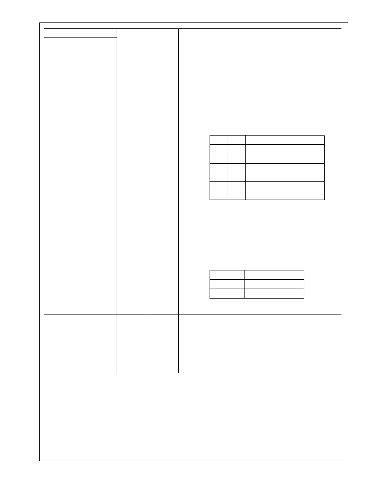
AN0 (LED_LINK)
AN1 (LED_SPEED)
DP83848J
S, O, PU
S, O, PU
22
21
These input pins control the advertised operating mode of the device according to the following table. The value on these pins are
set by connecting them to GND (0) or V
sistors. These pins should NEVER be connected directly to
GND or VCC.
The value set at this input is latched into the DP83848J at Hardware-Reset.
The float/pull-down status of these pins are latched into the Basic
Mode Control Register and the Auto_Negotiation Advertisement
Register during Hardware-Reset.
The default for DP83848J is 11 since these pins have an internal
pull-up.
AN1 AN0 Advertised Mode
0 0 10BASE-T, Half/Full-Duplex
0 1 100BASE-TX, Half/Full-Duplex
1 0 10BASE-T, Half-Duplex
100BASE-TX, Half-Duplex
1 1 10BASE-T, Half/Full-Duplex
100BASE-TX, Half/Full-Duplex
(1) through 2.2 kΩ re-
CC
MII_MODE (RX_DV) S, O, PD 32 MII MODE SELECT: This strapping option determines the oper-
LED_CFG (CRS/CRS_DV) S, O, PU 33 LED CONFIGURATION: This strapping option determines the
MDIX_EN (RX_ER) S, O, PU 34 MDIX ENABLE: Default is to enable MDIX. This strapping option
ating mode of the MAC Data Interface. Default operation (No pullup) will enable normal MII Mode of operation. Strapping
MII_MODE high will cause the device to be in RMII mode of operation. Since the pin includes an internal pull-down, the default value is 0.
The following table details the configuration:
MII_MODE MAC Interface Mode
0MII Mode
1 RMII Mode
mode of operation of the LED pins. Default is Mode 1. Mode 1 and
Mode 2 can be controlled via the strap option. All modes are configurable via register access.
SeeTable 3 for LED Mode Selection.
disables Auto-MDIX. An external pull-down will disable AutoMDIX mode.
www.national.com 12

1.7 10 MB/S AND 100 MB/S PMD INTERFACE
Signal Name Type Pin # Description
TD-, TD+ I/O 14, 15 Differential common driver transmit output (PMD Output Pair).
RD-, RD+ I/O 11, 12 Differential receive input (PMD Input Pair). These differential in-
These differential outputs are automatically configured to either
10BASE-T or 100BASE-TX signaling.
In Auto-MDIX mode of operation, this pair can be used as the Receive Input pair.
These pins require 3.3V bias for operation.
puts are automatically configured to accept either 100BASE-TX
or 10BASE-T signaling.
In Auto-MDIX mode of operation, this pair can be used as the
Transmit Output pair.
These pins require 3.3V bias for operation.
1.8 SPECIAL CONNECTIONS
Signal Name Type Pin # Description
RBIAS I 20 Bias Resistor Connection. A 4.87 kΩ 1% resistor should be con-
PFBOUT O 19 Power Feedback Output. Parallel caps, 10µ F (Tantalum pre-
PFBIN1
PFBIN2
RESERVED I/O 8,9,10 RESERVED: These pins must be left unconnected.
I16
30
nected from RBIAS to GND.
ferred) and 0.1µF, should be placed close to the PFBOUT. Con-
nect this pin to PFBIN1 (pin 16) and PFBIN2 (pin 30). See
Section 5.4 for proper placement pin.
Power Feedback Input. These pins are fed with power from
PFBOUT pin. A small capacitor of 0.1µF should be connected
close to each pin.
Note: Do not supply power to these pins other than from
PFBOUT.
DP83848J
1.9 POWER SUPPLY PINS
Signal Name Pin # Description
IOVDD33 1, 26 I/O 3.3V Supply
IOGND 40 I/O Ground
DGND 29 Digital Ground
AVDD33 18 Analog 3.3V Supply
AGND 13, 17 Analog Ground
13 www.national.com

1.10 PACKAGE PIN ASSIGNMENTS
DP83848J
NSQAU040
Pin #
1IO_VDD
2TX_CLK
3 TX_EN
4TXD_0
5TXD_1
6TXD_2
7TXD_3
8 RESERVED
9 RESERVED
10 RESERVED
11 RD-
12 RD+
13 AGND
14 TD -
15 TD +
16 PFBIN1
17 AGND
18 AVDD33
19 PFBOUT
20 RBIAS
21 LED_SPEED/AN1
22 LED_LINK/AN0
23 RESET_N
24 MDIO
25 MDC
26 IOVDD33
27 X2
28 X1
29 DGND
30 PFBIN2
31 RX_CLK
32 RX_DV/MII_MODE
33 CRS/CRS_DV/LED_CFG
34 RX_ER/MDIX_EN
35 COL/PHYAD0
36 RXD_0/PHYAD1
37 RXD_1/PHYAD2
38 RXD_2/PHYAD3
39 RXD_3/PHYAD4
40 IOGND
Pin Name
(DP83848J)
www.national.com 14

2.0 Configuration
This section includes information on the various configuration options available with the DP83848J. The configuration options described below include:
— Auto-Negotiation
— PHY Address and LED
— Half Duplex vs. Full Duplex
— Isolate mode
— Loopback mode
—BIST
2.1 AUTO-NEGOTIATION
The Auto-Negotiation function provides a mechanism for
exchanging configuration information between two ends of
a link segment and automatically selecting the highest performance mode of operation supported by both devices.
Fast Link Pulse (FLP) Bursts provide the signalling used to
communicate Auto-Negotiation abilities between two
devices at each end of a link segment. For further detail
regarding Auto-Negotiation, refer to Clause 28 of the IEEE
802.3u specification. The DP83848J supports four different
Ethernet protocols (10 Mb/s Half Duplex, 10 Mb/s Full
Duplex, 100 Mb/s Half Duplex, and 100 Mb/s Full Duplex),
so the inclusion of Auto-Negotiation ensures that the highest performance protocol will be selected based on the
advertised ability of the Link Partner. In DP83848J, the
Auto-Negotiation function can be controlled either by internal register access or by the use of AN0 and AN1 pins.
2.1.1 Auto-Negotiation Pin Control
The state of AN0 and AN1 pins determine the specific
mode advertised by the device as given in Table 1.. The
state of AN0 and AN1 pins, upon power-up/reset, determines the state of bits [8:5] of the ANAR register.
The Auto-Negotiation function selected at power-up or
reset can be changed at any time by writing to the Basic
Mode Control Register (BMCR) at address 0x00h
Table 1. Auto-Negotiation Modes in DP83848J
AN1 AN0 Advertised Mode
0 0 10BASE-T, Half/Full-Duplex
0 1 100BASE-TX, Half/Full-Duplex
1 0 10BASE-T, Half-Duplex
100BASE-TX, Half-Duplex
1 1 10BASE-T, Half/Full-Duplex
100BASE-TX, Half/Full-Duplex
DP83848J
2.1.2 Auto-Negotiation Register Control
When Auto-Negotiation is enabled, the DP83848J transmits the abilities programmed into the Auto-Negotiation
Advertisement register (ANAR) at address 04h via FLP
Bursts. Any combination of 10 Mb/s, 100 Mb/s, HalfDuplex, and Full Duplex modes may be selected.
Auto-Negotiation Priority Resolution:
— (1) 100BASE-TX Full Duplex (Highest Priority)
— (2) 100BASE-TX Half Duplex
— (3) 10BASE-T Full Duplex
— (4) 10BASE-T Half Duplex (Lowest Priority)
The Basic Mode Control Register (BMCR) at address 00h
provides control for enabling, disabling, and restarting the
Auto-Negotiation process. When Auto-Negotiation is disabled, the Speed Selection bit in the BMCR controls
switching between 10 Mb/s or 100 Mb/s operation, and the
Duplex Mode bit controls switching between full duplex
operation and half duplex operation. The Speed Selection
and Duplex Mode bits have no effect on the mode of operation when the Auto-Negotiation Enable bit is set.
The Link Speed can be examined through the PHY Status
Register (PHYSTS) at address 10h after a Link is
achieved.
The Basic Mode Status Register (BMSR) indicates the set
of available abilities for technology types, Auto-Negotiation
ability, and Extended Register Capability. These bits are
permanently set to indicate the full functionality of the
DP83848J (only the 100BASE-T4 bit is not set since the
DP83848J does not support that function).
The BMSR also provides status on:
— Completion of Auto-Negotiation
— Occurrence of a remote fault as advertised by the Link
Partner
— Establishment of a valid link
— Support for Management Frame Preamble suppression
The Auto-Negotiation Advertisement Register (ANAR)
indicates the Auto-Negotiation abilities to be advertised by
the DP83848J. All available abilities are transmitted by
default, but any ability can be suppressed by writing to the
ANAR. Updating the ANAR to suppress an ability is one
way for a management agent to change (restrict) the technology that is used.
The Auto-Negotiation Link Partner Ability Register
(ANLPAR) at address 05h is used to receive the base link
code word as well as all next page code words during the
negotiation. Furthermore, the ANLPAR will be updated to
either 0081h or 0021h for parallel detection to either 100
Mb/s or 10 Mb/s respectively.
The Auto-Negotiation Expansion Register (ANER) indicates additional Auto-Negotiation status. The ANER provides status on:
— Occurrence of a Parallel Detect Fault
— Next Page function support by the Link Partner
— Next page support function by DP83848J
— Reception of the current page that is exchanged by Auto-
Negotiation
— Auto-Negotiation support by the Link Partner
15 www.national.com

2.1.3 Auto-Negotiation Parallel Detection
The DP83848J supports the Parallel Detection function as
defined in the IEEE 802.3u specification. Parallel Detection requires both the 10 Mb/s and 100 Mb/s receivers to
DP83848J
monitor the receive signal and report link status to the
Auto-Negotiation function. Auto-Negotiation uses this
information to configure the correct technology in the
event that the Link Partner does not support Auto-Negotiation but is transmitting link signals that the 100BASE-TX
or 10BASE-T PMAs recognize as valid link signals.
If the DP83848J completes Auto-Negotiation as a result of
Parallel Detection, bit 5 or bit 7 within the ANLPAR register will be set to reflect the mode of operation present in
the Link Partner. Note that bits 4:0 of the ANLPAR will also
be set to 00001 based on a successful parallel detection
to indicate a valid 802.3 selector field. Software may
determine that negotiation completed via Parallel Detection by reading a zero in the Link Partner Auto-Negotiation
Able bit once the Auto-Negotiation Complete bit is set. If
configured for parallel detect mode and any condition
other than a single good link occurs then the parallel
detect fault bit will be set.
2.1.4 Auto-Negotiation Restart
Once Auto-Negotiation has completed, it may be restarted
at any time by setting bit 9 (Restart Auto-Negotiation) of
the BMCR to one. If the mode configured by a successful
Auto-Negotiation loses a valid link, then the Auto-Negotiation process will resume and attempt to determine the
configuration for the link. This function ensures that a valid
configuration is maintained if the cable becomes disconnected.
A renegotiation request from any entity, such as a management agent, will cause the DP83848J to halt any
transmit data and link pulse activity until the
break_link_timer expires (~1500 ms). Consequently, the
Link Partner will go into link fail and normal Auto-Negotiation resumes. The DP83848J will resume Auto-Negotiation after the break_link_timer has expired by issuing FLP
(Fast Link Pulse) bursts.
Auto-MDIX is enabled by default and can be configured
via strap or via PHYCR (0x19h) register, bits [15:14].
Neither Auto-Negotiation nor Auto-MDIX is required to be
enabled in forcing crossover of the MDI pairs. Forced
crossover can be achieved through the FORCE_MDIX bit,
bit 14 of PHYCR (0x19h) register.
Note: Auto-MDIX will not work in a forced mode of operation.
2.1.5 Auto-Negotiation Complete Time
Parallel detection and Auto-Negotiation take approximately 2-3 seconds to complete. In addition, Auto-Negotiation with next page should take approximately 2-3
seconds to complete, depending on the number of next
pages sent.
Refer to Clause 28 of the IEEE 802.3u standard for a full
description of the individual timers related to Auto-Negotiation.
2.2 AUTO-MDIX
When enabled, this function utilizes Auto-Negotiation to
determine the proper configuration for transmission and
reception of data and subsequently selects the appropriate MDI pair for MDI/MDIX operation. The function uses a
random seed to control switching of the crossover circuitry. This implementation complies with the corresponding IEEE 802.3 Auto-Negotiation and Crossover
Specifications.
www.national.com 16

2.3 PHY ADDRESS
The 5 PHY address inputs pins are shared with the
RXD[3:0] pins and COL pin as shown below.
Table 2. PHY Address Mapping
Pin # PHYAD Function RXD Function
35 PHYAD0 COL
36 PHYAD1 RXD_0
37 PHYAD2 RXD_1
38 PHYAD3 RXD_2
39 PHYAD4 RXD_3
The DP83848J can be set to respond to any of 32 possible
PHY addresses via strap pins. The information is latched
into the PHYCR register (address 19h, bits [4:0]) at device
power-up and hardware reset. The PHY Address pins are
shared with the RXD and COL pins. Each DP83848J or
port sharing an MDIO bus in a system must have a unique
physical address.
The DP83848J supports PHY Address strapping values 0
(<0 0 00 0 >) t h r o u g h 3 1 ( <11111 > ) . Strap pi n g PHY Address
0 puts the part into Isolate Mode. It should also be noted
that selecting PHY Address 0 via an MDIO write to PHYCR
will not put the device in Isolate Mode. See Section 2.3.1
for more information.
For further detail relating to the latch-in timing requirements
of the PHY Address pins, as well as the other hardware
configuration pins, refer to the Reset summary in
Section 6.0.
DP83848J
Since the PHYAD[0] pin has weak internal pull-up resistor
and PHYAD[4:1] pins have weak internal pull-down resistors, the default setting for the PHY address is 00001
(01h).
Refer to Figure 2 for an example of a PHYAD connection to
external components. In this example, the PHYAD strapping results in address 00011 (03h).
2.3.1 MII Isolate Mode
The DP83848J can be put into MII Isolate mode by writing
to bit 10 of the BMCR register or by strapping in Physical
Address 0. It should be noted that selecting Physical
Address 0 via an MDIO write to PHYCR will not put the
device in the MII isolate mode.
When in the MII isolate mode, the DP83848J does not
respond to packet data present at TXD[3:0], TX_EN inputs
and presents a high impedance on the TX_CLK, RX_CLK,
RX_DV, RX_ER, RXD[3:0], COL, and CRS outputs. When
in Isolate mode, the DP83848J will continue to respond to
all management transactions.
While in Isolate mode, the PMD output pair will not transmit
packet data but will continue to source 100BASE-TX
scrambled idles or 10BASE-T normal link pulses.
The DP83848J can Auto-Negotiate or parallel detect to a
specific technology depending on the receive signal at the
PMD input pair. A valid link can be established for the
receiver even when the DP83848J is in Isolate mode.
PHYAD4= 0
RXD_3
RXD_2
PHYAD3 = 0
Figure 2. PHYAD Strapping Example
RXD_1
PHYAD2 = 0
17 www.national.com
RXD_0
PHYAD1 = 1
2.2kΩ
COL
PHYAD0 = 1
VCC
2.4 LED INTERFACE
The DP83848J supports configurable Light Emitting Diode
(LED) pins for configuring the link and speed. The PHY
Control Register (PHYCR) for the LED can also be
DP83848J
selected through address 19h, bit [5].
See Table 3. for LED Mode selection of DP83848J.
Table 3. LED Mode Select for DP83848J
Mode
The LED_LINK pin in Mode 1 indicates the link status of
the port. In 100BASE-T mode, link is established as a
result of input receive amplitude compliant with the TPPMD specifications which will result in internal generation
of signal detect. A 10 Mb/s Link is established as a result
of the reception of at least seven consecutive normal Link
Pulses or the reception of a valid 10BASE-T packet. This
will cause the assertion of LED_LINK. LED_LINK will
deassert in accordance with the Link Loss Timer as specified in the IEEE 802.3 specification.
The LED_LINK pin in Mode 1 will be OFF when no LINK is
present.
The LED_LINK pin in Mode 2 will be ON to indicate Link is
good and BLINK to indicate activity is present on either
transmit or receive activity.
The LED_SPEED pin in DP83848J indicates 10 or 100
Mb/s data rate of the port. The standard CMOS driver
goes high when operating in 100Mb/s operation. The
functionality of this LED is independent of the mode
selected.
Since these LED pins are also used as strap options, the
polarity of the LED is dependent on whether the pin is
pulled up or down.
LED_CFG[0]
(bit 5) or (pin 33)
1 1 ON for Good
2 0 ON for Good
LED_LINK LED_SPEED
Link
OFF for No
Link
Link
BLINK for
Activity
ON in 100Mb/s
OFF in 10Mb/s
ON in 100Mb/s
OFF in 10Mb/s
sults in Auto-Negotiation with 10BASE-T Half-Duplex ,
100BASE-TX, Half-Duplex advertised.
The adaptive nature of the LED output helps to simplify
potential implementation issues of this dual purpose pin.
.
LED_SPEED
AN1 = 1
VCC
275Ω
Figure 3. AN Strapping and LED Loading Example
2.4.2 LED Direct Control
The DP83848J provides another option to directly control
the LED outputs through the LED Direct Control Register
(LEDCR), address 18h. The register does not provide
read access to the LED.
LED_LINK
AN0 = 0
2.2kΩ
275Ω
2.4.1 LED
Since the Auto-Negotiation strap options share the LED
output pins, the external components required for strapping and LED usage must be considered in order to avoid
contention.
Specifically, when the LED output is used to drive the LED
directly, the active state of the output driver is dependent
on the logic level sampled by the AN input upon powerup/reset. For example, if the AN input is resistively pulled
low then the corresponding output will be configured as an
active high driver. Conversely, if the AN input is resistively
pulled high, then the corresponding output will be configured as an active low driver.
Refer to Figure 3 for an example of AN connection to external components. In this example, the AN strapping re-
www.national.com 18

2.5 HALF DUPLEX VS. FULL DUPLEX
The DP83848J supports both half and full duplex operation
at both 10 Mb/s and 100 Mb/s speeds.
Half-duplex relies on the CSMA/CD protocol to handle collisions and network access. In Half-Duplex mode, CRS
responds to both transmit and receive activity in order to
maintain compliance with the IEEE 802.3 specification.
Since the DP83848J is designed to support simultaneous
transmit and receive activity, it is capable of supporting fullduplex switched applications with a throughput of up to 200
Mb/s per port when operating in 100BASE-TX mode.
Because the CSMA/CD protocol does not apply to fullduplex operation, the DP83848J disables its own internal
collision sensing and reporting functions and modifies the
behavior of Carrier Sense (CRS) such that it indicates only
receive activity. This allows a full-duplex capable MAC to
operate properly.
All modes of operation (100BASE-TX and 10BASE-T) can
run either half-duplex or full-duplex. Additionally, other than
CRS and Collision reporting, all remaining MII signaling
remains the same regardless of the selected duplex mode.
It is important to understand that while Auto-Negotiation
with the use of Fast Link Pulse code words can interpret
and configure to full-duplex operation, parallel detection
can not recognize the difference between full and halfduplex from a fixed 10 Mb/s or 100 Mb/s link partner over
twisted pair. As specified in the 802.3u specification, if a
far-end link partner is configured to a forced full duplex
100BASE-TX ability, the parallel detection state machine in
the partner would be unable to detect the full duplex capability of the far-end link partner. This link segment would
negotiate to a half duplex 100BASE-TX configuration
(same scenario for 10 Mb/s).
2.6 INTERNAL LOOPBACK
The DP83848J includes a Loopback Test mode for facilitating system diagnostics. The Loopback mode is selected
DP83848J
through bit 14 (Loopback) of the Basic Mode Control Register (BMCR). Writing 1 to this bit enables MII transmit data
to be routed to the MII receive outputs. Loopback status
may be checked in bit 3 of the PHY Status Register
(PHYSTS). While in Loopback mode the data will not be
transmitted onto the media. To ensure that the desired
operating mode is maintained, Auto-Negotiation should be
disabled before selecting the Loopback mode.
2.7 BIST
The DP83848J incorporates an internal Built-in Self Test
(BIST) circuit to accommodate in-circuit testing or diagnostics. The BIST circuit can be utilized to test the integrity of
the transmit and receive data paths. BIST testing can be
performed with the part in the internal loopback mode or
externally looped back using a loopback cable fixture.
The BIST is implemented with independent transmit and
receive paths, with the transmit block generating a continuous stream of a pseudo random sequence. The user can
select a 9 bit or 15 bit pseudo random sequence from the
PSR_15 bit in the PHY Control Register (PHYCR). The
received data is compared to the generated pseudo-random data by the BIST Linear Feedback Shift Register
(LFSR) to determine the BIST pass/fail status.
The pass/fail status of the BIST is stored in the BIST status
bit in the PHYCR register. The status bit defaults to 0 (BIST
fail) and will transition on a successful comparison. If an
error (mis-compare) occurs, the status bit is latched and is
cleared upon a subsequent write to the Start/Stop bit.
For transmit VOD testing, the Packet BIST Continuous
Mode can be used to allow continuous data transmission,
setting BIST_CONT_MODE, bit 5, of CDCTRL1 (0x1Bh).
The number of BIST errors can be monitored through the
BIST Error Count in the CDCTRL1 (0x1Bh), bits [15:8].
19 www.national.com

3.0 Functional Description
The DP83848J supports two modes of operation using the
MII interface pins. The options are defined in the following
sections and include:
DP83848J
—MII Mode
— RMII Mode
The modes of operation can be selected by strap options
or register control. For RMII mode, it is required to use the
strap option, since it requires a 50 MHz clock instead of
the normal 25 MHz.
In the each of these modes, the IEEE 802.3 serial management interface is operational for device configuration
and status. The serial management interface of the MII
allows for the configuration and control of multiple PHY
devices, gathering of status, error information, and the
determination of the type and capabilities of the attached
PHY(s).
3.1 MII INTERFACE
The DP83848J incorporates the Media Independent Interface (MII) as specified in Clause 22 of the IEEE 802.3u
standard. This interface may be used to connect PHY
devices to a MAC in 10/100 Mb/s systems. This section
describes the nibble wide MII data interface.
The nibble wide MII data interface consists of a receive
bus and a transmit bus each with control signals to facilitate data transfer between the PHY and the upper layer
(MAC).
active simultaneously. Collisions are reported by the COL
signal on the MII.
If the DP83848J is transmitting in 10 Mb/s mode when a
collision is detected, the collision is not reported until
seven bits have been received while in the collision state.
This prevents a collision being reported incorrectly due to
noise on the network. The COL signal remains set for the
duration of the collision.
If a collision occurs during a receive operation, it is immediately reported by the COL signal.
When heartbeat is enabled (only applicable to 10 Mb/s
operation), approximately 1µs after the transmission of
each packet, a Signal Quality Error (SQE) signal of
approximately 10 bit times is generated (internally) to indicate successful transmission. SQE is reported as a pulse
on the COL signal of the MII.
3.1.3 Carrier Sense
Carrier Sense (CRS) is asserted due to receive activity,
once valid data is detected via the squelch function during
10 Mb/s operation. During 100 Mb/s operation CRS is
asserted when a valid link (SD) and two non-contiguous
zeros are detected on the line.
For 10 or 100 Mb/s Half Duplex operation, CRS is
asserted during either packet transmission or reception.
For 10 or 100 Mb/s Full Duplex operation, CRS is
asserted only due to receive activity.
CRS is deasserted following an end of packet.
3.1.1 Nibble-wide MII Data Interface
Clause 22 of the IEEE 802.3u specification defines the
Media Independent Interface. This interface includes a
dedicated receive bus and a dedicated transmit bus.
These two data buses, along with various control and status signals, allow for the simultaneous exchange of data
between the DP83848J and the upper layer agent (MAC).
The receive interface consists of a nibble wide data bus
RXD[3:0], a receive error signal RX_ER, a receive data
valid flag RX_DV, and a receive clock RX_CLK for synchronous transfer of the data. The receive clock operates
at either 2.5 MHz to support 10 Mb/s operation modes or
at 25 MHz to support 100 Mb/s operational modes.
The transmit interface consists of a nibble wide data bus
TXD[3:0], a transmit enable control signal TX_EN, and a
transmit clock TX_CLK which runs at either 2.5 MHz or 25
MHz.
Additionally, the MII includes the carrier sense signal
CRS, as well as a collision detect signal COL. The CRS
signal asserts to indicate the reception of data from the
network or as a function of transmit data in Half Duplex
mode. The COL signal asserts as an indication of a collision which can occur during half-duplex operation when
both a transmit and receive operation occur simultaneously.
3.1.2 Collision Detect
For Half Duplex, a 10BASE-T or 100BASE-TX collision is
detected when the receive and transmit channels are
3.2 Reduced MII Interface
The DP83848T incorporates the Reduced Media Independent Interface (RMII) as specified in the RMII specification
(rev1.2) from the RMII Consortium. This interface may be
used to connect PHY devices to a MAC in 10/100 Mb/s
systems using a reduced number of pins. In this mode,
data is transferred 2-bits at a time using the 50 MHz
RMII_REF clock for both transmit and receive. The following pins are used in RMII mode:
— TX_EN
— TXD[1:0]
— RX_ER (optional for Mac)
— CRS_DV
— RXD[1:0]
— X1 (RMII Reference clock is 50 MHz)
In addition, the RMII mode supplies an RX_DV signal
which allows for a simpler method of recovering receive
data without having to separate RX_DV from the CRS_DV
indication. This is especially useful for systems which do
not require CRS, such as systems that only support fullduplex operation. This signal is also useful for diagnostic
testing where it may be desirable to loop Receive RMII
data directly to the transmitter.
Since the reference clock operates at 10 times the data
rate for 10 Mb/s operation, transmit data is sampled every
10 clocks. Likewise, receive data will be generated every
10th clock so that an attached device can sample the data
every 10 clocks.
www.national.com 20

RMII mode requires a 50 MHz oscillator be connected to
the device X1 pin. A 50 MHz crystal is not supported.
To tolerate potential frequency differences between the 50
MHz reference clock and the recovered receive clock, the
receive RMII function includes a programmable elasticity
buffer. The elasticity buffer is programmable to minimize
propagation delay based on expected packet size and
clock accuracy. This allows for supporting a range of
packet sizes including jumbo frames.
Table 4. Supported packet sizes at +/-50ppm +/-100ppm for each clock
Start Threshold
RBR[1:0]
1 (4-bits) 2 bits 2400 bytes 1200 bytes
2 (8-bits) 6 bits 7200 bytes 3600 bytes
3 (12-bits) 10 bits 12000 bytes 6000 bytes
0 (16-bits) 14 bits 16800 bytes 8400 bytes
Latency Tolerance Recommended Packet Size
The elasticity buffer will force Frame Check Sequence
errors for packets which overrun or underrun the FIFO.
Underrun and Overrun conditions can be reported in the
RMII and Bypass Register (RBR). The following table indicates how to program the elasticity buffer fifo (in 4-bit increments) based on expected max packet size and clock
accuracy. It assumes both clocks (RMII Reference clock
and far-end Transmitter clock) have the same accuracy
Recommended Packet Size
at +/- 50ppm
DP83848J
at +/- 100ppm
3.3 802.3U MII SERIAL MANAGEMENT INTERFACE
3.3.1 Serial Management Register Access
The serial management MII specification defines a set of
thirty-two 16-bit status and control registers that are accessible through the management interface pins MDC and
MDIO. The DP83848J implements all the required MII registers as well as several optional registers. These registers
are fully described in Section 7.0. A description of the serial
management access protocol follows.
3.3.2 Serial Management Access Protocol
The serial control interface consists of two pins, Management Data Clock (MDC) and Management Data Input/Output (MDIO). MDC has a maximum clock rate of 25 MHz
and no minimum rate. The MDIO line is bi-directional and
may be shared by up to 32 devices. The MDIO frame format is shown below in Table 5..
The MDIO pin requires a pull-up resistor (1.5 kΩ) which,
during IDLE and turnaround, will pull MDIO high. In order to
initialize the MDIO interface, the station management entity
sends a sequence of 32 contiguous logic ones on MDIO to
provide the DP83848J with a sequence that can be used to
establish synchronization. This preamble may be generated either by driving MDIO high for 32 consecutive MDC
clock cycles, or by simply allowing the MDIO pull-up resistor to pull the MDIO pin high during which time 32 MDC
clock cycles are provided. In addition, 32 MDC clock cycles
should be used to re-sync the device if an invalid start,
opcode, or turnaround bit is detected.
The DP83848J waits until it has received this preamble
sequence before responding to any other transaction.
Once the DP83848J serial management port has been initialized no further preamble sequencing is required until
after a power-on/reset, invalid Start, invalid Opcode, or
invalid turnaround bit has occurred.
The Start code is indicated by a <01> pattern. This assures
the MDIO line transitions from the default idle line state.
Turnaround is defined as an idle bit time inserted between
the Register Address field and the Data field. To avoid contention during a read transaction, no device shall actively
drive the MDIO signal during the first bit of Turnaround.
The addressed DP83848J drives the MDIO with a zero for
the second bit of turnaround and follows this with the
required data. Figure 4 shows the timing relationship
between MDC and the MDIO as driven/received by the Station (STA) and the DP83848J (PHY) for a typical register
read access.
For write transactions, the station management entity
writes data to the addressed DP83848J thus eliminating
the requirement for MDIO Turnaround. The Turnaround
time is filled by the management entity by inserting <10>.
Figure 5 shows the timing relationship for a typical MII register write access.
Table 5. Typical MDIO Frame Format
MII Management
Serial Protocol
Read Operation <idle><01><10><AAAAA><RRRRR><Z0><xxxx xxxx xxxx xxxx><idle>
Write Operation <idle><01><01><AAAAA><RRRRR><10><xxxx xxxx xxxx xxxx><idle>
<idle><start><op code><device addr><reg addr><turnaround><data><idle>
21 www.national.com
MDC
DP83848J
MDIO
MDIO
(STA)
(PHY)
Z
Z
00011 110000000
Idle Start
Opcode
(Read)
PHY Address
(PHYAD = 0Ch)
Register Address
(00h = BMCR)
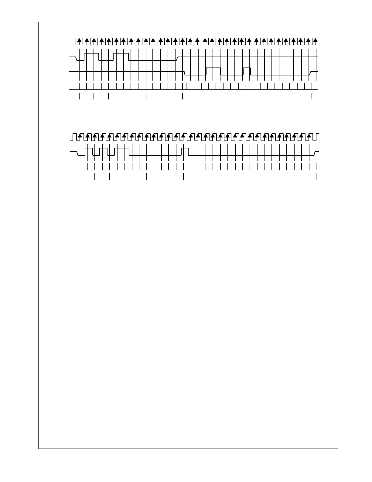
Figure 4. Typical MDC/MDIO Read Operation
MDC
MDIO
(STA)
Z
00011110000000
Idle Start
Opcode
(Write)
PHY Address
(PHYAD = 0Ch)
Register Address
(00h = BMCR)
Figure 5. Typical MDC/MDIO Write Operation
3.3.3 Serial Management Preamble Suppression
The DP83848J supports a Preamble Suppression mode
as indicated by a one in bit 6 of the Basic Mode Status
Register (BMSR, address 01h.) If the station management
entity (i.e. MAC or other management controller) determines that all PHYs in the system support Preamble Suppression by returning a one in this bit, then the station
management entity need not generate preamble for each
management transaction.
The DP83848J requires a single initialization sequence of
32 bits of preamble following hardware/software reset.
This requirement is generally met by the mandatory pullup resistor on MDIO in conjunction with a continuous
MDC, or the management access made to determine
whether Preamble Suppression is supported.
While the DP83848J requires an initial preamble
sequence of 32 bits for management initialization, it does
not require a full 32-bit sequence between each subsequent transaction. A minimum of one idle bit between
management transactions is required as specified in the
IEEE 802.3u specification.
Z
Z
Z
0 0 011000100000000
TA
0 0 0 000 00000000
1000
TA
Register Data
Register Data
Z
Z
Idle
ZZ
Z
Idle
www.national.com 22
4.0 Architecture
This section describes the operations within each transceiver module, 100BASE-TX and 10BASE-T. Each operation consists of several functional blocks and described in
the following:
— 100BASE-TX Transmitter
— 100BASE-TX Receiver
— 10BASE-T Transceiver Module
4.1 100BASE-TX TRANSMITTER
The 100BASE-TX transmitter consists of several functional
blocks which convert synchronous 4-bit nibble data, as provided by the MII, to a scrambled MLT-3 125 Mb/s serial
data stream. Because the 100BASE-TX TP-PMD is integrated, the differential output pins, PMD Output Pair, can
be directly routed to the magnetics.
DP83848J
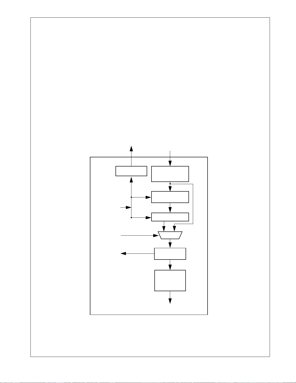
The block diagram in Figure 6. provides an overview of
each functional block within the 100BASE-TX transmit section.
The Transmitter section consists of the following functional
blocks:
— Code-group Encoder and Injection block
— Scrambler block (bypass option)
— NRZ to NRZI encoder block
— Binary to MLT-3 converter / Common Driver
The bypass option for the functional blocks within the
100BASE-TX transmitter provides flexibility for applications
where data conversion is not always required. The
DP83848J implements the 100BASE-TX transmit state
machine diagram as specified in the IEEE 802.3u Standard, Clause 24.
125MHZ CLOCK
BP_SCR
100BASE-TX
LOOPBACK
TX_CLK
DIVIDE
BY 5
MLT[1:0]
TXD[3:0] /
TX_EN
4B5B CODE-GROUP
ENCODER &
INJECTOR
5B PARALLEL
TO SERIAL
SCRAMBLER
MUX
NRZ TO NRZI
ENCODER
BINARY
TO MLT-3 /
COMMON
DRIVER
PMD OUTPUT PAIR
Figure 6. 100BASE-TX Transmit Block Diagram
23 www.national.com

Table 6. 4B5B Code-Group Encoding/Decoding
DATA CODES
DP83848J
IDLE AND CONTROL CODES
INVALID CODES
Note: Control code-groups I, J, K, T and R in data fields will be mapped as invalid codes, together with RX_ER asserted.
0 11110 0000
1 01001 0001
2 10100 0010
3 10101 0011
4 01010 0100
5 01011 0101
6 01110 0110
7 01111 0111
8 10010 1000
9 10011 1001
A 10110 1010
B 10111 1011
C 11010 1100
D 11011 1101
E 11100 1110
F 11101 1111
H 00100 HALT code-group - Error code
I 11111 Inter-Packet IDLE - 0000 (
J 11000 First Start of Packet - 0101 (Note 1)
K 10001 Second Start of Packet - 0101 (Note 1)
T 01101 First End of Packet - 0000 (Note 1)
R 00111 Second End of Packet - 0000 (Note 1)
V 00000
V 00001
V 00010
V 00011
V 00101
V 00110
V 01000
V 01100
Note 1)
www.national.com 24
 Loading...