

Page 1
February 2002
DP83847 DsPHYTER II — Single 10/100 Ethernet Transceiver
DP83847 DsPHYTER II — Single 10/100 Ethernet Transceiver
General Description
The DP83847 is a full feature single Physical Layer device
with integrated PMD sublayers to support both 10BASE-T
and 100BASE-TX Ethernet protocols over Category 3 (10
Mb/s) or Category 5 unshielded twisted pair cables.
The DP83847 is designed for easy implementation of
10/100 Mb/s Ethernet hom e or office solutions. It in terfa ce s
to Twisted Pair media via an external transformer. This
device interface s direc tly to M A C de vi ces th roug h the IEEE
802.3u standard Media Independent Interface (MII) ensuring interoperability between products from different vendors.
The DP83847 utilizes on chip Digital Signal Processing
(DSP) technology and digital Phase Lock Loops (PLLs) for
robust performance under all operating conditions,
enhanced noise immunity, and lower external component
count when compared to analog solutions.
Applications
■ LAN on Motherboard
■ Embedded Applications
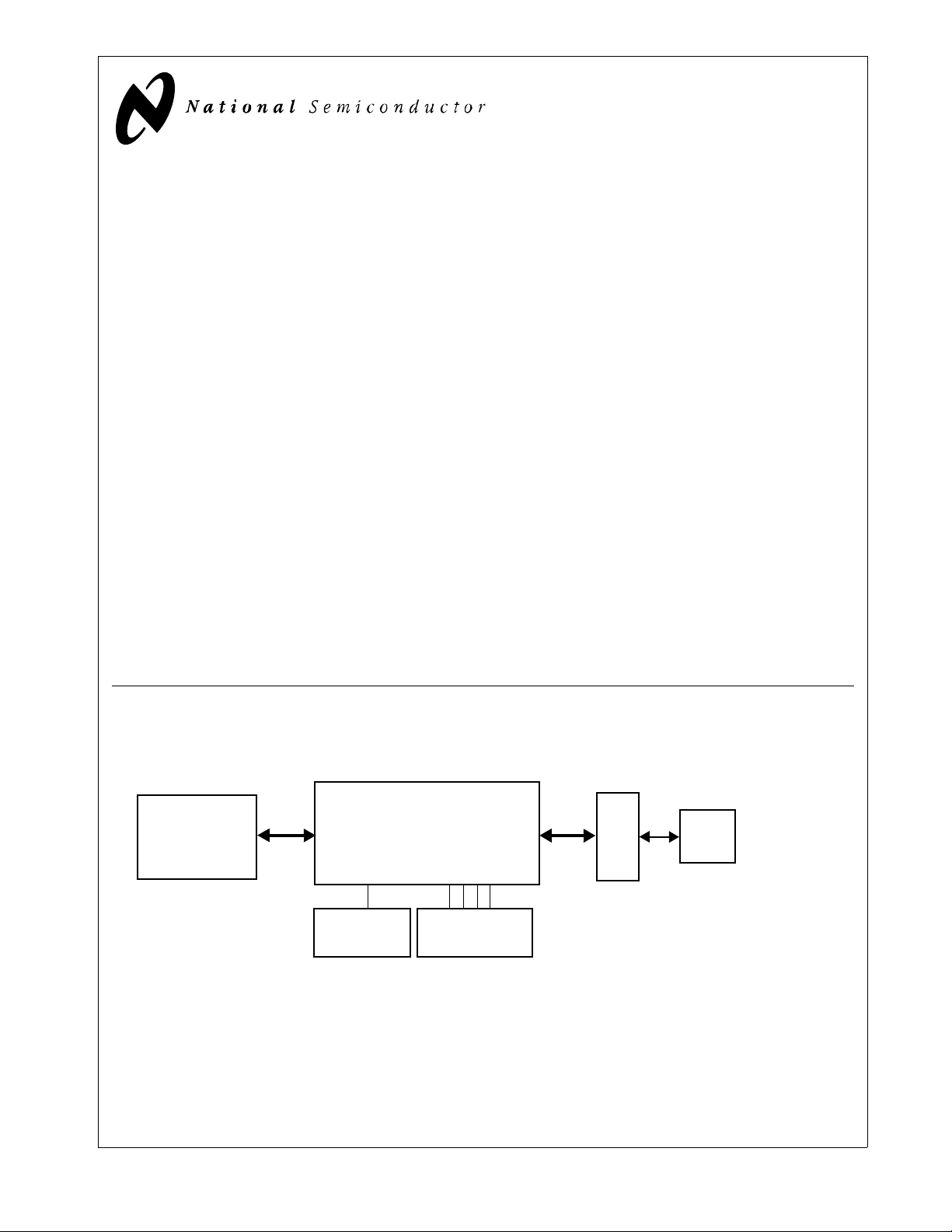
System Diagram
Features
■ Low-power 3.3V, 0.18µm CMOS technology
■ Power consumption < 351mW (typical)
■ 5V tolerant I/Os
■ 5V/3.3V MAC interface
■ IEEE 802.3 ENDEC, 10BASE-T transceivers and filters
■ IEEE 802.3u PCS, 100BASE-TX transceivers and filters
■ IEEE 802.3 compliant Auto-Negotiation
■ Output edge rate control eliminates external filtering for
Transmit outputs
■ BaseLine Wander compensation
■ IEEE 802.3u MII (16 pins/port)
■ LED support (Link, Rx, Tx, Duplex, Speed, Collision)
■ Single register access for complete PHY status
■ 10/100 Mb/s packet loopback BIST (Built in Self Test)
■ 56-pin LLP package (9w) x (9l) x (.75h) mm
Ethernet MAC
MII
25 MHz
Clock
©2002 National Semiconductor Corporation
DP83847
10/100 Mb/s
DsPHYTER II
Status
LEDs
Typical DsPHYTER II application
Magnetics
RJ-45
10BASE-T
or
100BASE-TX
www.national.com
Page 2
MII
DP83847
HARDWARE
CONFIGURATION
PINS
(AN_EN, AN0, AN1)
(PAUSE_EN)
(LED_CFG, PH YAD)
TX_DATA
TRANSMIT CHANNELS &
STATE MACHINES
100 Mb/s 10 Mb/s
4B/5B
ENCODER
PARALLEL TO
SERIAL
SCRAMBLER
NRZ TO NRZI
ENCODER
BINARY TO
MLT-3
ENCODER
10/100 COMMON
OUTPUT DRIVER
TX_CLK
TXD[3:0]
TX_DATA
NRZ TO
MANCHESTER
ENCODER
LINK PULSE
GENERATOR
TRANSMIT
FILTER
TX_ER
TX_CLK
SERIAL
MANAGEMENT
TX_EN
MDIO
MII INTERFACE/ CO NTROL
REGISTERS
PHY ADDRESS
AUTO
NEGOTIATION
BASIC MODE
CONTROL
PCS CONTROL
10BASE-T
100BASE-TX
AUTO-NEGOTIATION
STATE MACHINE
CLOCK
GENERATION
MII
COL
MDC
CRS
RX_DV
RX_ER
RX_DATARX_CLK
RECEIVE CHANNELS &
4B/5B
DECODER
CODE GROUP
ALIGNMENT
SERIAL TO
PARALLEL
DESCRAMBLER
NRZI TO NRZ
DECODER
CLOCK
RECOVERY
MLT-3 TO
BINARY
DECODER
ADAPTIVE
BLW
AND EQ
COMP
RXD[3:0]
STATE MACHINES
100 Mb/s 10 Mb/s
RX_CLK
RX_DATA
RX_CLK
MANCHESTER
TO NRZ
DECODER
CLOCK
RECOVERY
LINK PULSE
DETECTOR
RECEIVE
FILTER
SMART
SQUELCH
TD±
LED
DRIVERS
LEDS
SYSTEM CLOCK
REFERENCE
Figure 1. Block Diagram of the 10/100 DSP based core.
2 www.national.com
10/100 COMMON
INPUT BUFFER
RD±
Page 3

Table of Content
1.0 Pin Descriptions . . . . . . . . . . . . . . . . . . . . . . . . . . . . . . .5
1.1 MII Interfa ce . . . . . . . . . . . . . . . . . . . . . . . . . . . . . . 5
1.2 10 Mb/s and 100 Mb/s PMD Interface . . . . . . . . . .6
1.3 Clock Inte r fa ce . . . . . . . . . . . . . . . . . . . . . . . . . . . . 7
1.4 Special Connections . . . . . . . . . . . . . . . . . . . . . . . 7
1.5 LED Interfa ce . . . . . . . . . . . . . . . . . . . . . . . . . . . . . 7
1.6 Strapping Options/Dua l Pu r p o se Pins . . . . . . . . . . 8
1.7 Reset . . . . . . . . . . . . . . . . . . . . . . . . . . . . . . . . . . . 9
1.8 Power and Ground Pin . . . . . . . . . . . . . . . . . . . . . 9
1.9 Package Pin Assignments . . . . . . . . . . . . . . . . . .10
2.0 Confi guration . . . . . . . . . . . . . . . . . . . . . . . . . . . . . . . . 11
2.1 Auto-Negotiation . . . . . . . . . . . . . . . . . . . . . . . . .11
2.2 PHY Address and LEDs . . . . . . . . . . . . . . . . . . . 12
2.3 LED INTERFACES . . . . . . . . . . . . . . . . . . . . . . .13
2.4 Half Duple x vs. Full Dup l e x . . . . . . . . . . . . . . . . . 13
2.5 MII Isolate Mode . . . . . . . . . . . . . . . . . . . . . . . . .14
2.6 Loopback . . . . . . . . . . . . . . . . . . . . . . . . . . . . . . .14
2.7 BIST . . . . . . . . . . . . . . . . . . . . . . . . . . . . . . . . . . . 14
3.0 Functional Description . . . . . . . . . . . . . . . . . . . . . . . . .15
3.1 802.3u MII . . . . . . . . . . . . . . . . . . . . . . . . . . . . . .15
3.2 100BASE-TX TRANSMITTER . . . . . . . . . . . . . . .16
3.3 100BASE-TX RECEIVER . . . . . . . . . . . . . . . . . . 20
3.4 10BASE-T TRANSCEIVER M OD ULE . . . . . . . . . 23
3.5 TPI Networ k Ci rcuit . . . . . . . . . . . . . . . . . . . . . . . 24
3.6 ESD Protect i o n . . . . . . . . . . . . . . . . . . . . . . . . . .25
3.7 Crystal Osci llato r Circuit . . . . . . . . . . . . . . . . . . .26
3.8 Reference Bypass Couple . . . . . . . . . . . . . . . . . .26
4.0 Reset Operation . . . . . . . . . . . . . . . . . . . . . . . . . . . . . . 26
4.1 Hardware R e se t . . . . . . . . . . . . . . . . . . . . . . . . . . 26
4.2 Software R e s e t . . . . . . . . . . . . . . . . . . . . . . . . . .26
5.0 Regis t e r B lo c k . . . . . . . . . . . . . . . . . . . . . . . . . . . . . . . 27
5.1 Register Definition . . . . . . . . . . . . . . . . . . . . . . . .29
5.2 Extended Registers . . . . . . . . . . . . . . . . . . . . . . .37
6.0 Elect rical Speci fications . . . . . . . . . . . . . . . . . . . . . . .44
6.1 Reset Timi n g . . . . . . . . . . . . . . . . . . . . . . . . . . . . 46
6.2 PGM Clock Timing . . . . . . . . . . . . . . . . . . . . . . .47
6.3 MII Serial Management Timing . . . . . . . . . . . . . .47
6.4 100 Mb/s Timing . . . . . . . . . . . . . . . . . . . . . . . . .48
6.5 10 Mb/s Tim i n g . . . . . . . . . . . . . . . . . . . . . . . . . .52
6.6 Loopback Timing . . . . . . . . . . . . . . . . . . . . . . . . .57
6.7 Isolation Timing . . . . . . . . . . . . . . . . . . . . . . . . . .59
7.0 Physical Dimensions . . . . . . . . . . . . . . . . . . . . . . . .60
DP83847
3 www.national.com
Page 4
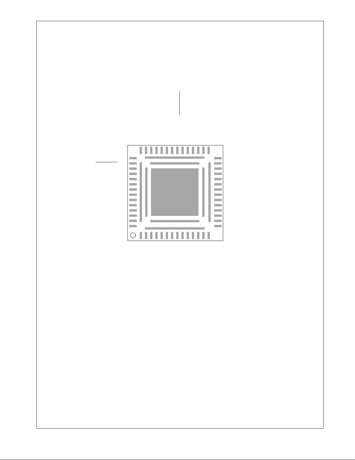
Pin Layout
42 C1
41 TXD_3
40 TXD_2
39 TXD_1
38 TXD_0
37 TX_EN
36 TX_CLK
35 TX_ER
DP83847
34 RESERVED
33 RX_ER/PAUSE_EN
32 RX_CLK
31 RX_DV
30 RXD_0
29 RXD_1
COL 43
RESERVED 44
CRS/LED_CFG
RESET 46
RESERVED 47
X2 48
X1 49
RESERVED 50
RESERVED 51
RESERVED 52
RESERVED 53
RESERVED 54
RESERVED 55
VDD 56
45
61
59
RESERVED 1
62
60
65 Gnd
64
63
58
57
RD+ 7
RD - 6
RBIAS 3
RESERVED 2
RESERVED 4
RESERVED 5
TD- 11
TD+ 10
RESERVED 8
RESERVED 9
RESERVED 12
VDD 14
RESERVED 13
28 VDD
27 RXD_2
26 RXD_3
25 MDC
24 MDIO
23 LED_DPLX/PHYAD0
22 LED_COL/PHYAD1
21 LED_GDLNK/PHYAD2
20 LED_TX/PHYAD 3
19 LED_RX/PHYAD4
18 LED_SPEED
17 AN_EN
16 AN_1
15 AN_0
Top View
Leadless Leadframe Package (LLP)
Order Number DP83847 ALQA 5 6A
NS Package Number LQA-56A
Note 1: Pins 57 to 65 required soldering care. Check Package Instruction, AN-1187, for details.
4 www.national.com
Page 5

1.0 Pin Descriptions
The DP83847 pins are c lassifi ed into the fol lowing i nterfac e
categories (each interface is described in the sections that
follow):
— MII Interface
— 10/100 Mb/s PMD Interface
— Clock Interface
— Special Connect Pins
— LED Interface
— Strapping Options/Dual Function pins
—Reset
— Power and Ground pins
Note: Strapping pin option (BOLD) Please see Section 1.6
for strap definitions.
1.1 MII Interface
Signal Name Type LLP Pin # Description
MDC I 25 MANAGEMENT DATA CLOCK: Synchronous clock to the M DIO
MDIO I/O, OD 24 MANAGEMENT DATA I/O: Bi-directional management instruc-
CRS/LED_CFG
COL O 43 COLLISION DETECT: Asserted high to indicate detection of a
O, S 45 CARRIER SENSE: Asserted high to indicate the presence of car-
All DP83847 signal pins are I/O cells regardless of the particular use. Below definitions define the functionality of the
I/O cells for each pin.
Type: I Inputs
Type: O Outputs
Type: I/O Input/Output
Type OD Open Drain
Type: PD,PU Internal Pulldown/Pullup
Type: S Strapping Pin (All strap pins except PHY-
AD[0:4] have internal pull-ups or pulldowns. If the default strap value is needed
to be changed then an ext ernal 5 kΩ resistor
should be used. Please see Table 1.6 on
page 8 for details.)
management data input/output serial interface which may be
asynchronous to transmit and receive clocks. The maximum clock
rate is 25 MHz with no minimum clock rate.
tion/data signal th at m ay be s ourc ed by th e st ation management
entity or the PHY. This pin requires a 1.5 kΩ pullup resistor.
rier due to receive or transmit activity in 10BASE-T or 100BASETX Half Duple x Mo des , while in full du ple x mo de ca rrier sense is
asserted to indicate the presence of car rier due only to re ceive activity.
collision condition (simultaneous transmit and receive activity) in
10 Mb/s and 100 Mb/s Half Duplex Modes.
While in 10BASE-T Half Duplex mode with Heart beat enabled this
pin are also asserted for a duration of approximately 1µs at the
DP83847
5 www.national.com
Page 6

Signal Name Type LLP Pin # Description
RXD[3]
RXD[2]
RXD[1]
RXD[0]
RX_ER/PAUSE_EN
RX_DV O 31 RECEIVE DATA VALID: Asserted high to indi ca te that va lid data
O, PU/PD 26, 27, 29, 30RECEIVE DATA: Nibble wide receive data (synchronous to cor-
responding RX_CLK, 25 MHz for 100BASE-TX mode, 2.5 MHz
for 10BASE-T nibble mode). Data is driven on the falling edge of
RX_CLK. RXD[2] has an internal pull-down resistor. The remaining RXD pins have pull-ups.
S, O, PU 33 RECEIVE ERROR: Asserted high to indi ca te t hat an invalid s ym-
bol has been detected within a received packet in 100BASE-TX
mode.
is present on the corresponding RXD[3:0] for nibble mode. Data
is driven on the falling edge of the corresponding RX_CLK.
1.2 10 Mb/s and 100 Mb/s PMD Interface
Signal Name Type LLP Pin # Description
TD+, TD- O 10, 11 Differential comm on dri ver tran smit output . Th ese di fferenti al out -
RD-, RD+ I 6, 7 Differential receive input. These differential inputs can be config-
puts are configurable to e ither 10BASE-T o r 100BASE- TX sig naling.
The DP83847 will a utomat ically con figure th e common dri ver out puts for the proper signal type as a result of either forced configuration or Auto-Negotiation.
ured to accept either 100BASE-TX or 10BASE-T signaling.
The DP83847 will automatically configure the receive inputs to
accept the proper signal type as a result of either forced configuration or Auto-Negotiation.
DP83847
6 www.national.com
Page 7

1.3 Clock Interface
Signal Name Type LLP Pin # Description
X1 I 49 REFERENCE CLOCK INPUT 25 MHz: This pin is the primary
clock reference inpu t for the DP 8384 7 and mu st be c onnect ed to
a 25 MHz 0.005% (±50 ppm) clock source. The DP83847 supports CMOS-level oscillator sources.
X2 O 48 REFERENCE CLOCK OUTPUT 25 MHz: This pin is the primary
clock reference output.
1.4 Special Connections
Signal Name Type LLP Pin # Description
RBIAS I 3 Bias Resistor Connection. A 10.0 kΩ 1% resist or shou ld be con-
nected from RBIAS to GND.
C1 O 42 Reference Bypass Re gulator. Parall el caps, 10µ F (Tantalum pre-
RESERVED I/O 1, 2, 4, 5, 8,
9, 12, 13,
34, 44, 47,
50, 51, 52,
53, 54, 55,
61
ferred) and .1µF, should be placed close to C1 and connected to
GND. See Section 3.8 for proper placement.
RESERVED: These pins must be left unconnected
DP83847
1.5 LED Interface
Signal Name Type LLP Pin # Description
LED_DPLX/PHYAD0 S, O 23 FULL DUPLEX LED STATUS: Indicates Full-Duplex status.
LED_COL/PHYAD1 S, O 22 COLLISION LED STATUS: Indicates Collision activity in Half Du-
LED_GDLNK/PHYAD2 S, O 21 GOOD LINK LED STATUS: Indicates Good Link Status for
LED_TX/PHYAD3 S, O 20 TRANSMIT LED STATUS: Indicates transmit activity. LED is on
LED_RX/PHYAD4 S, O 19 RECEIVE LED STATUS: Indicates receive act iv ity. LED is on fo r
LED_SPEED O 18 SPEED LED STATUS: Indicates link speed; high for 100 Mb/s,
plex mode.
10BASE-T and 100BASE-TX.
for activity, off for no activity.
activity, off for no activity.
low for 10 Mb/s.
7 www.national.com
Page 8
1.6 Strapping Options/Dual Purpose Pins
A 5 kΩ resistor should be used for pull-down or pull-up to
change the default strap option. If the default option is
required, then there is no need for external pull-up or pull
down resistors, sinc e the int ernal pu ll-up or p ull down re sis-
Signal Name Type LLP Pin # Description
LED_DPLX/PHYAD0
LED_COL/PHYAD1
LED_GDLNK/PHYAD2
LED_TX/PHYAD3
LED_RX/PHYAD4
AN_EN
AN_1
AN_0
S, O 23
22
21
20
19
S, O, PU 17
16
15
PHY ADDRESS [4:0]: The DP83847 provid es fiv e PHY address
pins, the state of which a re latc hed in to the PHYC TRL regi ster at
system Hardware-Reset.
The DP83847 supports PHY Address strapping values 0
(<00000>) through 31 (<1 1111>). PHY Address 0 puts the part
into the MII Isolate Mode. The MII isolate mode must be selecte d
by strapping Phy Address 0; changing to Address 0 by register
write will not put the Phy in the MII isolate mode.
The status of these pins are latc hed into the PHY Control Regi ster
during Hardware-Reset. (Pleas e note the se pins have no internal
pull-up or pull-down resistors and they must be strapped high or
low using 5 kΩ resistors.)
Auto-Negotiation Enable: When high enab les Auto-N egotiation
with the capability set by AN O and AN1 pins. W hen low , puts the
part into Forced Mode with the capability set by AN0 and AN1
pins.
AN0 / AN1: These input pins control the forced or advertised operating mode of the DP83847 according to the following table.
The value on these pins is set by connecting the input pins to
GND (0) or V
NEVER be connected directly to GND or V
The value set at this input is latched into the DP83847 at Hardware-Reset.
The float/pull-down sta tus of these pin s ar e latch ed into the Bas ic
Mode Control Register and the Auto_Negotiation Advertisement
Register during Hardware-Reset. After res et is deasserte d, these
pins may switch to outputs so if pull-ups or pull-downs are i m plemented, they should be pulled through a 5 kΩ resistor.
The default is 111 since these pins have pull-ups.
tors will set the default value. Please note that the
PHYAD[0:4] pins have no internal pull-ups or pull-downs
and they must be strapped. Since these pins may have
alternate functions after reset is deasserted, they should
not be connected directly to Vcc or GND.
(1) through 5 kΩ resistors. These pins should
CC
CC.
DP83847
AN_EN AN1 AN0 Forced Mode
0 0 0 10BASE-T, Half-Duplex
0 0 1 10BASE-T, Full-Duplex
0 1 0 100BASE-TX, Half-Duplex
0 1 1 100BASE-TX, Full-Duplex
AN_EN AN1 AN0 Advertised Mode
1 0 0 10BASE-T, Half/Full-Duplex
1 0 1 100BASE-TX, Half /Full-Duplex
1 1 0 10BASE-T Half-Duplex
100BASE-TX, Half-Duplex
1 1 1 10BASE-T, Half/Full-Duplex
100BASE-TX, Half/Full-Duplex
8 www.national.com
Page 9

Signal Name Type LLP Pin # Description
RX_ER/PAUSE_EN S, O, PU 33 PAUSE ENABLE: This strapping option allows advertisement of
whether or not the DTE(MAC) h as imp lemented b oth the op tional
MAC control sublayer and the pause function as specified in
clause 31 and annex 31B of the IEEE 802.3x specification (Full
Duplex Flow Control).
When left floating the Auto-Negotiation Advertisement Register
will be set to 0, i ndicatin g that Ful l Duplex Fl ow Contro l is not sup ported.
When tied low through a 5 kΩ, the Auto-Negotiation Advertise-
ment Registe r will be set to 1 , indicating th at Full Duplex Fl ow
Control is supported.
The float/ pul l-do wn st atu s of th is pi n is latc hed int o th e Aut o- Negotiation Advertisement Register during Hardware-Reset.
CRS/LED_CFG
S, O
PU
,
45 LED CONFIGURATION: This strapping option defines th e polar-
ity and function of the FDPLX LED pin.
See Section 2.3 for further descriptions of this strapping option.
1.7 Reset
Signal Name Type LLP Pin # Description
RESET
I46RESET: Active Low input that initializes or re-initializes the
DP83847. Asserting thi s pin low fo r at least 1 60 µs wil l force a reset process to occu r which wi ll result in all intern al registe rs re-initializing to their default states as specified for each bit in the
Register Block sect ion and all s trappin g options are re-initialized .
DP83847
1.8 Power and Ground Pin
Signal Name LLP Pin # Description
TTL/CMOS INPUT/OUTPUT SUPPLY
IO_VDD 28, 56 I/O Supply
IO_GND GND I/O Ground
INTERNAL SUPPLY PAIRS
CORE_VDD Internal Digital Core Supply
CORE_GND GND Digital Core Ground
ANALOG SUPPLY PINS
ANA_VDD 14 Analog Supply
ANA_GND GND Analog Ground
SUBSTRATE GROUND
SUB_GND GND Bandgap Substrate connection
9 www.national.com
Page 10
1.9 Package Pin Assignments
LLP Pin # Pin Name
1 RESERVED
2 RESERVED
3 RBIAS
4 RESERVED
5 RESERVED
6 RD7 RD+
8 RESERVED
9 RESERVED
10 TD+
11 TD12 RESERVED
13 RESERVED
14 VDD (ANA_VDD)
15 AN_0
16 AN_1
17 AN_EN
18 LED_SPEED
19 LED_RX /PHYAD4
20 LED_TX /PHYAD3
21 LED_GDLNK/PHYAD2
22 LED_COL /PHYAD1
23 LED_FDPLX /PHYAD0
24 MDIO
25 MDC
26 RXD_3
27 RXD_2
28 VDD (IO_VDD)
29 RXD_1
30 RXD_0
31 RX_DV
32 RX_CLK
33 RX_ER/
34 RESERVED
35 TX_ER
36 TX_CLK
37 TX_EN
38 TXD_0
39 TXD_1
40 TXD_2
41 TXD_3
42 C1
PAUSE_EN
LLP Pin # Pin Name
43 COL
44 RESERVED
45 CRS/
46 RESET
47 RESERVED
48 X2
49 X1
50 RESERVED
51 RESERVED
52 RESERVED
53 RESERVED
54 RESERVED
55 RESERVED
56 VDD (IO_VDD)
57 VDD
58 GND
59 VDD
60 GND
61 RESERVED
62 GND
63 VDD
64 GND
65 GND
LED_CFG
DP83847
10 www.national.com
Page 11

2.0 Configuration
This section in clude s inform atio n on the var ious con figura tion options available with the DP83847. The configuration
options described below include:
— Auto-Negotiation
— PHY Address and LEDs
— Half Duplex vs. Full Dup lex
— Isolate mode
— Loopback mode
—BIST
2.1 Auto-Negotiation
The Auto-Negotiation function provides a mechanism for
exchanging configuration information between two ends of
a link segment and automatically selecting the highest performance mode of operation supported by both devices.
Fast Link Pulse (FLP) Bursts provide the signalling used to
communicate Auto-Negotiation abilities between two
devices at each end of a link segment. For further detail
regarding Auto-Negotiation, refer to Clause 28 of the IEEE
802.3u specification. The DP83847 supports four different
Ethernet protocols (10 Mb/s Half Duplex, 10 Mb/s Full
Duplex, 100 Mb/s Half Duplex, and 100 Mb/s Full Duplex),
so the inclusion of Auto-Negotiation ensures that the highest performance protocol will be selected based on the
advertised ability of the Link Partner. The Auto-Negotiation
function within the DP83847 can be controlled either by
internal register access or by the use of the AN_EN, AN1
and AN0 pins.
2.1.1 Auto-Negotiation Pin Control
The state of AN_EN, AN0 an d AN1 det ermine s wheth er the
DP83847 is forced in to a specific mode or Aut o-Negoti ation
will advertise a s pe cif ic ab ili ty (o r s et of abi lities) as given i n
Table 1. These pins allow configuration options to be
selected without requiring internal register access.
The state of AN _EN, AN0 and A N1, upon po wer-up/ reset,
determines the state of bits [8:5] of the ANAR register.
The Auto-Negotiation function selected at power-up or
reset can be cha nged at any time by writin g to the Basic
Mode Contro l Register (B MCR) at address 00h.
DP83847
Table 1. Auto-Negotiation Modes
AN_EN AN1 AN0 Forced Mode
0 0 0 10BASE-T, Half-Duplex
0 0 1 10BASE-T, Full-Duplex
0 1 0 100 BASE-TX, Half-Du ple x
0 1 1 100 BASE-TX, Ful l-Dup lex
AN_EN AN1 AN0 Advertised Mode
1 0 0 10BASE-T, Half/Full-Duplex
1 0 1 100 BASE-TX, Half/ Ful l-Dup lex
1 1 0 10BASE-T Half-Duplex
100BASE-TX, Half-Duplex
1 1 1 10BASE-T, Half/Full-Duplex
100BASE-TX, Half/Full-Duplex
2.1.2 Auto-Negotiation Register Control
When Auto-Negotiation is enabled, the DP83847 transmits
the abilit ies program med into the Au to-Negotia tion Advertisement register (ANAR) at address 04h via FLP Bursts.
Any combination of 10 Mb/s, 100 Mb/s, Half-Duplex, and
Full Duplex modes may be selected.
The BMCR provides software with a mechanism to control
the operation of the DP83847. The AN0 and AN1 pins do
not affect the c ont ents of the BMCR a nd ca nno t be used by
software to obtain status of the mode selected. Bits 1 & 2 of
the PHYSTS register are only valid if Auto-Negotiation is
disabled or after Auto-Negotiation is complete. The AutoNegotiation protocol compares the contents of the
ANLPAR and ANAR registers and uses the results to automatically configure to the highest performance protocol
between the local and far-end port. The results of AutoNegotiation (Auto-Neg Complete, Duplex Status and
Speed) may be accessed in the PHYSTS register.
Auto-Negotiation Priority Resolution:
— (1) 100BASE-TX Full Duplex (Highest Priority)
— (2) 100BASE-TX Half Duplex
— (3) 10BASE-T Full Duplex
— (4) 10BASE-T Half Duplex (Lowest Priority)
The Basic Mode Control Register (BMCR) at address 00h
provides control for enabling, disabling, and restarting the
Auto-Negotiation process. When Auto-Negotiation is disabled the Speed Selectio n bi t in the BMCR controls switching between 10 Mb/s or 100 Mb/s operation, and the
Duplex Mode bit controls switching between full duplex
operation and half duplex operation. The Speed Selection
and Duplex Mode bits have no effect on the mode of operation when the Auto-Negotiation Enable bit is set.
The Basic Mode Status Register (BMSR) indicates the set
of available abilities for technology types, Auto-Negotiation
ability, and Extended Register Capability. These bits are
permanently set to indicate the full functionality of the
DP83847 (only the 100BASE-T4 bit is not set since the
DP83847 does not support that function).
11 www.national.com
Page 12

The BMSR also provides status on:
— Whether Auto-Negotiation is complete
— Whether the Link Partner is advertising that a remote
fault has occurred
— Whether valid link has been established
— Support for Management Frame Preamble suppression
The Auto-Negotiation Advertisement Register (ANAR) indi-
cates the Auto-Negotiation abilities to be advertised by the
DP83847. All available abilities are transmitted by default,
but any ability can be suppressed by writing to the ANAR.
Updating the ANAR to suppress an ability is one way for a
management agent to ch ange (forc e) the tech nolog y that is
used.
The Auto-Negotiation Link Partner Ability Register
(ANLPAR) at address 05h is used to receive the base link
code word as wel l as all next page code word s during the
negotiati on. Furthermore, the ANLPAR will be updat ed to
either 0081h or 0021h for parallel detection to either 100
Mb/s or 10 Mb/s respectively.
The Auto-Negotiation Expansion Register (ANER) indicates additional Auto-Negotiation status. The ANER provides status on:
— Whether a Parallel Detect Fault has occurred
— Whether the Link Partner supports the Next Page func-
tion
— Whether the DP83847 supports the Next Page function
— Whether the current page being exchanged by Auto -Ne-
gotiation has been received
— Whether the Link Partner supports Auto-Negotiation
2.1.3 Auto-Negotiation Parallel Detection
The DP83847 supports the Parallel Detection function as
defined in the IEEE 802.3u specifi ca tio n. Para lle l De tect io n
requires both the 10 Mb/s and 100 Mb/s receivers to monitor the receive signal and report link status to the AutoNegotiation function. Auto-Negotiation uses this information to configure th e correct t echno logy i n the e vent th at the
Link Partner does not support Auto-Negotiation but is
transmitting link signals that the 100BASE-TX or 10BASET PMAs recognize as valid link signa ls .
If the DP83847 completes Auto-Negotiation as a result of
Parallel Detection, bits 5 and 7 within the ANLPAR register
will be set to reflect the mode of operation present in the
Link Partner. Note that bits 4:0 of the ANLPAR will also be
set to 00001 based on a successful parallel detection to
indicate a valid 802.3 selector field. Software may determine that negotiation completed via Parallel Detection by
reading a zero in the Link Partner Auto-Negotiation Able
bit, once the Auto-Negotiation Com ple te bit is set. If configured for parallel detect mode and any condition other than
a single good link occurs then the parallel detect fault bit
will set.
2.1.4 Auto-Negotia tion Rest art
Once Auto-Negotiation has completed, it may be restarted
at any time by setting bit 9 (Res tart Auto- Negotiat ion) of th e
BMCR to one. If the mode confi gured b y a su cces sful Au toNegotiation loses a valid link, then the Auto-Negotiation
process will resume and attempt to determine the configuration for the link. This function ensures that a valid configuration is maintained if the cable becomes disconnected.
DP83847
A renegotiation requ es t fro m a ny en tity, such as a management agent, will cause the DP83847 to halt any transmit
data and link pulse activity until the break_link_timer
expires (~1500 ms). Consequently, the Link Partner will go
into link fail and normal Auto-Negotiation resumes. The
DP83847 will resume Auto-Negotiation after the
break_link_timer has expired by issuing FLP (Fast Link
Pulse) bursts.
2.1.5 Enabling Auto-Negotiation via Software
It is important to note that if the DP83847 has been initialized upon power-up as a non-auto-negotiating device
(forced technology), and it is then requ ire d that Auto-Negotiation or re-Auto-Negotiation be initiated via software,
bit 12 (Auto-Negotiation Enable) of the Basic Mode Control
Register must first be cleared and then set for any AutoNegotiation function to take effect.
2.1.6 Auto-Negotiation Complete Time
Parallel detection and Auto-Negotiation take approximately
2-3 seconds to co mp let e. In addition, Auto-Neg otia tion with
next page should take approximately 2-3 seconds to complete, depending on the number of next pages sent.
Refer to Clause 28 of the IEEE 802.3u standard for a full
description of the individual timers related to Auto-Negotiation.
2.2 PHY Address and LEDs
The 5 PHY address inputs pins are shared with the LED
pins as shown below.
Table 2. PHY Address Mapping
Pin # PHYAD Function LED Function
23 PHYAD0 Duplex
22 PHYAD1 COL
21 PHYAD2 Good Link
20 PHYAD3 TX Activity
19 PHYAD4 RX Activity
18 n/a Speed
The DP83847 can be set to respond to any of 32 possible
PHY addresses. Each DP83847 or port sharing an MDIO
bus in a system must have a unique physical address.
Refer to Section 3.1.4, PHY Address Sensing section for
more details.
The state of each of the PHYAD inputs latched into the
PHYCTRL register bits [4:0]at system power-up/reset
depends on whether a pull-up or pull-down resistor has
been installed for each pin. For further detail relating to the
latch-in timing requirements of the PHY Address pins, as
well as the other hardware configuration pins, refer to the
Reset summary i n Section 4.0.
Since the PH YAD strap option s sh a re t he LED o utp ut pi n s,
the external components required for strapping and LED
usage must be considered in order to avoid contention.
Specifically, when the LED outputs are used to drive LEDs
directly, the active state of each output driver is dependent
on the logic level sampled by the corresponding PHYAD
input upon power-up/reset. For example, if a given PHYAD
input is resistively pu lle d lo w the n th e co rres pon di ng output
will be configured as an active high driver. Conversely, if a
12 www.national.com
Page 13
given PHYAD input is resistively pulled high, then the corresponding output will be configured as an active low
driver. Refer to Figure 1 for an example of a PHYAD con-
DP83847
nection to external components. In this example, the
PHYAD strapping results in address 00011 (03h).
The adaptive nature of the LED outputs helps to simplify
potential impleme ntation issues of thes e dual purpose pins.
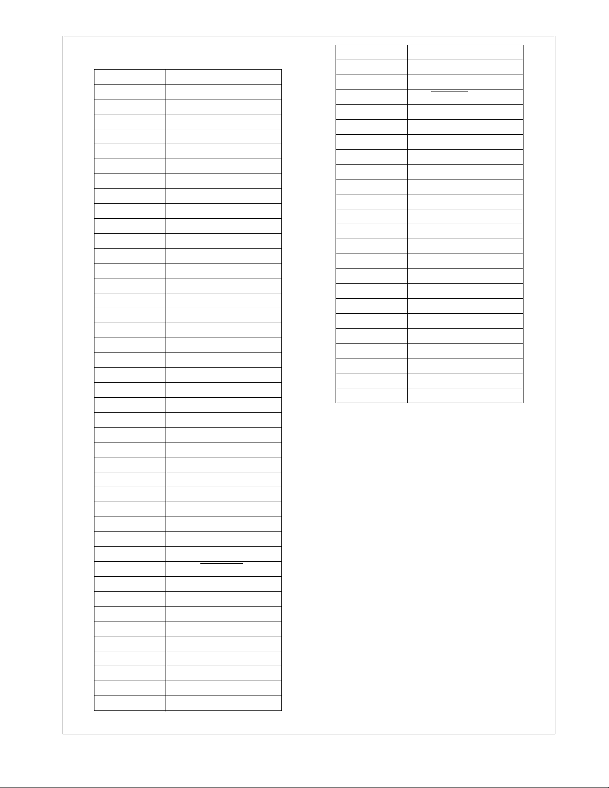
LED_RX
PHYAD4= 0
1kΩ
10kΩ
Figure 1. PHYAD Strapping and LED Loading Example
LED_TX
1kΩ
10kΩ
LED_GDLNK
10kΩ
2.3 LED INTERFACES
The DP83847 has 6 Light Emitting Diode (LED) outputs,
each capable to drive a maximum of 10 mA, to indicate the
status of Link, Transmit, Receive, Collision, Speed, and
Full/Half Duplex operation. The LED_CFG strap option is
used to configure the LED_FDPLX output for use as an
LED driver or more general purpose control pin. See the
table below:
Table 3. LED Mode Select
LED_CFG Mode Description
1 LED polarity adjusted
0 Duplex active-high
The LED_FDPLX pin indicates the Half or Full Duplex configuration of the port in both 10 Mb/s and 100 Mb/s operation. Since t his pin is als o used as th e PHY address strap
option, the polarity of this indicator may be adjusted so that
in the “active” (FULL DUPLEX selected) state it drives
against the pullup/pulldown strap. In this configuration it is
suitable for use as an LED. When LED_CFG is high this
mode is selected and DsPHYTER automatically adjusts the
polarity of the output. If LED_CFG is low, the output drives
high to indicate the “active” state. In this configuration the
output is suitable for use as a control pin. The
LED_SPEED pin indicates 10 or 100 Mb/s data rate of the
port. The stan da rd C M OS dr i ve r go es hi g h wh en op e rat i ng
in 100 Mb/s operation. Since this pin is not utilized as a
strap option, it is not affected by polarity adjustment.
The LED_GDLNK pin indicates the link status of the port.
Since this pin is also used as the PHY address strap
option, the polarity of this indicator is adjusted to be the
inverse of the strap value.
LED_COL
PHYAD2 = 0PHY AD3 = 0
1kΩ
In 100BASE-T mode, link is established as a result of input
receive amplitude compliant with TP-PMD specifications
which will result in internal generation of signal detect.
10 Mb/s Link is estab lishe d as a resu lt of the rec eption of at
least seven consecutive normal Link Pulses or the reception of a valid 10BASE-T packet. This will cause the assertion of GD_LINK. GD_LINK will deassert in accordance
with the Link Loss Timer as specified in IEEE 802.3.
The Collision LED indicates the presence of collision activity for 10 Mb/s or 100 Mb/s Half Duplex operation. This bit
has no meaning in Full Duplex operation and will be deasserted when the port is operating in Full Duplex. Since this
pin is also used as the PHY address strap option, the
polarity of this indicator is adjusted to be the inverse of the
strap value. In 10 Mb/s half duplex mode, the collision LED
is based on the COL signal. When in this mode, the user
should disable the Heartbeat (SQE) to avoid asserting the
COL LED during transmission. See Section 3.4.2 for more
information about the Heartbeat signal.
The LED_RX and LED_TX pins indicate the presence of
transmit and/or receive activity. Since these pins are also
used in PHY address strap options, the polarity is adjusted
to be the inverse of the respective strap values.
PHYAD1 = 1
1kΩ
10kΩ
LED_FDPLX
PHYAD0 = 1
1kΩ
10kΩ
VCC
2.4 Half Duplex vs. Full Duplex
The DP83847 supports both half and full duplex operation
at both 10 Mb/s and 100 Mb/s speeds.
Half-duplex is the standard, traditional mode of operation
which relies on the CSMA/CD protocol to handle collisions
and network access. In Half-Dupl ex mode, CRS responds
to both transmit and receive activity in order to maintain
compliance with IEEE 802.3 specificat ion .
Since the DP83847 is designed to support simultaneous
transmit and receive activity it is capable of supporting full-
13 www.national.com
Page 14

duplex switched ap pli ca tio ns with a throughput of up to 200
Mb/s per port when operating in 100BASE-TX mode.
Because the CSMA/CD protocol does not apply to fullduplex operation, the DP83847 disables its own internal
collision sensing and reporting functions and modifies the
behavior of Carrier Sense (CRS) such that it indicates only
receive act ivity. This allo ws a full-duplex c apable MAC to
operate properly.
All modes of operation (100BASE-TX and 10BASE-T) can
run either half-duplex or full-duplex. Additionally, other than
CRS and Collision reporting, all remaining MII signaling
remains the same regardless of the selected duplex mode.
It is important to understand that while Auto-Negotiation
with the use of Fast Link Pulse code words can interpret
and configure to full-duplex operation, parallel detection
can not recognize the difference between full and halfduplex from a fixed 10 Mb/s or 100 Mb/s link partner over
twisted pair. As specified in 802.3u, if a far-end link partner
is transmitting forced full duplex 100BASE-TX for example,
the parallel detection state machine in the receiving station
would be unable to detect the full duplex capability of the
DP83847
14 www.national.com
Page 15
3.0 Functional Description
DP83847
3.1 802.3u MII
The DP83847 incorporates the Media Independent Interface (MII) as specified in Clause 22 of the IEEE 802.3u
standard. This interface may be used to connect PHY
devices to a MAC in 10/100 Mb/s systems. This section
describes both the serial MI I man age me nt inte rfac e as wel l
as the nibble wide MII data interface.
The serial management interface of the MII allows for the
configuration and control of multiple PHY devices, gathering of status, error in formation, and the de terminati on of th e
type and capabilities of the attached PHY(s).
The nibble wide MII data interfa ce c ons is t s of a rec ei ve bu s
and a transmit bus each with control signals to facilitate
data transfer between the PHY and the upper layer (MAC).
3.1.1 Seri al Managemen t Register Access
The serial management MII specification defines a set of
thirty-two 16-bit status and control registers that are accessible through the management interface pins MDC and
MDIO. The DP83847 implements all the required MII registers as well as several optional registers. These registers
are fully described in Secti on4.0. A description of the serial
management access protocol follows.
3.1.2 Serial Management Access Protocol
The serial control interface consists of two pins, Management Data Clock (MDC) and Management Data Input/Output (MDIO). MDC has a maximum clock rate of 25 MHz
and no minimum rate. The MDIO line is bi-directional and
may be shared by up to 32 devices. The MDIO frame for-
mat is shown below in Table 4: Typical MDIO Frame Format.
The MDIO pin requires a pull-up resistor (1.5 kΩ) which,
during IDLE and turnaro und, w ill pu ll MDIO hi gh. In order to
initialize the MDIO int erface , the st atio n manag ement entit y
sends a sequence of 32 contiguous logic ones on MDIO to
provide the DP83847 with a sequence that can be used to
establish synchronization. This preamble may be generated either by driving MDIO high for 32 consecutive MDC
clock cycles, or by simply allowing the MDIO pull-up resistor to pull the MDIO pin high during which time 32 MDC
clock cycles are provided. In addition 32 MDC clock cycles
should be used to re-sync the device if an invalid start,
opcode, or turnaround bit is detected.
The DP83847 waits until it has received this preamble
sequence before responding to any other transaction.
Once the DP83847 serial management port has been initialized no further preamble sequencing is required until
after a power-on/reset, invalid Start, invalid Opcode, or
invalid turnaround bit has occurred.
The St art co de is indicated by a <01> patte rn. Th is ass ure s
the MDIO line transitions from the default idle line state.
Turnaround is defined as an idle bit time inserted between
the Register Address field and the Data field. To avoid contention during a read transaction, no device shall actively
drive the MDIO signal during the first bit of Turnaround.
The addressed DP83847 drives the MDIO with a zero for
the second bit of turnaround and follows this with the
required data. Figure 2 shows the timing relationship
between MDC and th e MDIO as dr iven/re ceiv ed by the Station (STA) and the DP83847 (PHY) for a typical register
read access .
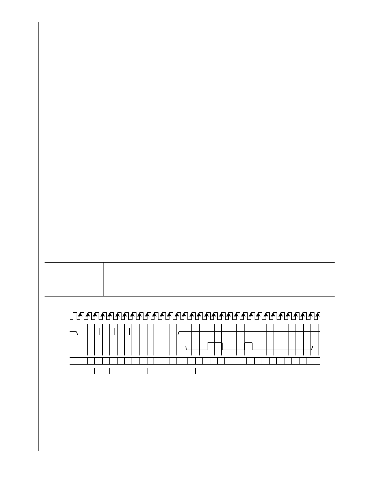
Table 4. Typical MDIO Frame Format
MII Management
<idle><start><op code><device addr><reg addr><turnaround><data><idle>
Serial Protocol
Read Operation <idle><01><10><AAAAA><RRRRR><Z0><xxxx xxxx xxxx xxxx><idle>
Write Operation <idle><01><01><AAAAA><RRRRR><10><xxxx xxxx xxxx xxxx><idle>
MDC
MDIO
(STA)
MDIO
(PHY)
Z
Z
00011 110000000
Idle Start
Opcode
(Read)
PHY Address
(PHYAD = 0Ch)
Register Address
(00h = BMCR)
Z
Z
Z
0 0 011000100000000
TA
Register Data
Figure 2. Typical MDC/MDIO Read Operation
For write transactions, the station management entity
writes data to the addressed DP83847 thus eliminating the
requirement for MDIO Turnaround. The Turnaround time is
filled by the management entity by inserting <10>. Figure 3
shows the timing relationship for a typical MII register write
access.
3.1.3 Serial Management Preamble Suppression
The DP83847 supports a Preamble Suppression mode as
indicated by a one in bit 6 of the Basic Mode Status Register (BMSR, address 01h.) If the station management entity
(i.e. MAC or other management controller) determines that
all PHYs in the system support Preamble Suppression by
Z
Z
Idle
15 www.national.com
Page 16

MDC
DP83847
MDIO
(STA)
Z
00011110000000
Idle Start
Opcode
(Write)
PHY Address
(PHYAD = 0Ch)
Register Address
(00h = BMCR)
Figure 3. Typical MDC/MDIO Write Operation
returning a one in this bit, then the station management
entity need not generate preamble for each management
transaction.
The DP83847 requires a single initialization sequence of
32 bits of preamble foll ow in g ha rdware/software reset. Thi s
requirement is generally met by the mandatory pull-up
resistor on MD I O in co nj unc ti o n wi th a co nt i nuo us MD C, or
the management access made to determine whether Preamble Suppression is supported.
While the DP83847 requires an initial preamble sequence
of 32 bits for management initialization, it does not require
a full 32-bit sequence between each subsequent transaction. A minimum of one idle bit between management
transactions is required as specified in IEEE 802.3u.
3.1.4 PHY Address Sensing
The DP83847 provides five PHY a ddress pins, the inform ation is latched into the PHYCTRL register (address 19h,
bits [4:0]) at device power-up/Hardware reset.
The DP83847 supports PHY Address strapping values 0
( <000 00> ) th rou gh 3 1 ( < 1 1111 > ) . St r a pp ing PHY Address
0 puts the part into Is ola t e Mod e . It should also be noted
that selecting PHY Address 0 via an MDIO write to PHYCTRL will not put the de vice i n Isolat e Mode; Add res s 0 must
be strapped in.
3.1.5 Nibble-wide MII Data Interface
Clause 22 of the IEEE 802.3u specification defines the
Media Independent Interface. This interface includes a
dedicated recei ve bu s an d a dedicated transmi t bus. These
two data buses, alo ng w i th va rio us c ontrol and indicate si gnals, allow for the simultaneous exchange of data between
the DP83847 and the upper layer agent (MAC).
The receive interface consists of a nibble wide data bus
RXD[3:0], a receive error signal RX_ER, a receive data
valid flag RX_DV, and a receive clock RX_CLK for synchronous transfer of the data. The receive clock can operate at either 2.5 MHz to support 10 Mb/s operation modes
or at 25 MHz to support 100 Mb/s operational modes.
The transmit interface consists of a nibble wide data bus
TXD[3:0], a transmit enable control signal TX_EN, and a
transmit cloc k TX_CL K which runs at ei ther 2. 5 MHz or 25
MHz.
Additionally, the MII includes the carrier sense signal CRS,
as well as a collision detect signal COL. The CRS signal
asserts to i ndicate the re ception of d ata from the ne twork
or as a function of transmit data in Half Duplex mode. The
COL signal asse rt s as an ind ic ation of a collision w hi ch ca n
occur during half-duplex operation when both a transmit
and receive operation occur simultaneously.
ZZ
0 0 0 000 00000000
1000
TA
Register Data
3.1.6 Collision Detect
For Half Duplex, a 10BASE-T or 100BASE-TX collision is
detected when the receive and transmit channels are
active sim ultaneously. Collisions ar e reported by the CO L
signal on the MII.
If the DP83847 is tran sm itti ng in 10 M b/s mode when a collision is detected, the collision is not reported until seven
bits have been received while in the collision state. This
prevents a collision being reported incorrectly due to noise
on the network. The COL signal remains set for the duration of the collision.
If a collision occ urs du ring a receive operation, it is immediately reported by the COL signal.
When heartbeat is enabled (only applicable to 10 Mb/s
operation), approximately 1µs after the transmission of
each packet, a Si gn al Q u ali ty Error (SQE) signal o f ap prox imately 10 bit times is generated (internally) to indicate
successful transmiss io n. SQ E is repo rted as a pul se on th e
COL signal of the MII.
3.1.7 Carrier Sense
Carrier Sense (CRS) may be ass ert ed due to receive activity, once valid data is de tec ted v ia the squ elc h fun ct ion during 10 Mb/s operation. During 100 Mb/s operation CRS is
asserted when a valid link (SD) and two non-contiguous
zeros are detected on the line.
For 10 or 100 Mb/s Half Duple x op era tio n, C RS is a sserted
during either packet transmission or reception.
For 10 or 100 Mb/s Full Duplex operation, CRS is asserted
only due to receive activity.
CRS is deasserted following an end of packet.
3.2 100BASE-TX TRANSMITTER
The 100BASE-TX transmitter consists of several functional
blocks which convert sync hronous 4-bit ni bble da t a, as p rovided by the MII, to a scrambled MLT-3 125 Mb/s serial
data stream. Because the 100BASE-TX TP-PMD is integrated, the differential output pins, TD±, can be directly
routed to the magnetics.
The block diagram in Figure 5 provides an overview of
each functional block within the 100BASE-TX transmit section.
The Transmitter section consists of the following functional
blocks:
— Code-group Encoder and Injecti on block ( bypass optio n)
— Scrambler block (bypass option)
— NRZ to NRZI encoder block
— Binary to MLT-3 converter / Common Driver
Z
Idle
16 www.national.com
Page 17
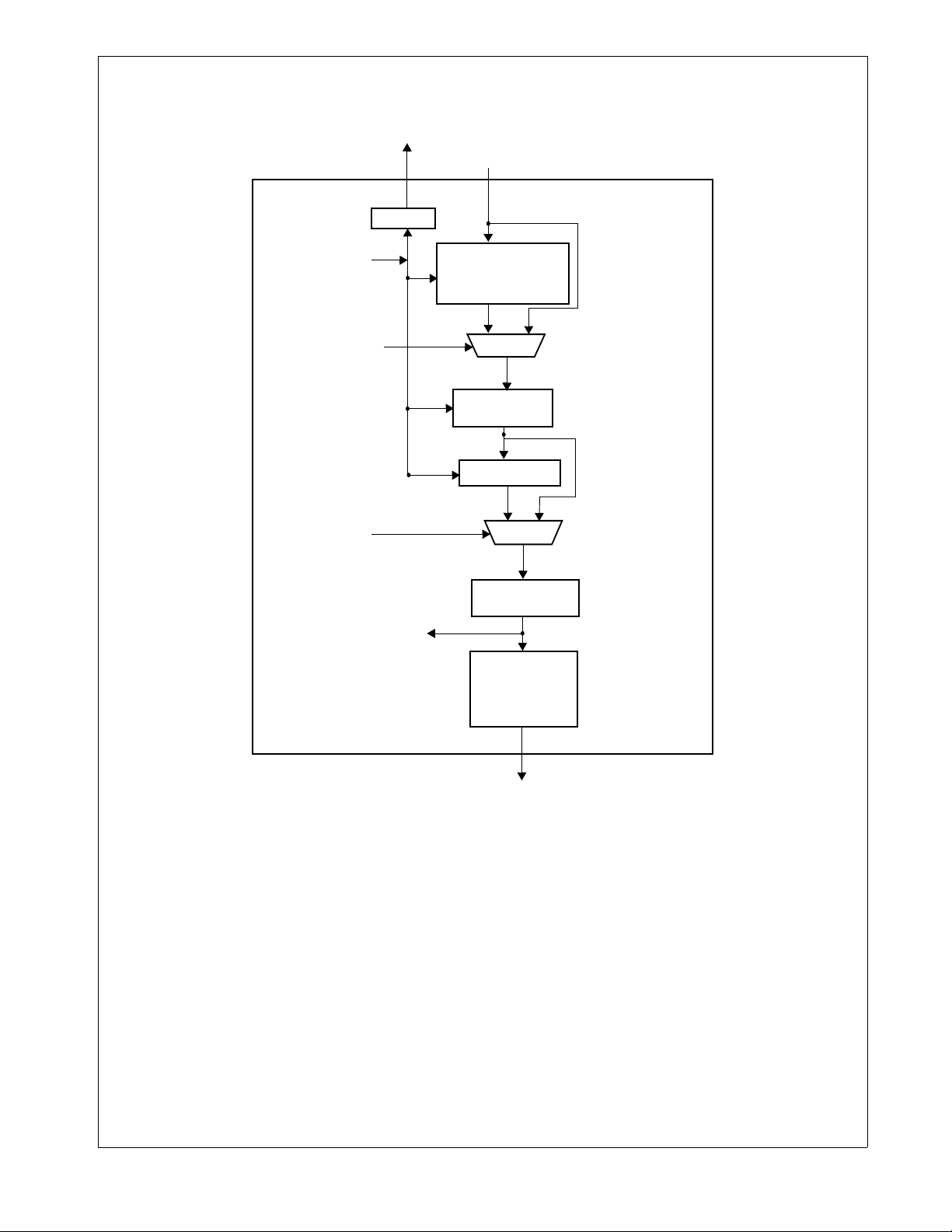
The bypass option for the functional blocks within the
100BASE-TX transmitter provides flexibility for applications
where data conversion is not always required. The
TX_CLK
TXD[3:0] /
DIV BY 5
DP83847
DP83847 implements the 100BASE-TX transmit state
machine diagram as specified in the IEEE 802.3u Standard, Clause 24.
TX_ER
FROM PGM
BP_4B5B
BP_SCR
100BASE-TX
LOOPBACK
4B5B CODE-
GROUP ENCODER
& INJECTOR
MUX
5B PARALLEL
TO SERIAL
SCRAMBLER
MUX
NRZ TO NRZI
ENCODER
BINARY TO
MLT-3 /
COMMON
DRIVER
Figure 4. 100BASE-TX Transmit Block Diagram
3.2.1 Code-group Encoding and Injection
The code-group encoder converts 4-bit (4B) nibble data
generated by the MAC into 5-bit (5B) code-groups for
transmission. This conversion is required to allow control
data to be combined with packet data code-groups. Refer
to T able 5: 4B5B Code-Group Encoding/Decoding for 4B to
5B code-group mapping details.
The code-group encoder substitutes the first 8-bits of the
MAC preamble with a J/K code-group pair (11000 10001)
upon transmission. The code-group encoder continues to
replace subsequent 4B preamble and data nibbles with
corresponding 5B code-groups. At the end of the transmit
packet, upon the deassertion of Transmit Enable signal
from the MAC, the code-group encoder injects the T/R
code-group pair (01101 00111) indicating the en d o f fra me.
TD±
After the T/R code-group pair, the code-group encoder
continuously injects IDLEs into the transmit data stream
until the next transmit packet is detected (reassertion of
Transmit Enabl e).
3.2.2 Scrambler
The scrambler is required to control the radiated emissions
at the media connector and on the twisted pair cable (for
100BASE-TX applications). By scrambling the data, the
total energy launched onto the cable is randomly distributed over a wide frequency range. Without the scrambler,
energy levels at the PMD and on the cable could peak
beyond FCC limitations at frequencies related to repeating
5B sequences (i.e., continuous transmission of IDLEs).
The scrambler is configured as a closed loop linear feedback shift register (LFSR) with an 11-bit polynomial. The
output of the closed loop LFSR is X-ORd with the serial
17 www.national.com
Page 18

NRZ data from the code-group encoder. The result is a
scrambled data stream with sufficient randomization to
decrease radiated emissions at certain frequencies by as
much as 20 dB. The DP83847 uses the PHY_ID (pins
PHYAD [4:0]) to set a unique seed value.
3.2.3 NRZ to NRZI Encoder
After the transmit data stream has been serialized and
scrambled, the data must be NRZI encoded in order to
comply with the TP-PMD standard for 100BASE-TX transmission over Category-5 Unsheilded twisted pair cable.
DP83847
3.2.4 Binary to MLT-3 Convertor / Common Driver
The Binary to MLT-3 conversion.
18 www.national.com
Page 19

T able 5. 4B5B Code-Group Encoding/Decoding
Name PCS 5B Code-group MII 4B Nibble Code
DATA CODES
0 11110 0000
1 01001 0001
2 10100 0010
3 10101 0011
4 01010 0100
5 01011 0101
6 01110 0110
7 01111 0111
8 10010 1000
9 10011 1001
A 10110 1010
B 10111 1011
C 11010 1100
D 11011 1101
E 11100 1110
F 11101 1111
IDLE AND CONTROL CODES
H 00100 HALT code-group - Error code
I 11111 Inter-Packet IDLE - 0000 (
Note 1)
J 11000 First Start of Packet - 0101 (Note 1)
K 10001 Second Start of Packet - 0101 (Note 1)
T 01101 First End of Packet - 0000 (Note 1)
R 00111 Second End of Packet - 0000 (Note 1)
INVALID CODES
V 00000
V 00001
V 00010
V 00011
V 00101
V 00110
V 01000
V 01100
V 10000
V 11001
Note 1: Control code-groups I, J, K, T and R in data fields will be mapped as invalid codes, together with RX_ER asserted.
DP83847
19 www.national.com
Page 20

The 100BASE-TX MLT-3 signal sourced by the TD± com-
mon driver output pins is slew rate controlled. This should
be considered when selecting AC coupling magnetics to
ensure TP-PMD Standard compliant transition times (3 ns
< Tr < 5 ns).
The 100BASE-TX transmit TP-PMD function within the
DP83847 is capab le o f sour cing only MLT-3 encoded da ta.
Binary output from the TD± outputs is not po ssible in 100
Mb/s mode.
3.3 100BASE-TX RECEIVER
The 100BASE-TX receiver consists of several functional
blocks which convert the scrambled MLT-3 125 Mb/s serial
data stream to synchronous 4-bit nibble data that is provided to the MII. Because the 100BASE-TX TP-PMD is
integrated, the differential input pins, RD±, can be directly
routed from the AC coupling magnetics.
See Figure 7 for a block diagram of the 100BASE-TX
receive function. This provides an overview of each functional block within the 100BASE-TX receive section.
The Receive section consists of the following functional
blocks:
DP83847
—ADC
— Input and BLW Compensation
— Signal Detect
— Digital Adaptive Equalization
— MLT-3 to Binary Decoder
— Clock Recovery Module
— NRZI to NRZ Decoder
— Serial to Parallel
— DESCRAMBLER (bypass option)
— Code Group Alignment
— 4B/5B Decoder (bypass option)
— Link Integrity Monitor
— Bad SSD Detection
The bypass option for the functional blocks within the
100BASE-TX receiver provides flexibility for applications
where data conversion is not always required.
3.3.1 Input and Base Line Wander Compensation
Unlike the DP83223V Twister, the DP83847 requires no
external attenuation circuitry at its receive inputs, RD±. It
accepts TP-PMD compliant waveforms directly, requiring
only a 100Ω termination plus a simple 1:1 transformer.
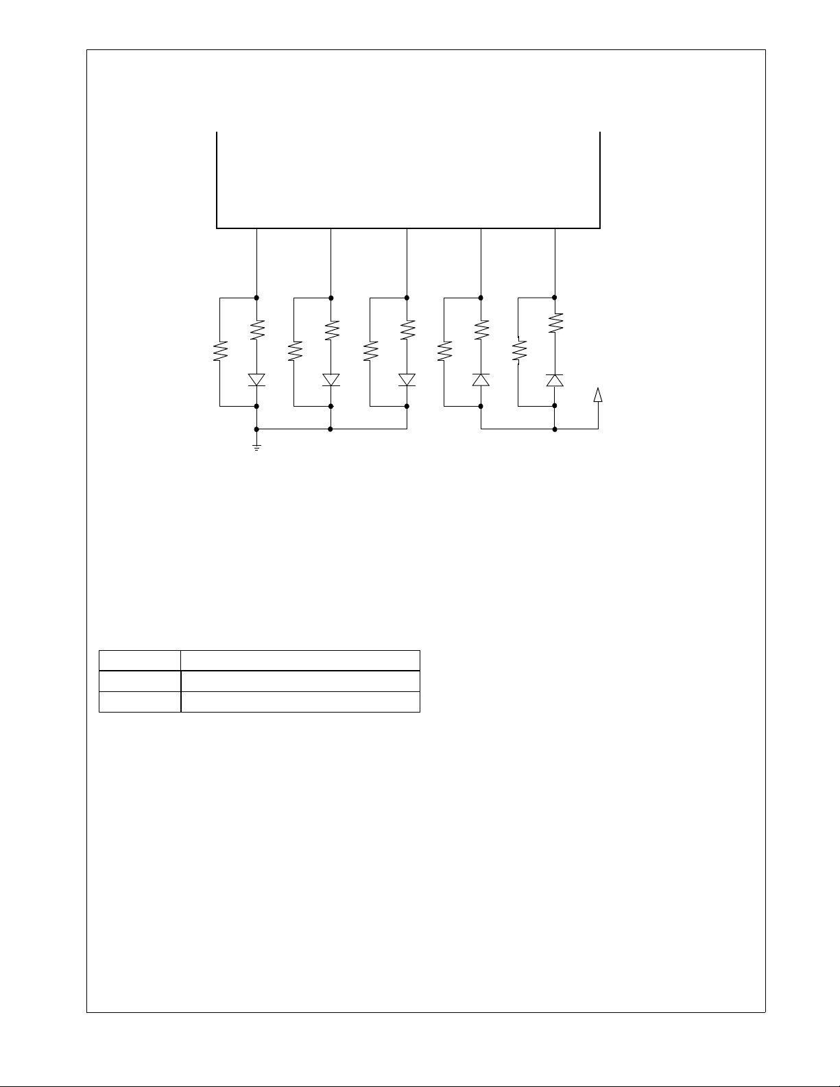
Figure 6. 100BASE-TX BLW Event
The DP83847 is completely ANSI TP-PMD compliant and
includes Base Line Wander (BLW) compensation. The
BLW compensation block can succ e ssf ul ly re c over th e T PPMD defined “killer” pattern and pass it to the digital adaptive equalization block.
BLW can generally be defined as the change in the average DC content, over time, of an AC coupled digital transmission over a given transmission medium. (i.e., copper
wire).
BLW results from the interaction between the low frequency components of a transm itt ed bit stre am and the fre-
quency response of the AC coupling component(s) within
the transmission system. If the low frequency content of
the digital bit stream goes below the low frequency pole of
the AC coupling transformers then the droop characteristics of the transformers will dom in ate res ulting in potentially
serious BLW.
The digital oscilloscope plot provided in Figure 6 illustrates
the severity of the BLW event that can theoretically be generated during 100BASE-TX packet transmission. This
event consists of approximately 800 mV of DC offset for a
20 www.national.com
Page 21

DP83847
RX_CLK
÷5
BP_SCR
BP_4B5B
RXD[3:0] / RX_ER
MUX
4B/5B DECODER
SERIAL TO
PARALLEL
CODE GROUP
ALIGNMENT
MUX
DESCRAMBLER
CLOCK
CLOCK
RECOVERY
MODULE
NRZI TO NRZ
DECODER
MLT-3 TO
BINARY
DECODER
DIGITAL
ADAPTIVE
EQUALIZATION
AGC
INPUT BL W
COMPENSATION
ADC
LINK STATUS
LINK
MONITOR
SIGNAL
DETECT
RD±
Figure 7. Receive Block Diagram
21 www.national.com
Page 22

period of 120 µs. Left uncompensated, events such as this
can cause packet loss.
3.3.2 Signal Detect
The signal detect function of the DP83847 is incorporated
to meet the specificat ion s m an date d by the ANSI FD DI TPPMD Standard as well as the IEEE 802.3 100BASE-TX
Standard for both voltage thresholds and timing parameters.
Note that the reception of normal 10BASE-T link pulses
and fast link pulses per IEEE 802.3u Auto-Negotiation by
the 100BASE-TX receiver do not cause the DP83847 to
assert signal detect.
3.3.3 Digital Adaptive Equaliz ation
When transmitting data at high speeds over copper twisted
pair cable, frequency dependent attenuation becomes a
concern. In high-speed twisted pair signalling, the frequency content of the transmitted signal can vary greatly
during normal operation based primarily on the randomness of the scrambled data stream. This variation in signal
attenuation caused by frequency variations must be compensated for to ensure the integrity of the transmission.
In order to ensure quality transmission when employing
MLT- 3 encoding, the compensati on must be able to ad apt
to various cable lengths and cable types depending on the
installed en vironment. The se lection of lo ng cable lengths
for a given implementation, requires significant compensation which will over-compensate for shorter, less attenuating lengths. Conversely, the selection of short or
intermediate cable lengths requiring less compensation will
cause serious under-compensation for longer length
cables. The compensation or equalization must be adaptive to ensure proper conditioning of the received signal
independent of the cable length.
The DP83847 utilizes a extremely robust equalization
scheme referred as ‘Digital Adaptive Equalization’. Traditional designs use a pseudo adaptive equalization scheme
that determines the approximate cable length by monitoring signal attenuation at certain frequencies. This attenuation value was compared to the internal receive input
reference voltage. This comparison would indicate
amount of equalization to use. Although this scheme is
used successfully on the DP83223V twister, it is sensitive
to transformer mismatch, resistor variation and process
induced offset. The DP83223V also required an external
attenuation network to help match the incoming signal
amplitude to the internal reference.
The Digital Equalizer removes ISI (inter symbol interference) from the receive data stream by continuously adapting to provide a filter with the inverse frequency response
of the channel. When used in conjunction with a gain
stage, this enables the receive 'eye pattern' to be opened
sufficiently to allow very reliable data recovery.
Traditionally 'adaptive' equalizers selected 1 of N filters in
an attempt to match the cables characteristics. This
approach will typically leave holes at certain cable lengths,
where the performance of the equalizer is not optimized.
The DP83847 equalizer is truly adaptive to any length of
cable up to 150m.
3.3.4 Clock Recovery Module
The Clock Recovery Module (CRM) accepts 125 Mb/s
MLT3 data from the equalizer. The DPLL locks onto the
the
DP83847
125 Mb/s data stream and extracts a 125 MHz recovered
clock. The extracted and synchronized clock and data are
used as required by the synchronous receive operations as
generally depicted in Figure 7.
The CRM is implemented using an advanced all digital
Phase Locked Loop (PLL) architecture that replaces sensitive analog circuitry. Using digital PLL circuitry allows the
DP83847 to be manufactured and specified to tighter tolerances.
3.3.5 NRZI to NRZ
In a typical application, the NRZI to NRZ decoder is
required in order to present NRZ formatted data to the
descrambler (or to the code-group alignment block, if the
descrambler is bypassed, or directly to the PCS, if the
receiver i s bypassed).
3.3.6 Serial to Parallel
The 100BASE-TX receiver includes a Serial to Parallel
converter which supplies 5-bit wide data symbols to the
PCS Rx state machine.
3.3.7 Descrambler
A serial descrambler is used to de-scramble the received
NRZ data. The descrambler has to generate an identical
data scrambling sequence (N) in order to recover the original unscrambled data (UD) from the scrambled data (SD)
as represented in the equations:
SD UD N⊕()=
UD SD N⊕()=
Synchronization of the descrambler to the original scrambling sequence (N) is achieved based on the knowledge
that the incoming scrambled data stream consists of
scrambled IDLE data. After the descrambler has recognized 12 consecutive IDLE code-groups, where an
unscrambled IDLE code-group in 5B NRZ is equal to five
consecutive ones (11111), it will synchronize to the receive
data stream and generate unscrambled data in the form of
unaligned 5B code-groups .
In order to maintain synchronization, the descrambler must
continuously monitor the validity of the unscrambled data
that it generates. To ensure this, a line state monitor and a
hold timer are used to constantly monitor the synchronization status. Upon synchronization of the descrambler the
hold timer starts a 722 µs countdown. Upon de tection of
sufficient IDLE c ode -grou p s (58 b it tim es) with in th e 72 2 µs
period, the hold timer will reset and begin a new countdown. This monitoring operation will continue indefinitely
given a properly operating network connection with good
signal integrity. If the line state monitor does not recognize
sufficient unscrambled ID LE code-groups within the 722 µs
period, the entire descrambler will be forced out of the current state of synchronization and reset in order to reacquire synchronization.
3.3.8 Code-group Alignment
The code-group alignment module operates on unaligned
5-bit data from the descrambler (or, if the descrambler is
bypassed, directly from the NRZI/NRZ decoder) and converts it into 5B code-group data (5 bits). Code-group alignment occurs after the J/K code-group pair is detected.
Once the J/K code-group pair (11000 10001) is detected,
subsequent data is aligned on a fixed boundary.
22 www.national.com
Page 23

3.3.9 4B/5B Decoder
The code-group decoder functions as a look up table that
translates incoming 5B code-groups into 4B nibbles. The
code-group decoder first detects the J/K code-group pair
preceded by IDLE code-groups and replaces the J/K with
MAC preamble. Specifically, the J/K 10-bit code-group pair
is replaced by the nibble pair (0101 0101). All subsequent
5B code-groups are converted to the corresponding 4B
nibbles for the duration of the entire packet. This conversion ceases upon the detection of the T/R code-group pair
denoting the End of Stream Delimiter (ESD) or with the
reception of a minimum of two IDLE code-groups.
3.3.10 100BASE-TX Link Integrity Monitor
The 100 Base TX Lin k monito r ensu res tha t a val id and st able link is established before enabling both the Transmit
and Receive PCS layer.
Signal detect must be valid for 395us to allow the link monitor to enter the 'Lin k Up ' s tate, and enable t he t r ans m it an d
receive functions.
3.3.11 Bad SSD Detection
A Bad Start of Stream Delimiter (Bad SSD) is any transition
from consecutive idle code-groups to non-idle code-groups
which is not prefixed by the code-group pair /J/K.
If this condition is detected, the DP83847 will assert
RX_ER and present RXD[3:0] = 1110 to the MII for the
cycles that correspond to received 5B code-groups until at
least two IDLE code groups are detected. In addition, the
False Carrier Sense Counter register (FCSCR) will be
incremented by one.
Once at least tw o IDLE co de groups a re detec ted, RX _ER
and CRS become de-asserted.
3.4 10BASE-T TRANSCEIVER MODULE
The 10BASE-T Transceiver Module is IEEE 802.3 compliant. It includes the receiver, transmitter, collision, heartbeat, loopback, jabber, and link integrity functions, as
defined in the standard. An external filter is not required on
the 10BASE-T interface since this is integrated inside the
DP83847. This section focuses on the general 10BASE-T
system level operation.
3.4.1 Operational Modes
The DP83847 has two basic 10BASE-T operational
modes:
— Half Duplex mode
— Full Duplex mode
Half Duplex Mode
In Half Duplex mode the DP83847 functions as a standard
IEEE 802.3 10BASE-T transceiver supporting the
CSMA/CD protocol.
Full Duplex Mode
In Full Duplex mode the DP83847 is capable of simultaneously transmitting and receiving without asserting the
collision signal. The DP83847's 10 Mb/s ENDEC is
designed to encode and decode simultaneously.
DP83847
3.4.2 Collision Detection and SQE
When in Half Duplex, a 10BASE-T collision is detected
when the receive and transmit channels are active simultaneously. Collisions are reported by the COL signal on the
MII. Collisions are also reported when a jabber condition is
detected.
The COL signal remain s set for the d uration of the c ollis ion.
If the ENDEC is receiving when a collision is detected it is
reported immediately (through the COL pin).
When heartbeat is enabled, approximately 1 µs after the
transmission of each packet, a Signal Quality Error (SQE)
signal of approximately 10-bit times is generated to indicate succes sful transmis sion. SQE is re ported as a p ulse
on the COL signal of the MII.
The SQE test is inhibited when the PH Y is set in ful l dup le x
mode. SQE can also be inhibited by setting the
HEARTBEAT_DIS bit in the 10BTSCR register.
3.4.3 Carrier Sense
Carrier Sense (CRS) may be ass ert ed due to receive activity once valid data is detected via the squelch function.
For 10 Mb/s Half Duplex operation, CRS is asserted during
either packet transmission or reception.
For 10 Mb/s Full Duplex operation, CRS is asserted only
during receive activity.
CRS is deasserted following an end of packet.
3.4.4 Normal Link Pulse Detection/Generation
The link pulse generator produces pulses as defined in the
IEEE 802.3 10BASE-T standard. Each link pulse is nominally 100 ns in duration and transmitted every 16 ms in the
absence of transmit data.
Link pulses are used to check the integrity of the connection with the remote end. If valid link pulses are not
received, the link detector disables the 10BASE-T twisted
pair transmitter, receiver and collision detection functions.
When the link integrity function is disabled
(FORCE_LINK_10 of the 10BTSCR register), good link is
forced and the 10BASE-T transceiver will operate regardless of the presence of link pulses.
3.4.5 Jabber Function
The jabber function monitors the DP83847's output and
disables the transmitte r if it atte mp ts to transmit a packe t of
longer than legal s ize. A ja bber timer monitors th e t rans mi tter and disables the transmission if the transmitter is active
beyond the Jab time (20-150 ms).
Once disabled by the Jabber function, the transmitter stays
disabled for the entire time that the ENDEC module's internal transmit enable is asserted. This signal has to be deasserted for approximately 250-750 ms (the “unjab” time)
before the Jabber function re-enables the transmit outputs.
The Jabber function is only relevant in 10BASE-T mode.
3.4.6 Automatic Link Polarity Detection and Correcti on
The DP83847's 10BASE-T transceiver module incorporates an automatic link polarity detection circuit. When
seven consecutive inverted link pulses are received,
inverted polarity is reported.
23 www.national.com
Page 24

A polarity reversal can be cau sed by a wiring error at either
end of the cable, usually at the Main Distribution Frame
(MDF) or patch panel in the wiring closet.
The inverse polarity condition is latched in the 10BTSCR
register. The DP83847's 10BASE-T transceiver module
corrects for this error internally and will continue to decode
received data correctly. This eliminates the need to correct
the wiring error immediately.
The user is cautioned that if Auto Polarity Detection and
Correction is disabled and inverted Polarity is detected but
not corrected, the DsPHYTER may falsely report Good
Link status and allow Transmission and Reception of
inverted data. It is recommended that Auto Polarity Detection and Correction not be disabled during normal operation.
3.4.7 Transmit and Receive Filtering
External 10BASE-T filters are not required when using the
DP83847, as the required signal conditioning is integrated
into the device.
Only isolation/step-up transformers and impedance matching resistors are required for the 10BASE-T transmit and
receive interface. The internal transmit filtering ensures
that all the harmonics in the transmit signal are attenuated
by at least 30 dB.
3.4.8 Transmitter
The encoder begins operation when the Transmit Enable
input (TX_EN) goes high and converts NRZ data to preemphasized Manchester data for the transceiver. For the
duration of TX_EN, the serialized Transmit Data (TXD) is
encoded for the transmit-driver pair (TD±). TXD must be
valid on the rising edge of Transmit Clock (TX_CLK).
DP83847
Transmission ends when TX_EN deasserts. The last transition is always pos itive ; it oc curs a t the cente r of the b it cel l
if the last bit is a one, or at the end of the bit cell if the last
bit is a zero.
3.4.9 Receiver
The decoder consists of a differential rece iv er and a PLL to
separate a Manch ester encoded da ta stream into intern al
clock signals and dat a . The differential inp ut mu st be externally terminated with a differential 100Ω termination network to accommodate UTP cable. The impedance of RD±
(typically 1.1KΩ) is in parallel with the two 54.9Ω resistors
as is shown in Figure 8 below to approximate the 100Ω
termination.
The decoder detect s the end of a frame when no additiona l
mid-bit transitions are detected. Within one and a half bit
times after the last bit, carrier sense is de-asserted.
3.5 TPI Network Circuit
Figure 8 shows the recommended circuit for a 10/100 Mb/s
twisted pair interface. Below is a partial list of recommended transformers. Is is important that the user realize
that variations with PCB and component characteristics
requires that the application be tested to ensure that the
circuit meets the requirements of the intended application.
Pulse PE-68515
Pulse PE-68515L
Pulse H1012B
Halo TG22-S052ND
Valor PT4171
BELFUSE S558-5999-K2
BELFUSE S558-5999-46
RD-
RD+
TD-
TD+
0.1µF*
Vdd
0.1µF*
49.9Ω
54.9Ω
54.9
Ω
49.9 Ω
TRANSFORMER CENTER
0.1µF
Figure 8. 10/100 Mb/s Twisted Pair Interface
COMMON MODE CHOKES
MAY BE REQUIRED.
1:1
T1
1:1
* PLACE CAPACITORS
CLOSE TO THE
TAPS
RDRD+
TDTD+
RJ45
24 www.national.com
Page 25

3.6 ESD Protection
Typically, ESD precautions are predominantly in effect
when handling the devices or board before being installed
in a system. In th os e ca ses, st ri ct ha ndl in g p roc ed u res can
be implemented during the manufacturing process to
greatly reduce the occurrences of catastrophic ESD
events. After the system is assembled, internal components are usually relatively immune from ESD events.
In the case of an installed Ethernet system however, the
network interface pins are still susceptible to external ESD
events. For example, a category 5 cable being dragged
across a carpet has the potential of developing a charge
well above the typical ESD rating of a semiconductor
device.
DP83847 10/100
Vcc
DP83847
For applications where high reliability is required, it is recommended that addition al ESD pro tectio n diode s be added
as shown below. There are numerous dual series connected diode pairs that are available specifically for ESD
protection. The lev el o f pro tec tio n w il l vary dep endent upon
the diode ratings. The primary parameter that affects the
level of ESD protection i s p eak forwa rd su rge current. T yp ical specifications for diodes intended for ESD protection
range from 500mA (Moto rola BAV99LT1 singl e pair diodes)
to 12A (STM DA108S1 Quad pair array). The user should
also select diodes with low input capacitance to minimize
the effect on system performance.
Since performance is dependent upon components used,
board impedance characteristics, and layout, the circuit
should be completely tested to ensure performance to the
required levels.
3.3V Vcc
RJ-45
TX±
RX±
DIODES PLACED
ON THE DEVICE
SIDE OF THE
ISOLATION
TRANSFORMER
PIN 1
PIN 2
Vcc
PIN 3
PIN 6
Figure 9. Typical DP83847 Network Interface with additional ESD protection
25 www.national.com
Page 26

3.7 Crystal Oscillator Circuit
The DsPHYTER II supports an external CMOS level oscillator source or a crystal resonator device. If an external
clock source is us ed , X1 sh ou l d be t i ed to t he cl oc k sou r ce
and X2 should be left floating. In either case, the clock
source must be a 25 MHz 0.0 05% (50 PPM ) CMOS osc illator or a 25 MHz (50 PPM), paral lel , 20 pF lo ad c rys tal resonator. Figure 10 below shows a typical connection for a
crystal reso nator circuit. The load capacitor values will vary
with the crystal vendors; check with the vendor for the recommended lo ads.
The oscillator circuit was designed to drive a parallel resonance AT cut crystal with a minimum drive level of 500µW
and a maximum of 1mW. If a crystal is specified for a lower
drive level, a current limiting resistor should be placed in
series between X2 and the crystal.
As a starting p oint fo r evalua ting an oscilla tor circ uit, if the
requirements for the crystal are not known, C
should be set at 22 pF, and R1 should be set at 0Ω.
L1
and C
L2
DP83847
3.8 Reference Bypass Couple
To ensure correct operation for the DP83847, parallel caps
with values of 10 µF (Tantalum preferred) and .1 µF should
be placed close to pin 42 (C1) of the device. See Figure11
below for proper use of caps.
Pin 42 (C1)
.1 µF10 µF
Figure 11. Reference Bypass Couple
X1
C
L1
Figure 10. Crystal Oscillator Circuit
X2
R
1
C
L2
4.0 Reset Operatio n
The DP83847 can be reset either by hardware or software.
A hardware reset may be accomplished by asserting the
RESET pin after powering up the device (this is required)
or during normal operation when a reset is needed. A software reset is accomplished by setting the reset bit in the
Basic Mode Control regist er.
While either the hardware or software reset can be implemented at any time after device initialization, a hardware
reset, as described in Section 4.1 must be provided upon
device power-up/initialization. Omitting the hardware reset
operation during the device power-up/initialization
sequence can result in improper device operation.
4.1 Hardware Reset
A hardware reset is accomplished by applying a low pulse
(TTL level), with a duration of at least 160 µs, to the
RESET pin during normal operation. This will reset the
device such that all registers will be reset to default values
and the hardware configuration values will be re-latched
into the device (similar to the power-up/reset operation).
4.2 Software Reset
A software reset is accomplished by setting the reset bit
(bit 15) of the Basic Mode Control Register (BMCR). The
period from the point in time when the reset bit is set to the
point in time when software reset has concluded is approximately 160 µs.
The software reset will reset the device such that all registers will be reset to defau lt v alu es and the h ardw a re co nfi guration values will be re-latched into the device (similar to
the power-up/reset operati on). Software dr iver code should
wait 500 µs following a software reset before allowing further serial MII operations with the DP83847.
26 www.national.com
Page 27

5.0 Register Block
Table 6. Register Map
Offset
Hex Decimal
00h 0 RW BMCR Basic Mode Control Register
01h 1 RO BMSR Basic Mode Status Register
02h 2 RO PHYIDR1 PHY Identifier Register #1
03h 3 RO PHYIDR2 PHY Identifier Register #2
04h 4 RW ANAR Auto-Negotiation Advertisement Register
05h 5 RW ANLPAR Auto-Negotiation Link Partner Ability Register (Base Page)
05h 5 RW ANLPARNP Auto-Negotiation Link Partner Ability Register (Next Page)
06h 6 RW ANER Auto-Negotiation Expansion Register
07h 7 RW ANNPTR Auto-Negotiation Next Page TX
08h-Fh 8-15 RESERVED RESERVED
10h 16 RO PHYSTS PHY Status Register
11h-13h 17-19 RESERVED RESERVED
14h 20 RW FCSCR False Carrier Sense Counter Register
15h 21 RW RECR Receive Error Counter Register
16h 22 RW PCSR PCS Sub-Layer Configuration and Status Register
17h 23 RW RESERVED RESERVED
18h 24 RW RESERVED RESERVED
19h 25 RW PHYCTRL PHY Control Register
1Ah 26 RW 10BTSCR 10Base-T Status/Control Register
1Bh 27 RW CDCTRL CD Test Control Register
1Ch-1Fh 28 RW RESERVED RESERVED
Access Tag Description
Extended Registers
DP83847
27 www.national.com
Page 28

Register Name Addr Tag Bit 15 Bit 14 Bit 13 Bit 12 Bit 11 Bit 10 Bit 9 Bit 8 Bit 7 Bit 6 Bit 5 Bit 4 Bit 3 Bit 2 Bit 1 Bit 0
Basic Mode Control Register
Basic Mode Status Register
PHY Identifier Register 1
PHY Identifier Register 2
Auto-Negotiation Advertisement Register
Auto-Negotiation Link Partner Ability Register (Base Page)
Auto-Negotiation Link Partner Ability Register Next Page
Auto-Negotiation Expansion Register
Auto-Negotiation Next Page TX Register
RESERVED
28 www.national.com
PHY Status Register
00h BM CR Reset Loopback Speed Se-
01h BMSR 100Base-T4100Base-
02h PHYIDR1 OUI MSB OUI MSB OUI MSB OUI MSB OUI MSB OUI MSB OUI MSB OUI MSB OUI MSB OUI MSB OUI MSB OUI MSB OUI MSB OUI MSB OUI MSB OUI MSB
03h PHYIDR2 OUI LSB OUI LSB OUI LSB OUI LSB OUI LSB OUI LSB VNDR_
04h ANA R Next Page
05h ANLP AR Next Page
05h ANLP ARNP Next Page
06h ANER Reserved Reserved Reserved Reserved Reserved Reserved Reserved Reserved Reserved Reserved Reserved PDF LP_NP_
07h ANN PTR Next Page
08-0fh Reserved Reserved Reserved Reserved Reserved Reserved Reserved Reserved Reserved Reserved Reserved Reserved R eserved Reserved Reserved Reserved Reserved
Ind
Ind
Ind
Ind
TX FDX
Reserved Remote
ACK Remote
ACK Message
Reserved Message
Auto-Neg
lect
100Base-
10Base-
TX HDX
Reserved Reserved PAUSE T4 TX_FD TX 10_FD 10 Protocol
Fault
Reserved Reserved Reserved T4 TX_FD TX 10_FD 10 Protocol
Fault
Page
Page
Power
Enable
10Base-
T
FDX
ACK2 Toggle Code Code Code Code Code Code Code Code Code Code Code
ACK2 TOG_TX CODE CODE CODE CODE CODE CODE CODE CODE CODE CODE CODE
Isolate Restart
down
HDX
T
Auto-Neg
Reserved Reserved Reserved Reserved MF Pre-
MDL
Duplex Collision
VNDR_
MDL
Test
VNDR_
MDL
Reserved Reserved Reserved Reserved Reserved Reserved Reserved
amble
Suppress
VNDR_
MDL
Auto-Neg
Complete
VNDR_
MDL
Remote
Fault
VNDR_
MDL
Selection
Selection
Auto-Neg
Ability
MDL_
REV
Protocol
Selection
Protocol
Selection
ABLE
Link
Status
MDL_
REV
Protocol
Selection
Protocol
Selection
NP_
ABLE
Jabber
Extended
Detect
Capability
MDL_
MDL_
REV
REV
Protocol
Selection
Selection
Protocol
Selection
Protocol
Protocol
Selection
PAGE_RXLP_AN_
ABLE
EXTENDED REGISTERS
10h PHY S TS Reserved Reserved Rx Err
Latch
Polarity
Status
False Carrier Sense
Signal De-
tect
Descram
Lock
Page
Receive
Reserved Remote
Fault
Jabber
Detect
Auto-Neg
Complete
Loopback
Status
Duplex
Status
Speed
Status
DP83847
Page 29

5.1 Register Definition
In the register definitions under the ‘Default’ heading, the following definitions hold true:
— RW=Read Write access
— SC=Register sets on event occurrence and Self-Clears when event ends
— RW/SC =Read Write access/Self Clearing bit
— RO=Read Only access
— COR = Clear on Read
— RO/COR=Read Only, Clear on Read
— RO/P=Read Only, Permanently set to a default value
— LL=Latched Low and held until read, based upon the occurrence of the corresponding event
— LH=Latched High and held until read, based upon the occurrence of the corresponding event
DP83847
29 www.national.com
Page 30

Table 7. Basic Mode Control Register (BMCR), Address 0x00
Bit Bit Name Default Description
15 Reset 0, RW/SC Reset:
1 = Initiate software Reset / Reset in Process.
0 = Normal operation.
This bit, which is self-clearing, returns a value of one until the reset process is
complete. The configuration is re-strapped.
14 Loopback 0, RW Loopback:
1 = Loopback enabled.
0 = Normal operation.
The loopback function enables MII transmit data to be routed to the MII receive
data path.
Setting this bit may cause the desc rambler to lose sy nchronizati on and produce a
500 µs “dead time” before any valid data will appear at the MII receive outputs.
13 Speed Selection Strap, RW Speed Select:
When auto-negotiatio n is disabled writing to th is bit allo ws the port spe ed to be selected.
1 = 100 Mb/s.
0 = 10 Mb/s.
12 Auto-Negotiation
Enable
11 Power Down 0, RW Power Down:
10 Isolate 0, RW Isolate:
9 Restart Auto-
Negotiation
8 Duplex Mode St rap, RW Duplex Mode:
Strap, RW Auto-Negotiation Enable:
Strap controls initial value at reset.
1 = Auto-Negotiation Enabled - bits 8 and 13 of this register are ig nored when this
bit is set.
0 = Auto-Negotiation Disa bled - bits 8 and 13 determi ne the port speed and dupl ex
mode.
1 = Power down.
0 = Normal operation.
Setting this bit powers down th e PHY. Only the regis ter block is enable d during a
power down condition.
1 = Isolates the Port from the MII with the exception of the serial management.
0 = Normal operation.
0, RW/SC Restart Auto-Negotiation:
1 = Restart Auto-Negotiation. Re-initiates the Auto-Negotiation process. If AutoNegotiation is disa ble d (b it 12 = 0), this bit is ig nored. This bit is sel f-c lea ring and
will return a value of 1 until Auto-Negotiation is initiated, whereupon it will selfclear. Operation of the Auto-Negotiation process is not affected by the management entity clearing this bit.
0 = Normal operation.
When auto-negotiation is disabled writing to this bit allows the port Duplex capability to be selected.
DP83847
30 www.national.com
Page 31

Table 8. Basic Mode Status Register (BMSR), address 0x01
Bit Bit Name De fault Description
15 100BASE-T4 0, RO/P 100BASE-T4 Capable:
0 = Device not able to perform 100BASE-T4 mode.
14 100BASE-TX
Full Duplex
13 100BASE-TX
Half Duplex
12 10BASE-T
Full Duplex
11 10BASE-T
Half Duplex
10:7 RESERVED 0, RO RESERVED: Write as 0, read as 0.
6MF Preamble
Suppression
5 Auto-Negotiation
Complete
4 Remote Fault 0, RO/LH Remote Fault:
3 Auto-Negotiation
Ability
2 Link Status 0, RO/LL Link Status:
1 Jabber Detect 0, RO/LH Jabber Detect: This bit only has meaning in 10 Mb/s mode.
0 Extended Capabili-
ty
1, RO/P 100BASE-TX Full Duplex Capable:
1 = Device able to perform 100BASE-TX in full duplex mode.
1, RO/P 1 00BASE-TX Half Duplex Capable:
1 = Device able to perform 100BASE-TX in half duplex mode.
1, RO/P 10BASE-T Full Duplex Capable:
1 = Device able to perform 10BASE-T in full duplex mode.
1, RO/P 10BASE-T Half Duplex Capable:
1 = Device able to perform 10BASE-T in half duplex mode.
1, RO/P Preamble suppression Capable:
1 = Device able to perform management transaction with preamble
suppressed, 32-bits of preamble needed only once after reset, invalid
opcode or invalid turnaround.
0 = Normal management operation.
0, RO Auto-Negotiation Complete:
1 = Auto-Negotiation process complete.
0 = Auto-Negotiation process not complete.
1 = Remote Fault condition detected (cleared on read or by reset).
Fault criteria: Far End Fault Indication or notification from Link Partner of Remote Fault.
0 = No remote fault condition detected.
1, RO/P Auto Negotiation Ability:
1 = Device is able to perform Auto-Negotiation.
0 = Device is not able to perform Auto-Negotiation.
1 = Valid link established (for either 10 or 100 Mb/s operation).
0 = Link not established.
The criteria for link validity is implementation specific. The occurrence
of a link failure conditio n will caus es the Link Stat us bit to clear. Once
cleared, this bit may o nly be s et by esta blish ing a good link con dition
and a read via the management interface.
1 = Jabber condition detected.
0 = No Jabber.
This bit is implemented with a latching function, such that the occur-
rence of a jabber conditio n causes it to se t until it is cleare d by a read
to this register by the management interface or by a reset.
1, RO/P Extended Capability:
1 = Extended register capabilities.
0 = Basic register set capabilities only.
DP83847
31 www.national.com
Page 32

The PHY Identifier Registers #1 and #2 together form a unique identifier for the DP83847. The Identifier consists of a
concatenation of the Organizationally Unique Identifier (OUI), the vendor's model number and the model revision number. A PHY may r etur n a val ue of zero in eac h of th e 32 bi ts of the PHY Identi fier if d esired . The PHY I dentifi er is i ntende d
to support network management. National's IEEE assigned OUI is 080017h.
Table 9. PHY Identifier Register #1 (PHYIDR1), address 0x02
Bit Bit Name Default Description
15:0 OUI_MSB <0010 0000 0000
0000>, RO/P
Table 10. PHY Identifier Register #2 (PHYIDR2), address 0x03
Bit Bit Name Default Description
15:10 OUI_LSB <01 0111>, RO/P OUI Least Significant Bits:
9:4 VNDR_MDL <00 0011>, RO/P Vendor Model Number:
3:0 MDL_REV <0000>, RO/P Model Revision Number:
OUI Most Significant Bits: Bits 3 to 18 of the OUI (080017h) are
stored in bits 15 to 0 of this register. The most significant two bits
of the OUI are ignored (the IEEE stan dard refe rs to these as bit s 1
and 2).
Bits 19 to 24 of the OUI (080017h) are mapped to bits 15 to 10 of
this register respectively.
The six bits of vendor model number are mapped to bits 9 to 4
(most significant bit to bit 9).
Four bits of the vendor model revision number are mapped to bits
3 to 0 (most signifi cant bit to bit 3). This field will b e increment ed for
all major device changes.
DP83847
32 www.national.com
Page 33

This register cont ains the ad vertis ed abi lities of thi s dev ice a s they will b e trans mitted to it s link pa rtne r during Auto-N egotiation.
Table 11. Auto-Negotiation Advertisement Register (ANAR), address 0x04
Bit Bit Name Default Description
15 NP 0, RW Next Page Indication:
0 = Next Page Transfer no t desired.
1 = Next Page Transfer desired.
14 RESERVED 0, RO/P RESERVED by IEEE: Writes ignored, Read as 0.
13 RF 0, RW Remote Fault:
1 = Advertises that this device has detected a Remote Fault.
0 = No Remote Fault detected.
12:11 RESERVED 0, RW RESERVED for Future IEEE use: Write as 0, Read as 0
10 PAUSE Strap, RW PAUSE: The default is set by the strap option for PAUSE_EN
1 = Advertise that the DTE (MAC) has implemented both the op-
tional MAC control su bl ayer an d the p ause fu nctio n as s pecif ied in
clause 31 and annex 31B of 802.3u.
0= No MAC based full duplex flow control.
9 T4 0, RO/P 100BASE-T4 Support:
1= 100BASE-T4 is supported by the local device.
0 = 100BASE-T4 not supported.
8 TX_FD Strap, RW 100BASE-TX Full Duplex Support:
1 = 100BASE-TX Full Duplex is supported by the local device.
0 = 100BASE-TX Full Duplex not supported.
7 TX Strap, RW 100BASE-TX Support:
1 = 100BASE-TX is supported by the local device.
0 = 100BASE-TX not supported.
6 10_FD Strap, RW 10BASE-T Full Duplex Support:
1 = 10BASE-T Full Duplex is supported by the local device.
0 = 10BASE-T Full Duplex not supported.
5 10 Strap, RW 10BASE-T Support:
1 = 10BASE-T is supported by the local device.
0 = 10BASE-T not supported.
4:0 Selector <00001>, RW Protocol Selection Bits:
These bits contain the binary enc oded protoco l se lector s upporte d
by this port. <00001> indicates that this device supports IEEE
802.3u.
pin.
DP83847
33 www.national.com
Page 34

This register contains the advertised abilities of the Link Partner as received during Auto-Negotiation. The content
changes after the successful autonegotiation if Next-pages are supported.
Table 12. Auto-Negotiation Link Partner Ability Register (ANLPAR) (BASE Page), address 0x05
Bit Bit Name Default Description
15 NP 0, RO Next Page Indication:
0 = Link Partner does not desire Next Page Transfer.
1 = Link Partner desires Next Page Transfer.
14 ACK 0, RO Acknowledge:
1 = Link Partner acknowledges reception of the ability data word.
0 = Not acknowledged.
The Device's Auto-Negotiation state machine will automatically
control the this bit based on the incoming FLP bursts.
13 RF 0, RO Remote Fault:
1 = Remote Fault indicated by Link Partner.
0 = No Remote Fault indicated by Link Partner.
12:10 RESERVED 0, RO RESERVED for Future IEEE use:
Write as 0, read as 0.
9T4 0, RO100BASE-T4 Support:
1 = 100BASE-T4 is supported by the Link Partner.
0 = 100BASE-T4 not supported by the Link Partner.
8TX_FD 0, RO100BASE-TX Full Duplex Support:
1 = 100BASE-TX Full Duplex is supported by the Link Partner.
0 = 100BASE-TX Full Duplex not supported by the Link Partner.
7TX 0, RO100BASE-TX Support:
1 = 100BASE-TX is supported by the Link Partner.
0 = 100BASE-TX not supported by the Link Partner.
6 10_FD 0, RO 10BASE-T Full Duplex Support:
1 = 10BASE-T Full Duplex is supported by the Link Partner.
0 = 10BASE-T Full Duplex not supported by the Link Partner.
510 0, RO10BASE-T Support:
1 = 10BASE-T is supported by the Link Partner.
0 = 10BASE-T not supported by the Link Partner.
4:0 Selector <0 0000>, RO Protocol Selection Bits:
Link Partner’s binary encoded protocol selector.
DP83847
34 www.national.com
Page 35

Table 13. Auto-Negotiation Link Partner Ability Register (ANLPAR) Next Page, address 0x05
Bit Bit Name Default Description
15 NP 0, RO Next Page Indication:
1 = Link Partner desires Next Page Transfer.
0 = Link Partner does not desire Next Page Transfer.
14 ACK 0, RO Acknowledge:
1 = Link Partner acknowledges reception of the ability data word.
0 = Not acknowledged.
The Device's Auto-Negotiation state machine will automatically
control the this bit based on the incoming FLP bursts. Software
should not attempt to write to this bit.
13 MP 0, RO Message Page:
1 = Message Page.
0 = Unformatted Page.
12 ACK2 0, RO Acknowledge 2:
1 = Link Partner does have the abi lity to comply to next page mes-
sage.
0 = Link Partner does not have the ability to comply to next page
message.
11 Toggle 0, RO Toggle:
1 = Previous value of the transmitted Link Code word equalled 0.
0 = Previous value of the transmitted Link Code word equalled 1.
10:0 CODE <000 0000 0000>, ROCode:
This field represents the code field of the next page transmission.
If the MP bit is set (bit 13 of this register), then the code shall be
interpreted as a “Message Page”, as defined in annex 28C of
Clause 28. Otherwise, the code shall be interpreted as an “Unfor-
matted Page”, and the interpretation is application specific.
DP83847
This register contains additional Local Device and Link Partner status information.
Table 14. Auto-Negotiate Expansion Register (ANER), address 0x06
Bit Bit Name Default Description
15:5 RESERVED 0, RO RESERVED: Writes ignored, Read as 0.
4 PDF 0, RO Parallel Detection Fault:
1 = A fault has been detected via the Parallel Detection function.
0 = A fault has not been detected.
3 LP_NP_ABLE 0, RO Link Partner Next Page Able:
1 = Link Partner does support Next Page.
0 = Link Partner does not support Next Page.
2 NP_ABLE 1, RO/P Next Page Able:
1 = Indicates local device is able to send additional “Next Pages”.
1 PAGE_RX 0, RO/COR Link Code Word Page Received:
1 = Link Code Word has been received, cleared on a read.
0 = Link Code Word has not been received.
0 LP_AN_ABLE 0, RO Link Partner Auto-Negotiation Able:
1 = indicates that the Link Partner supports Auto-Negotiation.
0 = indicates that the Link Partner does not support Auto-Negotia-
tion.
35 www.national.com
Page 36

This register contains the next page information sent by this device to its Link Partner during Auto-Negotiation.
T a ble 15. Auto-Negotiation Next Page Transmit Register (ANNPTR), address 0x07
Bit Bit Name Default Description
15 NP 0, RW Next Page Indication:
0 = No other Next Page Transfer desired.
1 = Another Next Page desired.
14 RESERVED 0, RO RESERVED: Writes ignored, read as 0.
13 MP 1, RW Message Page:
1 = Message Page.
0 = Unformatted Page.
12 ACK2 0, RW Acknowledge2:
1 = Will comply with message.
0 = Cannot comply with message.
Acknowledge2 is used by the next page func tion to indicate tha t Lo-
cal Device has the ability to comply with the message received.
11 TOG_TX 0, RO Toggle:
1 = Value of toggle bit in previously transmitted Link Code Word
was 0.
0 = Value of toggle bit in previously transmitted Link Code Word
was 1.
Toggle is used by the Arbitration function within Auto-Negotiation
to ensure synchronization with the Link Partner during Next Page
exchange. This bit sh all alwa ys tak e the oppo site va lu e of the Tog -
gle bit in the previously exchanged Link Code Word.
10:0 CODE <000 0000 0001>, RWThis field represents the code field of the next page transmission.
If the MP bit is set (bit 13 of this register), then the code shall be
interpreted as a "Messag e Page”, as de fined in annex 28C of IEEE
802.3u. Otherwise, the code shall be interpreted as an "Unformat-
ted Page”, and the interpretation is application specific.
The default value of the CODE represents a Null Page as defined
in Annex 28C of IEEE 802.3u.
DP83847
36 www.national.com
Page 37

DP83847
37 www.national.com
Page 38

Table 16. PHY Status Register (PHYSTS), address 0x10 (Continued)
Bit Bit Name Default Description
7 RESERVED 0, RO RESERVED: Writes ignored, Read as 0.
6 Remote Fault 0, RO Remote Fault:
1 = Remote Fault c ondition detected (cleared on read of BMSR (address 01h) register or by reset). Fault c riteria: notif ication from Link
Partner of Remote Fault via Auto-Negotiation.
0 = No remote fault condition detected.
5 Jabber Detect 0, RO Jabber Detect: This bit only has meaning in 10 Mb/s mode
This bit is a dupl icate of the Jabber De tect bit in the BMSR register,
except that it is not cleared upon a read of the PHYSTS register.
1 = Jabber condition detected.
0 = No Jabber.
4 Auto-Neg Complete 0, RO Auto-Negotiation Complete:
1 = Auto-Negotiation complete.
0 = Auto-Negotiation not complete.
3 Loopback Status 0, RO Loopback:
1 = Loopback enabled.
0 = Normal operation.
2 Duplex Status 0, RO Duplex:
This bit indicates duplex status and is determ ined from Auto -Negotiation or Forced Modes.
1 = Full duplex mode.
0 = Half duplex mode.
Note: This bit is only valid if Auto-Negotiation is enabled and com-
plete and there is a valid li nk or if Au to-Negoti ation i s disa bled an d
there is a valid link.
1 Speed Status 0, RO Speed10:
This bit indicates the status of the speed and is determined from
Auto-Negotiation or Forced Modes.
1 = 10 Mb/s mode.
0 = 100 Mb/s mode.
Note: This bit is only valid if Auto-Negotiation is enabled and com-
plete and there is a valid li nk or if Au to-Negoti ation i s disa bled an d
there is a valid link.
0 Link Status 0, RO Link Status:
This bit is a duplicate of the Link Status bit in the BMSR register,
except that it will no be cleared upon a read of the PHYSTS register.
1 = Valid link established (for either 10 or 100 Mb/s operation).
0 = Link not established.
DP83847
This counter provides information required to implement the “FalseCarriers” attribute within the MAU managed object
class of Clause 30 of the IEEE 802.3u specification.
Table 17. False Carrier Sense Counter Register (FCSCR), address 0x14
Bit Bit Name Default Description
15:8 RESERVED 0, RO RESERVED: Writes ignored, Read as 0
7:0 FCSCNT[7:0] 0, RW / COR False Carrier Event Counter:
This 8-bit counter increments on every false carrier event. This
counter sticks when it reaches its max count (FFh).
38 www.national.com
Page 39

This counter provides information required to implement
the “SymbolErrorDuringCarrier” attribute within the PHY
Table 18. Receiver Error Counter Register (RECR), address 0x15
Bit Bit Name Default Description
15:8 RESERVED 0, RO RESERVED: Writes ignored, Read as 0
7:0 RXERCNT[7:0] 0, RW / COR RX_ER Counter:
This 8-bit counter increments for each receive error detected.
When a valid car rier is prese nt and there is at leas t one occur rence
of an invalid data symbol. Thi s ev ent can in cre me nt on ly on ce per
valid carrier event. If a collision is present, the attribute will not in-
crement. The counter sticks when it reaches its max count.
Table 19. 100 Mb/s PCS Configuration and Status Register (PCSR), address 0x16
Bit Bit Name Default Description
15:13 RESERVED <00>, RO RESERVED: Writes ignored, Read as 0.
12 BYP_4B5B 0, RW Bypass 4B/5B Encoding:
1 = 4B5B encoder functio ns bypassed.
0 = Normal 4B5B operation.
11 FREE_CLK 0, RW Receive Clock:
1 = RX_CK is free-runni ng.
0 = RX_CK phase adjusted based on alignment.
10 TQ_EN
9 SD FORCE PMA
8 SD_OPTION 1, RW Signal Detect Option:
0, RW
0,RW
100Mbs True Quiet Mode Enable:
1 = Transmit True Quiet Mode.
0 = Normal Transmit Mode.
Signal Detect Force PMA:
1 = Forces Signal Detection in PMA.
0 = Normal SD operation.
1 = Enhanced signal detect algorithm.
0 = Reduced signal detect algorithm.
managed object class of Clause 30 of the IEEE 802.3u
specification.
DP83847
39 www.national.com
Page 40

Table 19. 100 Mb/s PCS Configuration and Status Register (PCSR), address 0x16 (Continued)
Bit Bit Name Default Description
7Unused0,RO
6 RESERVED 0 RESERVED:
Must be zero.
5 FORCE_100_OK 0, RW Force 100Mb/s Good Link:
1 = Forces 100Mb/s Good Link.
0 = Normal 100Mb/s operation.
4 RESERVED 0 RESERVED:
Must be zero.
3 RESERVED 0 RESERVED:
Must be zero.
2 NRZI_BYPASS 0, RW NRZI Bypass Enable:
1 = NRZI Bypass Enabled.
0 = NRZI Bypass Disabled.
1 SCRAM _BYPASS 0, RW Scrambler Bypass Enable:
1 = Scrambler Bypass Enabled.
0 = Scrambler Bypass Disabled.
0 DESCRAM_BYPASS 0, RW Descrambler Bypass Enable:
1 = Descrambler Bypass Enabled.
0 = Descrambler Bypass Disabled.
DP83847
Table 20. Reserved Registers, addresses 0x17, 0x18
Bit Bit Name Default Description
15:0 RESERVED none, RW RESERVED: Must not be written to during normal operation.
40 www.national.com
Page 41

Table 21. PHY Control Register (PHYCTRL), address 0x19
Bit Bit Name Default Description
15:12 Unused 0, RO
11 PSR_15 0, RW BIST Sequence select:
1 = PSR15 selected.
0 = PSR9 selected.
10 BIST_STATUS 0, RO/LL BIST Test Status:
1 = BIST pass.
0 = BIST fail. Latched, cleared by write to BIST_ START bit.
9 BIST_START 0, RW BIST Start:
1 = BIST start.
0 = BIST stop.
8 BP_STRETCH 0, RW Bypass LED Stretching:
This will bypass the LED stretching for the Receive, Transmit and
Collision LEDs.
1 = Bypass LED stretching.
0 = Normal operation.
7 PAUSE_STS 0, RO Pause Compare Status:
0 = Local Device and the Link Partner are not Pause capable.
1 = Local Device and the Link Partner are both Pause capable.
6 RESERVED
5 LED_CNFG
4:0 PHYADDR[4:0] Strap, RW PHY Address: PHY address for port.
1, RO/P
Strap, RW
Reserved: Must be 1.
This bit is used to bypass th e selective inversion o n the LED o utput
for DPLX - this enables its use in non-LED applications.
Mode Description
1 = Led polarity adjusted - DPLX selected.
0 = DPLX active HIGH.
DP83847
41 www.national.com
Page 42

Table 22. 10Base-T Status/Control Register (10BTSCR), Address 0x1A
Bit Bit Name Default Description
15:9 Unused 0, RO
8 LOOPBACK_10_DIS 0, RW 10BASE-T Loopback Disable:
If bit 14 (Loopback) in the BMCR is 0:
1 = 10 Mb/s Loopback is disabled.
If bit 14 (Loopback) in the BMCR is 1:
1 = 10 Mb/s Loopback is enabled.
7 LP_DIS 0, RW Normal Link Pulse Disable:
1 = Transmission of NLPs is disabled.
0 = Transmission of NLPs is enabled.
6 FORCE_LINK_10 0, RW Force 10Mb Good Link:
1 = Forced Good 10Mb Link.
0 = Normal Link Status.
5 RESERVED 0, RW RESERVED:
Must be zero.
4POLARITYRO/LH10Mb Polarity Status:
This bit is a duplication of bit 12 in the PHYSTS register. Both bits
will be cleared upon a read of 10BTSCR register, but not upon a
read of the PHYSIS register.
1 = Inverted Polarity detected.
0 = Correct Polarity detected.
3 RESERVED 0, RW RESERVED:
Must be zero.
2 RESERVED 1, RW RESERVED:
Must be set to one.
1 HEARTBEAT_DIS 0, RW Heartbeat Dis able: This bit only has in fluence in half-du plex 10Mb
mode.
1 = Heartbeat function disabled.
0 = Heartbeat function enabled.
When the device is operating at 100Mb or configured for full
duplex operation, this bit will be ignored - the heartbeat function is disabled.
0 JABBER_DIS 0, RW Jabber Disable:
Applicable only in 10BASE-T.
1 = Jabber function disabled.
0 = Jabber function enabled.
DP83847
42 www.national.com
Page 43

DP83847
Table 23. CD Test Register (CDCTRL), Address 0x1B
Bit Bit Name Default Description
15 CD_ENABLE 1, RW CD Enable:
1 = CD Enabled - power-down mode, outputs high impedance.
0 = CD Disabled.
14 DCDCOMP 0, RW Duty Cycle Distortion Compensation:
1 = Increases the amount of DCD compensation.
13 FIL_TTL 0, RW Waveshaper Current Source Test :
To check ability of waveshaper current sources to switch on/off.
1 = Test mode; waveshaping is done, but the output is a square
wave. All sources are either on or off.
0 = Normal mode; sinusoidal.
12 RESERVED none, RW Reserved: This bit should be written with a 0 if write access is re-
11 RISETIME Strap, RW CD Ri10.4(-5.1( T im)9.7(e)38.3( onto)13.7(r)-10.3(o)11.7((:)]TJ/F3 1 Tf-21.6667 -1.6667 TD0.0011 Tc0.0009 Tw[(02)-4296.2(RESERVED)-4090.2(no)10.4(ne,)12.4( RW)]TJ/F4 1 Tf21.6667 0 TD0.0031 Tc0 Tw[(R)5.1(ese)12.4(r)5.4(ved)14.1(: )]TJ/F3 1 Tf5.1067 0 TD0.0035 Tc-0.0015 Tw[(Thi)12.2(s)-3.2( b)12.8(i)-1.2(t )13.3(sho)12.8(u)-0.5(l)12.2(d)-0.5( be)12.8( w)5.5(r)3.2(itt)14.8(en )13.3(w)-7.8(i)12.2(th )13.3(a 0 )13.3(if w)5.5(r)3.2(i)12.2(t)1.5(e a)12.8(c)-3.2(c)10.2(e)-0.5(s)10.2(s)-3.2( )13.3(is )13.3(re-)]TJ-5.1067 -1.1067 TD0.0032 Tc-0.0012 Tw[(qui)11.9(red)12.5( on )13.3(thi)11.9(s)-3.5( re)12.5(gis)9.9(t)1.2(er)16.2(.)]TJ-2138667 -1.6667 TD0.007 Tc0.002 Tw[9D)-93-6.3Fe)-1.3ALsE Strap, RW CDFallnT im.1((e)33( ons)12(t03.7(o((:)]TJ/F3 1 Tf-2138667 -1.6667 TD-0.0020 Tc0.0012 Tw[81)-4310.9CDTESTEND)-9814.90s)915(,)12.2, RW)]TJ/F4 1 Tf2138667 0 TD-0.0015 Tc0.0053 Tw[(CD Tes)-0.8(t)1.2(IM)785(odn )13.3 Enala:
quired on this register.
43 www.national.com
Page 44

6.0 Electrical Specifications
DP83847
Absolute Maximum Ratings
Supply Voltage (V
DC Input Voltage (V
DC Output Voltage (V
Storage Temperature (T
Lead Temp. (TL)
(Soldering, 10 sec)
ESD Rating
= 1.5k, C
(R
ZAP
TPTD+/- ESD Rating
) -0.5 V to 4.2 V
CC
) -0.5V to 5.5V
IN
) -0.5V to 5.5V
OUT
)
STG
= 120 pF)
ZAP
Thermal Characteristic
Theta Junction to Case (T
Theta Junction to Ambient (T
)
jc
) degrees Celsius/Watt - No Airflow @ 1.0W 27.2 °C / W
ja
o
C to 150°C
-65
240 °C
2.0 kV
1.0 kV
Recommended Operating Conditions
Supply voltage (VCC) 3.3 Volts + 0.3V
Ambient Temperature (T
)
A
Max. die temperature (Tj) 150 °C
Max case temp TBD °C
Absolute maximum ratings are those values beyond which
the safety of the device cannot be guaranteed. They are
not meant to imply that the device should be operated at
these limits.
Max Units
3.75 °C / W
Note:0 DC Electrical Specification
Symbol Pin Types Parameter Conditions Min Typ Max Units
V
IH
I/O
I
Input High Voltage Nominal V
CC
1.5 V
0 to 70
°C
V
IL
I
IH
I
IL
V
OL
V
OH
V
ledOL
V
ledOH
I
OZH
I
5IH
I
5OZH
R
INdiff
I
Input Low Voltage 1.1 V
I/O
I
Input High Current VIN = V
I/O
I
Input Low Current VIN = GND -.15 µA
I/O
O,
I/O
O,
I/O
Output Low
Voltage
Output High
Voltage
LED Output Low
Voltage
LED Output High
Voltage
I/O,
O
I/O,
O
I/O,
O
TRI-STATE
Leakage
5 Volt Tolerant
MII Leakage
5 Volt Tolerant
MII Leakage
RD+/− Differential Input
Resistance
CC
1.1 µA
IOL = 4 mA .09 .4 V
IOH = -4 mA Vcc - 0.5 V cc - 0.25 V
* IOL = 2.5 mA .4 V
IOH = -2.5 mA Vcc - 0.5 V
V
OUT
= V
CC
.13 µA
VIN = 5.25 V 5.5 µA
V
= 5.25 V 5.5 µA
OUT
1.2 kΩ
V
TPTD_100
V
TPTDsym
TD+/− 100M Transmit
Voltage
TD+/− 100M Transmit
Voltage Symmetry
.99 V
+/-.5 %
44 www.national.com
Page 45

Symbol Pin Types Parameter Conditions Min Typ Max Units
DP83847
V
TPTD_10
C
IN1
SD
THon
TD+/− 10M Transmit
Voltage
I CMOS Input
Capacitance
RD+/− 100BASE-TX
Signal detect turn-
2.2 2.5 2.8 V
Parameter is not
100% tested
on threshold
SD
THoff
RD+/− 100BASE-TX
Signal detect turnoff threshold
V
TH1
I
dd100
I
dd10
RD+/− 10BASE-T Re-
ceive Threshold
Supply 100BASE-TX
(Full Duplex)
Supply 10BASE-T
(Full Duplex)
I
OUT
See Note
I
OUT
See Note
Note: For Idd Measurements, outputs are not loaded.
= 0 mA
= 0 mA
1pF
295 1000 mV diff
pk-pk
200 mV diff
pk-pk
300 476 585 mV
106 mA
90.5 mA
45 www.national.com
Page 46

6.1 Reset Timing
V
CC
X1 Clock
HARDWARE
RSTN
MDC
Latch-In of Hardware
Configuration Pins
DP83847
T1.0.1
T1.0.4
32 CLOCKS
T1.0.2
T1.0.3
INPUT
Dual Function Pins
Become Enabled As Outputs
Parameter Description Notes Min Typ Max Units
T1.0.1 Post RESET Stabilization time
prior to MDC preamble for register accesses
T1.0.2 Hardware Configuration Latch-
in Time from the Deassertion of
RESET (either soft or hard)
T1.0.3 Hardware Configuration pins
transition to output drivers
T1.0.4 RESET pulse width X1 Clock must be stable for at min. of
Note1: Software Reset should be initiated no sooner then 500 µs after power-up or the deassertion of hardware reset.
Note2: It is important to choose pull-u p and/or pull-down resi stors for each of the hardware co nfiguratio n pins that provide
fast RC time constants in order to latch-in the proper value prior to the pin transitioning to an output driver.
MDIO is pulled h ig h fo r 32 -bi t s eria l ma nagement initializat ion .
Hardware Configuration Pins are described in the Pin Description sec tio n.
160us during RESET pulse low time.
OUTPUT
3 µs
3 µs
3.5 µs
160 µs
46 www.national.com
Page 47

6.2 PGM Clock Timing
X1
TX_CLK
T2.0.1
Parameter Description Notes Min Typ Max Units
T2.0.1 TX_CLK Duty Cycle 35 65 %
6.3 MII Serial Management Timing
DP83847
MDC
T3.0.1
T3.0.4
MDIO (output)
MDC
T3.0.2 T3.0.3
MDIO (input)
Parameter Description Notes Min Typ Max Units
T3.0.1 MDC to MDIO (Output) Delay Time 0 300 ns
T3.0.2 MDIO (Input) to MDC Setup Time 10 ns
T3.0.3 MDIO (Input) to MDC Hold Time 10 ns
T3.0.4 MDC Frequency 2.5 MHz
Valid Data
47 www.national.com
Page 48

6.4 100 Mb/s Timing
6.4.1 100 Mb/s MII Transmit Timing
TX_CLK
DP83847
T4.1.1
TXD[3:0]
TX_EN
TX_ER
Parameter Description Notes Min Typ Max Units
T4.1.1 TXD[3:0], TX_EN, TX_ER Data Setup to
TX_CLK
T4.1.2 TXD[3:0], TX_EN, TX_ER Data Hold from
6.4.2 100 Mb/s MII Receive Timing
RX_CLK
RXD[3:0]
RX_DV
RX_ER
TX_CLK
T4.2.1
T4.2.2
Valid Data
Valid Data
T4.1.2
10 ns
5ns
Parameter Description Notes Min Typ Max Units
T4.2.1 RX_CLK Duty Cycle 35 65 %
T4.2.2 RX_CLK to RXD[3:0], RX_DV, RX_ER Delay 10 30 ns
48 www.national.com
Page 49

6.4.3 100BASE-TX Transmit Packet Latency Timing
TX_CLK
TX_EN
DP83847
TXD
TD±
Parameter Description Notes Min Typ Max Units
T4.3.1 TX_CLK to TD± Latency 6.0 bit times
Note: Latency is determined by measuring the time from the first rising edge of TX_CLK occurring after the assertion of
TX_EN to the first bit of the “J” code group as output from the TD± pins.
6.4.4 100BASE-TX Transmit Packet Deassertion Timing
TX_CLK
TX_EN
T4.3.1
(J/K) IDLE DATA
TXD
TD±
Parameter Description Notes Min Typ Max Units
T4.4.1 TX_CLK to TD± Deassertion 6.0 bit times
Note: Deassertion is determi ned by meas uri ng the time from the firs t ri si ng e dg e of TX_C L K oc cu rrin g after the deassertion of TX_EN to the first bit of the “T” code group as output from the TD± pins.
49 www.national.com
Page 50

6.4.5 100BASE-TX Transmit Timing (t
+1 rise
TD±
T4.5.2
TD±
eye pattern
& Jitter)
R/F
T4.5.1
+1 fall
T4.5.2
T4.5.1
90%
10%
-1 fall
10%
90%
T4.5.1
T4.5.1
-1 rise
DP83847
Parameter Description Notes Min Typ Max Units
T4.5.1 100 Mb/s TD± tR and t
100 Mb/s t
T4.5.2 100 Mb/s TD± Transmit Jitter 1.4 ns
Note1: Normal Mismatch is the difference between the maximum and minimum of all rise and fall times.
Note2: Rise and fall times taken at 10% and 90% of the +1 or -1 amplitude.
and tF Mismatch 500 ps
R
F
345ns
50 www.national.com
Page 51

6.4.6 100BASE-TX Receive Packet Latency Timing
DP83847
RD±
CRS
RXD[3:0]
RX_DV
RX_ER/RXD[4]
Parameter Description Notes Min Typ Max Units
T4.6.1 Carrier Sense ON Delay 17.5 bit times
T4.6.2 Receive Data Latency 21 bit times
Note: Carrier Sense On Delay is de termin ed by meas uring the ti me fro m the first bit of the “J” code group to the asse rtion
of Carrier Sense.
Note: RD± voltage amplitude is greater than the Signal Detect Turn-On Threshold Value.
6.4.7 100BASE-TX Receive Packet Deassertion Timing
IDLE
T4.6.1
(J/K)
Data
T4.6.2
RD±
CRS
RXD[3:0]
RX_DV
RX_ER/RXD[4]
Parameter Description Notes Min Typ Max Units
T4.7.1 Carrier Sense OFF Delay 21.5 bit times
Note: Carrier Sense Off Delay is de termin ed by measu ring th e time from the first b it of the “T” c ode g roup to t he d eassertion of Carrier Sense.
DATA
(T/R)
T4.7.1
IDLE
51 www.national.com
Page 52

6.5 10 Mb/s Timing
6.5.1 10 Mb/s MII Transmit Timing
TX_CLK
DP83847
T5.1.1
TXD[3:0]
TX_EN
Parameter Description Notes Min Typ Max Units
T5.1.1 TXD[3:0], TX_EN Data Setup to TX_CLK 25 ns
T5.1.2 TXD[3:0], TX_EN Data Hold from TX_CLK 5 ns
6.5.2 10 Mb/s MII Receive Timing
T5.2.1
RX_CLK
RXD[3:0]
RX_DV
T5.2.2
Valid Data
Valid Data
T5.1.2
Parameter Description Notes Min Typ Max Units
T5.2.1 RX_CLK Duty Cycle 35 65 %
T5.2.2 RX_CLK to RXD[3:0], RX_DV 190 210 ns
52 www.national.com
Page 53

6.5.3 10BASE-T Transmit Timing (Start of Packet)
TX_CLK
T5.3.1
TX_EN
T5.3.2
DP83847
TXD[0]
TPTD±
Parameter Description Notes Min Typ Max Units
T5.3.1 Transmit Enable Setup Time from the
Falling Edge of TX_CLK
T5.3.2 Transmit Data Setup Time from the
Falling Edge of TX_CLK
T5.3.3 Transmit Data Hold Time from the
Falling Edge of TX_CLK
T5.3.4 Transmit Output Delay from the
Falling Edge of TX_CLK
6.5.4 10BASE-T Transmit Timing (End of Packet)
T5.3.3
T5.3.4
25 ns
25 ns
5ns
6.8 bit times
TX_CLK
T5.4.1
TX_EN
TPTD±
TPTD±
Parameter Description Notes Min Typ Max Units
T5.4.1 Transmit Enable Hold Time f rom the
Falling Edge of TX_CLK
T5.4.2 End of Packet High Time
(with ‘0’ ending bit)
T5.4.3 End of Packet High Time
(with ‘1’ ending bit)
00
11
5ns
250 ns
250 ns
T5.4.2
T5.4.3
53 www.national.com
Page 54

6.5.5 10BASE-T Receive Timing (Start of Packet)
DP83847
1st SFD bit decoded
1
TPRD±
T5.5.1
CRS
T5.5.2
RX_CLK
T5.5.4
RXD[0]
T5.5.3
RX_DV
Parameter Description Notes Min Typ Max Units
T5.5.1 Carrier Sense Turn On Delay
(TPRD± to CRS)
1µs
0
1
T5.5.2 Decoder Acquisition Time 3.6 µs
T5.5.3 Receive Data Latency 17.3 bit times
T5.5.4 SFD Propagation Delay 10 bit times
Note: 10BASE-T receive Data Latency is measured from first bit of preamble on the wire to the assertion of RX_DV.
6.5.6 10BASE-T Receive Timing (End of Packet)
1
TPRD±
RX_CLK
CRS
Parameter Description Notes Min Typ Max Units
T5.6.1 Carrier Sense Turn Off Delay 1.1 µs
0
1
IDLE
T5.6.1
54 www.national.com
Page 55

6.5.7 10 Mb/s Heartbeat Timing
TXE
DP83847
TXC
COL
Parameter Description Notes Min Typ Max Units
T5.7.1 CD Heartbeat Delay 600 1600 ns
T5.7.2 CD Heartbeat Duration 500 1500 ns
6.5.8 10 Mb/s Jabber Timing
TXE
T5.8.1
TPTD±
COL
T5.7.1
T5.7.2
T5.8.2
Parameter Description Notes Min Typ Max Units
T5.8.1 Jabber Activation Time 20 150 ms
T5.8.2 Jabber Deactivation Time 250 750 ms
6.5.9 10BASE-T Normal Link Pulse Timing
T5.9.2
T5.9.1
Normal Link Pulse(s)
Parameter Description Notes Min Typ Max Units
T5.9.1 Pulse Width 100 ns
T5.9.2 Pulse Period 8 16 24 ms
55 www.national.com
Page 56

6.5.10 Auto-Negotiation Fast Link Pulse (FLP) Timing
T5.10.2
T5.10.3
T5.10.1
Fast Link Pulse(s)
DP83847
T5.10.1
clock
pulse
T5.10.4
Parameter Description Notes Min Typ Max Units
T5.10.1 Clock, Data Pulse Width 100 ns
T5.10.2 Clock Pulse to Clock Pulse
Period
T5.10.3 Clock Pulse to Data Pulse
Period
T5.10.4 Number of Pulses in a Burst 17 33 #
T5.10.5 Burst Width 2ms
T5.10.6 FLP Burst to FLP Burst Period 8 24 ms
6.5.11 100BASE-TX Signal Detect Timing
T5.10.5
FLP Burst FLP Burst
data
pulse
T5.10.6
Data = 1 55.5 69.5 µs
clock
pulse
111 125 139 µs
RD±
T5.11.1
T5.11.2
SD+ internal
Parameter Description Notes Min Typ Max Units
T5.11.1 SD Internal Turn-on Time 1 ms
T5.11.2 SD Internal Turn-off Time 300 µs
Note: The signal amplitude at RD± is TP-PMD compliant.
56 www.national.com
Page 57

6.6 Loopback Timing
6.6.1 100 Mb/s Internal Loopback Mode
TX_CLK
TX_EN
TXD[3:0]
DP83847
CRS
RX_CLK
RX_DV
RXD[3:0]
Parameter Description Notes Min Typ Max Units
T6.1.1 TX_EN to RX_DV Loopback 100 Mb/s internal loopback mode 240 ns
Note1: Due to the nature of the descrambler function, all 100BASE-TX Loopback modes will cause an initial “dead-time”
of up to 550 µs during which time no data will be present at the receive MII outputs. The 100BASE-TX timing specified is
based on device delays after the initial 550µs “dead-time”.
Note2: Measurement is made from the first rising edge of TX_CLK after assertion of TX_EN.
T6.1.1
57 www.national.com
Page 58

6.6.2 10 Mb/s Internal Loopback Mode
TX_CLK
TX_EN
TXD[3:0]
DP83847
CRS
RX_CLK
RX_DV
RXD[3:0]
Parameter Description Notes Min Typ Max Units
T6.2.1 TX_EN to RX_DV Loopback 10 Mb/s internal loopback mode 2 µs
Note: Measurement is made from the first falling edge of TX_CLK after assertion of TX_EN.
T6.2.1
58 www.national.com
Page 59

6.7 Isolation Timing
Clear bit 10 of BMCR
(return to normal operation
from Isolate mode)
T7.0.1
H/W or S/W Reset
(with PHYAD = 00000)
T7.0.2
MODE
ISOLATE
Parameter Description Notes Min Typ Max Units
T7.0.1 From software clear of bit 10 in
the BMCR register to the transi-
tion from Isolate to Normal Mode
T7.0.2 From Deassertion of S/W or H/W
Reset to transition from Isolate to
Normal mode
NORMAL
100 µs
500 µs
DP83847
59 www.national.com
Page 60

7.0 Physical Dimensions
DP83847 DsPHYTER II — Single 10/100 Ethernet Transceiver
Leadless Leadframe Package (LLP)
Order Number DP83847 LQA56A
NS Package Number LQA-56A
LIFE SUPPORT POLICY
NATIONAL’S PRODUCTS ARE NOT AUTHORIZED FOR USE AS CRITICAL COMPONENTS IN LIFE SUPPORT
DEVICES OR SYSTEMS WITHOUT THE EXPRESS WRITTEN APPROVAL OF THE PRESIDENT AND GENERAL
COUNSEL OF NATIONAL SEMICONDUCTOR CORPORATION. As used herein:
1. Life support devices or systems are devices or
systems which, (a) are intended for surgical implant
into the body, or (b) support or sustain life, and
whose failure to perform when properly used in
accordance with instructions for use provided in the
2. A critical component is any component of a life
support device or system whose failure to perform
can be reasonably expected to cause the failure of
the life support device or system, or to affect its
safety or effectiveness.
labeling, can be reasonably expected to result in a
significant injury to the user.
National Semiconductor
Corporation
Americas
Tel: 1-800-272-9959
Fax: 1-800-737-7018
Email: support@nsc.com
www.national.com
National Semiconductor
Europe
Fax: +49 (0) 180-530 85 86
Email: europe.support@nsc.com
Deutsch Tel: +49 (0) 69 9508 6208
English Tel: +44 (0) 870 24 0 2171
Francais Tel: +33 (0) 1 41 91 8790
National Semic onductor
Asia Pacific Customer
Response Group
Tel: 65-2544466
Fax: 65-2504466
Email: ap.support@nsc.com
National Semicond uctor
Japan Ltd.
Tel: 81-3-5639-7560
Fax: 81-3-5639-7507
National does not assume any responsibility for use of any circuitry described, no circuit patent licenses are implied and National reserves the right at any time without notice to change said circuitry and specifications.
 Loading...