


DP83843BVJE PHYTER
DP83843BVJE PHYTER
July 1999
General Description
TheDP83843BVJEisafullfeaturePhysicalLayerdevice
withintegratedPMDsublayerstosupportboth10BASE-T
and 100BASE-X Ethernet protocols.
ThisVLSIdeviceisdesignedforeasyimplementationof
10/100Mb/sEthernetLANs.ItinterfacesdirectlytoTwisted
Pairmediathroughanexternaltransformerortofiber
mediaviaindustrystandardelectrical/opticalfiberPMD
transceivers.Thisdevicealsointerfacesdirectlytothe
MAClayerthroughtheIEEE802.3ustandardMediaIndependentInterface(MII),ensuringinteroperabilitybetween
products from different vendors.
TheDP83843isdesignedwithNationalSemiconductor's
advancedCMOSprocess.Itssystemarchitectureisbased
ontheintegrationofseveralofNational'sindustryproven
core technologies:
—IEEE 802.3 ENDEC with AUI/10BASE-T transceiver
module to provide the 10 Mb/s functions
—ClockRecovery/GeneratorModulesfromNational'sFast
Ethernet and FDDI products
—FDDI Stream Cipher scrambler/descrambler for
TP-PMD
—100BASE-Xphysicalcodingsub-layer(PCS)andcontrol
logicthatintegratesthecoremodulesintoadualspeed
Ethernet physical layer controller
—ANSI X3T12 Compliant TP-PMD Transceiver
technology with Baseline Wander (BLW) compensation
Features
—IEEE 802.3 ENDEC with AUI/10BASE-T transceivers
and built-in filters
—IEEE 802.3u 100BASE-TX compatible - directly drives
standard Category 5 UTP, no need for external
100BASE-TX transceiver
—Fully Integrated and fully compliant ANSI X3.263 TP-
PMD physical sublayer which includes adaptive equalization and BLW compensation
—IEEE802.3u100BASE-FXcompatible-connectsdirect-
ly to industry standard Electrical/Optical transceivers
—IEEE 802.3u Auto-Negotiation for automatic speed se-
lection
—IEEE 802.3u compatible Media Independent Interface
(MII) with Serial Management Interface
—Integrated high performance 100 Mb/s clock recovery
circuitry requiring no external filters
—Full Duplex support for 10 and 100 Mb/s data rates
—MII Serial 10 Mb/s mode
—Fully configurable node/switch and 100Mb/s repeater
modes
—Programmableloopbackmodesforflexiblesystemdiag-
nostics
—Flexible LED support
—Single register access to complete PHY status
—MDIO interrupt support
—Individualized scrambler seed for 100BASE-TX applica-
tions using multiple PHYs
—Low power consumption for multi-port applications
—Small footprint 80-pin PQFP package
System Diagram
10 AND/OR 100 Mb/s
ETHERNET MAC OR
100Mb/s REPEATER
CONTROLLER
ThunderLAN® is a registered trademark of Texas Instruments.
TWISTER™ is a trademark of National Semiconductor Corporation.
TRI-STATE
®
is a registered trademark of National Semiconductor Corporation.
© 1999 National Semiconductor Corporation
MII
DP83843
10/100 Mb/s
ETHERNET PHYSICAL LAYER
25 MHz
CLOCK
STATUS
LEDS
10BASE-T or
100BASE-TX
MAGNETICS
100BASE-FX/
AUI
RJ-45
10BASE-T
100BASE-TX
www.national.com
or
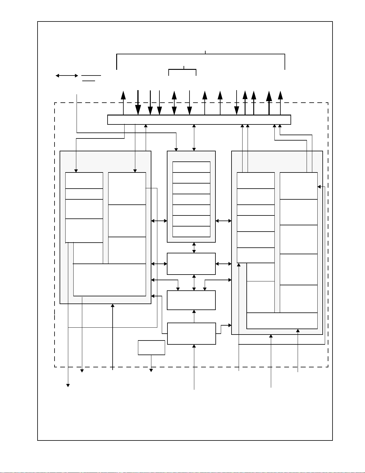
Block Diagram
HARDWARE
CONFIGURATION
PINS
(REPEATER,
SERIAL10, SYMBOL,
,
AN0, AN1,FXEN
PHYAD[4:0])
TX_CLK
TX_ER
TXD[3:0]
MII
SERIAL
MANAGEMENT
TX_EN
MDIO
MII INTERFACE/CONTROL
MDC
COL
CRS
RX_ER
RX_EN
RX_DV
RX_CL
RXD[3:0]
TX_DATA
TRANSMIT CHANNELS &
STATE MACHINES
100 MB/S 10 MB/S
4B/5B
ENCODER
MANCHESTER
SCRAMBLER
PARALLEL TO
SERIAL
NRZ TO NRZI
ENCODER
BINARY TO
MLT-3
ENCODER
10/100 COMMON
OUTPUT DRIVER
TX_DATA
NRZ TO
ENCODER
LINK PULSE
GENERATOR
TRANSMIT
FILTER
TX_CLK
REGISTERS
MII
PHY ADDRESS
AUTO
NEGOTIATION
NODE/RPTR
PCS CONTROL
10BASE-T
100BASE-X
FAR-END-FAULT
STATE MACHINE
AUTO-NEGOTIATION
STATE MACHINE
RX_CLK
DESCRAMBLER
RX_DATA
RECEIVE CHANNELS &
STATE MACHINES
100 MB/S 10 MB/S
4B/5B
DECODER
CODE GROUP
ALIGNMENT
SERIAL TO
PARALLEL
NRZI TO NRZ
DECODER
CLOCK
RECOVERY
MLT-3 TO
BINARY
DECODER
ADAPTIVE
EQ
AND
BLW
COMP.
RX_DATA
RX_CLK
MANCHESTER
TO NRZ
DECODER
CLOCK
RECOVERY
LINK PULSE
DETECTOR
RECEIVE
FILTER
SMART
SQUELCH
FXTD/AUITD+/−
TXAR100
LED
DRIVERS
LEDS
10/100 COMMON
INPUT BUFFER
CLOCK
GENERATION
TPRD+/−TPTD+/−
SYSTEM CLOCK
REFERENCE
FXRD/AUIRD+/−
FXSD/CD+/−
2 www.national.com

Table of Contents
1.0 Pin Descriptions . . . . . . . . . . . . . . . . . . . . . . . . . . . . . . .5
1.1 MII Interface . . . . . . . . . . . . . . . . . . . . . . . . . . . . . .5
1.2 10 Mb/s and 100 Mb/s PMD Interface . . . . . . . . . .6
1.3 Clock Interface . . . . . . . . . . . . . . . . . . . . . . . . . . . .8
1.4 Device Configuration Interface . . . . . . . . . . . . . . .8
1.5 LED Interface . . . . . . . . . . . . . . . . . . . . . . . . . . . .10
1.6 PHY Address Interface . . . . . . . . . . . . . . . . . . . .11
1.7 Reset . . . . . . . . . . . . . . . . . . . . . . . . . . . . . . . . . .11
1.8 Power And Ground Pins . . . . . . . . . . . . . . . . . . .12
1.9 Special Connect Pins . . . . . . . . . . . . . . . . . . . . . .12
2.0 Functional Description . . . . . . . . . . . . . . . . . . . . . . . . .13
2.1 802.3u MII . . . . . . . . . . . . . . . . . . . . . . . . . . . . . .13
2.2 100BASE-TX TRANSMITTER . . . . . . . . . . . . . . .15
2.3 100BASE-TX RECEIVER . . . . . . . . . . . . . . . . . . 18
2.4 10BASE-T TRANSCEIVER MODULE . . . . . . . . .22
2.5 100 BASE-FX . . . . . . . . . . . . . . . . . . . . . . . . . . .24
2.6 AUI . . . . . . . . . . . . . . . . . . . . . . . . . . . . . . . . . . . .26
3.0 Configuration . . . . . . . . . . . . . . . . . . . . . . . . . . . . . . . .28
3.1 Auto-Negotiation . . . . . . . . . . . . . . . . . . . . . . . . . 28
3.2 PHY Address and LEDs . . . . . . . . . . . . . . . . . . .30
3.3 Half Duplex vs. Full Duplex . . . . . . . . . . . . . . . . .31
3.4 100 Mb/s Symbol Mode . . . . . . . . . . . . . . . . . . . . 32
3.5 100BASE-FX Mode . . . . . . . . . . . . . . . . . . . . . . .32
3.6 10 Mb/s Serial Mode . . . . . . . . . . . . . . . . . . . . . .32
3.7 10 Mb/s AUI Mode . . . . . . . . . . . . . . . . . . . . . . . . 32
3.8 Repeater vs. Node . . . . . . . . . . . . . . . . . . . . . . . .33
3.9 Isolate Mode . . . . . . . . . . . . . . . . . . . . . . . . . . . .33
3.10 Loopback . . . . . . . . . . . . . . . . . . . . . . . . . . . . . . .33
4.0 Clock Architecture . . . . . . . . . . . . . . . . . . . . . . . . . . . .34
4.1 Clock Generation Module (CGM) . . . . . . . . . . . .34
4.2 100BASE-X Clock Recovery Module . . . . . . . . . .36
4.3 10 Mb/s Clock Recovery Module . . . . . . . . . . . . . 36
4.4 Reference Clock Connection Options . . . . . . . . .36
5.0 Reset Operation . . . . . . . . . . . . . . . . . . . . . . . . . . . . . . 37
5.1 Power-up / Reset . . . . . . . . . . . . . . . . . . . . . . . . . 37
5.2 Hardware Reset . . . . . . . . . . . . . . . . . . . . . . . . . .37
5.3 Software Reset . . . . . . . . . . . . . . . . . . . . . . . . . .37
6.0 DP83843 Application . . . . . . . . . . . . . . . . . . . . . . . . . .38
6.1 Typical Node Application . . . . . . . . . . . . . . . . . . .38
6.2 Power And Ground Filtering . . . . . . . . . . . . . . . .38
6.3 Power Plane Considerations . . . . . . . . . . . . . . . .38
7.0 User Information . . . . . . . . . . . . . . . . . . . . . . . . . . . . . 42
7.1 Link LED While in Force 100Mb/s Good Link . . . 42
7.2 False Link Indication When in Forced 10Mb/s . . 42
7.3 10Mb/s Repeater Mode . . . . . . . . . . . . . . . . . . . 42
7.4 Resistor Value Modifications . . . . . . . . . . . . . . . 42
7.5 Magnetics . . . . . . . . . . . . . . . . . . . . . . . . . . . . . . 43
7.6 Next Page Toggle Bit Initialization . . . . . . . . . . . 43
7.7 Base Page to Next Page Initial FLP Burst Spacing
43
7.8 100Mb/s FLP Exchange Followed by Quiet . . . . 43
7.9 Common Mode Capacitor for EMI improvement 44
7.10 BAD_SSD Event Lockup . . . . . . . . . . . . . . . . . . 44
8.0 Register Block . . . . . . . . . . . . . . . . . . . . . . . . . . . . . . . 45
8.1 Register Definitions . . . . . . . . . . . . . . . . . . . . . . 45
9.0 Electrical Specifications . . . . . . . . . . . . . . . . . . . . . . . 63
9.1 DC Electrical Specification . . . . . . . . . . . . . . . . . 64
9.2 CGM Clock Timing . . . . . . . . . . . . . . . . . . . . . . 66
9.3 MII Serial Management AC Timing . . . . . . . . . . 66
9.4 100 Mb/s AC Timing . . . . . . . . . . . . . . . . . . . . . . 67
9.5 10 Mb/s AC Timing . . . . . . . . . . . . . . . . . . . . . . . 74
9.6 Auto-Negotiation Fast Link Pulse (FLP) Timing 80
9.7 100BASE-XClock Recovery Module(CRM) Timing
80
9.8 Reset Timing . . . . . . . . . . . . . . . . . . . . . . . . . . 82
9.9 Loopback Timing . . . . . . . . . . . . . . . . . . . . . . . 83
9.10 Isolation Timing . . . . . . . . . . . . . . . . . . . . . . . . 84
10.0 Test Conditions . . . . . . . . . . . . . . . . . . . . . . . . . . . . . . 85
10.1 FXTD/AUITD+/- Outputs (sourcing AUI levels) . 85
10.2 FXTD/AUITD+/- Outputs (sourcing PECL) . . . . . 85
10.3 CMOS Outputs (MII and LED) . . . . . . . . . . . . . . 85
10.4 TPTD+/- Outputs (sourcing 10BASE-T) . . . . . . . 85
10.5 TPTD+/- Outputs (sourcing 100BASE-TX) . . . . . 85
10.6 Idd Measurement Conditions . . . . . . . . . . . . . . . 85
11.0 Package Dimensions inches (millimeters) unless other-
wise noted . . . . . . . . . . . . . . . . . . . . . . . . . . . . . . . . . . 87
3 www.national.com

Connection Diagram
TWREF
60 59 58 57 56 55 54 53 52 51 50 49 48 47 46 45 44 43 42 41
BGREF
NC
THIN/REPEATER
TW_AGND
TPRD-
VCM_CAP
TPRD+
TW_AVDD
SERIAL10
SUB_GND1
CD_GND0
CD_VDD0
TPTD-
TPTD+
CD_GND1
CD_VDD1
SUB_GND2
TXAR100
TR_AVDD
TR_AGND
61
62
63
64
65
66
67
68
69
70
71
72
73
74
75
76
77
78
79
80
1 2 3 4 5 6 7 8 9 10 11 12 13 14 15 16 17 18 19 20
NC
NC
ATP_GND
NC
CPTW_DVSS
CPTW_DVDDNCCP_AVDD
CP_AGND
FXRD-/AUIRD-
FXRD+/AUIRD+
DP83843BVJE
PHYTER
FXSD-/CD-
AUIFX_VDD
FXSD+/CD+
AUIFX_GND
FXTD-/AUITD-
FXTD+/AUITD+
LED_COL/PHYAD[0]
LED_TX/PHYAD[1]
40
39
38
37
36
35
34
33
32
31
30
29
28
27
26
25
24
23
22
21
LED_RX/PHYAD[2]
LED_LINK/PHYAD[3]
LED_FDPOL/PHYAD[4]
IO_VSS5
IO_VDD5
MDC
MDIO
TX_CLK
IO_VSS4
TXD[0]
TXD[1]
TXD[2]
TXD[3]
IO_VSS3
IO_VDD3
TX_EN
TX_ER
RX_EN
SYMBOL
CRS/
FXEN
COL/
NC
RESET
AN1
X2
IO_VSS1
X1
PCS_VDD
PCS_VSS
AN0
SPEED10
IO_VDD1
Order Number DP83843BVJE
NS Package Number VJE80
4 www.national.com
RXD[2]
RXD[3]
RXD[0]
RXD[1]
RX_CLK
IO_VSS2
IO_VDD2
RX_DV
RX_ER

1.0 Pin Descriptions
The DP83843 pinsare classified into the following interface
categories. Each interface is described in the sections that
follow.
— MII INTERFACE
— 10/100 Mb/s PMD INTERFACE
— CLOCK INTERFACE
— DEVICE CONFIGURATION INTERFACE
— LED INTERFACE
— PHY ADDRESS INTERFACE
— RESET
— POWER AND GROUND PINS
— SPECIAL CONNECT PINS
1.1 MII Interface
Signal Name Type Pin # Description
MDC I 35 MANAGEMENT DATA CLOCK: Synchronous clock to the MDIO managementdata in-
MDIO I/O, Z 34 MANAGEMENT DATA I/O: Bi-directional management instruction/data signal that may
CRS
SYMBOL)
(
COL
FXEN)
(
TX_CLK O, Z 33 TRANSMIT CLOCK: Transmit clock output from the DP83843:
TXD[3]
TXD[2]
TXD[1]
TXD[0]
TX_EN I 25 TRANSMIT ENABLE: Active high input indicates the presence of valid nibble data on
TX_ER
(TXD[4])
RX_CLK O, Z 18 RECEIVE CLOCK: Provides the recovered receive clock for different modes of opera-
I/O, Z 22 CARRIER SENSE: This pin is asserted high to indicate the presence of carrier due to
I/O, Z 21 COLLISION DETECT: Asserted high to indicate detection of collision condition (asser-
I28
29
30
31
I24TRANSMIT ERROR: In 100 Mb/s mode, when this signal is high and TX_EN is active
put/output serial interface which may be asynchronous to transmit and receive clocks.
The maximum clock rate is 2.5 MHz. There is no minimum clock rate.
be sourcedby thestation managemententity or thePHY. Thispin requiresa 1.5 kΩpullup resistor.
receive or transmit activities in 10BASE-T or 100BASE-X Half Duplex modes.
In Repeater or Full Duplex mode, this pin is asserted high to indicate the presence of
carrier due only to receive activity.
In Symbol mode this pin indicatesthe signal detect status of the TP-PMD (active high).
tion ofCRS due tosimultaneous transmit and receiveactivity) in 10Mb/s and 100Mb/s
Half Duplex modes.
While in 10BASE-T HalfDuplex mode with Heartbeat enabled (bit 7,register 18h), this
pin is also asserted for a duration of approximately 1 µs at the end of transmission to
indicate heartbeat(SQE test).During Repeatermode the heartbeatfunction isdisabled.
In Full Duplex mode, for 10 Mb/s or 100 Mb/s operation, this signal is always logic 0.
There is no heartbeat function during 10 Mb/s full duplex operation.
25 MHz nibble transmit clock derived from Clock Generator Module's (CGM) PLL in
100BASE-TX mode.
2.5 MHz transmit clock in 10BASE-T Nibble mode.
10 MHz transmit clock in 10BASE-T Serial mode.
TRANSMIT DATA: Transmit data MII input pins that accept nibble data during normal
nibble-wide MIIoperation at either 2.5MHz (10BASE-T mode) or25 MHz (100BASE-X
mode).
In 10 Mb/s Serial mode, the TXD[0] pin is used as the serial data input pin, and TXD[3:1]
are ignored.
TXD[3:0] for both 100 Mb/s or 10 Mb/s nibble mode.
In 10 Mb/s Serial mode, active high indicates the presence of valid 10 Mb/s data on
TXD[0].
the HALT symbol is substituted for the actual data nibble.
In 10 Mb/s mode, this input is ignored.
In Symbolmode (
transmit 5-bit data symbol.
tion:
25 MHz nibble clock in 100 Mb/s mode
2.5 MHz nibble clock in 10 Mb/s nibble mode
10 MHz receive clock in 10 Mb/s serial mode
Symbol=0), TX_ERbecomes theTXD [4] pin which isthe MSBfor the
5 www.national.com

1.0 Pin Descriptions (Continued)
Signal Name Type Pin # Description
RXD[3]
RXD[2]
RXD[1]
RXD[0]
RX_EN I 23 RECEIVE ENABLE:Active highenable forreceive signalsRXD[3:0], RX_CLK,RX_DV
RX_ER
(RXD[4])
RX_DV O, Z 20 RECEIVE DATA VALID:Asserted hightoindicate thatvaliddata ispresenton RXD[3:0]
1.2 10 Mb/s and 100 Mb/s PMD Interface
Signal Name Type Pin # Description
TPTDTPTD+
TPRDTPRD+
FXTD-/AUITDFXTD+/AUITD+O(PECL
O, Z 12
13
14
15
O, Z 19 RECEIVE ERROR: Asserted high to indicate that aninvalid symbol has been detected
O
(MLT-3
or
10BASE-T)
I
(MLT-3
or
10BASE-T)
or
AUI)
RECEIVE DATA: Nibble wide receive data (synchronous to RX_CLK, 25 MHz for
100BASE-X mode, 2.5 MHz for 10BASE-T nibble mode). Data is driven on the falling
edge of RX_CLK.
In 10 Mb/s serial mode, the RXD[0] pin is used as the data output pin which is also
clocked out on the falling edgeof RX_CLK. During 10 Mb/s serial mode RXD[3:1] pins
become don't cares.
and RX_ER. A low on this input places these output pins in the TRI-STATE mode. For
normal operation in anode or switch application, this pin shouldbe pulled high. For operation in a repeater application, this pin may be connected to a repeater controller.
within a received packet in 100 Mb/s mode.
In Symbol mode (
ceive 5-bit data symbol.
for nibble mode and RXD[0] for serial mode. Data is driven on the falling edge of
RX_CLK.
This pin is not meaningful during Symbol mode.
73
74
65
67
44
43
Symbol = 0), RX_ER becomes RXD[4] which is the MSB for the re-
TRANSMIT DATA: Differential common output driver. This differential output
is configurable to either 10BASE-T or 100BASE-TX signaling:
10BASE-T: Transmissionof Manchester encoded10BASE-T packet dataas
well as Link Pulses (including Fast Link Pulses for Auto-Negotiation purposes.)
100BASE-TX: Transmission of ANSI X3T12 compliant MLT-3 data.
The DP83843 will automatically configure this common output driver for the
proper signal type as a result of either forced configuration or Auto-Negotiation.
RECEIVE DATA:Differential commoninput buffer.This differential inputcan
be configured to accept either 100BASE-TX or 10BASE-T signaling:
10BASE-T:Reception ofManchesterencoded 10BASE-T packetdataas well
as normal Link Pulses (including Fast Link Pulses for Auto-Negotiation purposes.)
100BASE-TX: Reception of ANSI X3T12 compliant scrambled MLT-3 data.
The DP83843will automaticallyconfigure this commoninput buffer to accept
the propersignal type as aresult of either forcedconfiguration or Auto-Negotiation.
100BASE-FX or 10 Mb/s AUI TRANSMIT DATA: This configurable output
driver supports either 125Mb/s PECL, for 100BASE-FX applications, or
10 Mb/s AUI signaling.
When configured as a 100BASE-FX transmitter this output sources
100BASE-FX standard compliantbinary data for directconnection to an optical transceiver. This differential output is enabled only during 100BASE-FX
device configuration (see pin definition for
When configured as an AUI driver this output sources AUI compatible
Manchester encodeddata tosupport typical10BASE2 or10BASE5 products.
FXEN.)
6 www.national.com

1.0 Pin Descriptions (Continued)
Signal Name Type Pin # Description
FXRD-/AUIRDFXRD+/AUIRD+I(PECL
or
AUI)
FXSD-/CDFXSD+/CD+
I
(PECL
or
AUI)
THIN
I/O, Z 63 THIN AUI MODE: This output allows for control of an external CTI coaxial
(REPEATER)
TXAR100 I
(current
reference)
TWREF I 60 TWISTERREFERENCE RESISTOR:External reference currentadjustment,
BGREF I
(current
reference)
VCM_CAP I 66 COMMON MODE BYPASS CAPACITOR: External capacitor to improve
49
50
100BASE-FX or 10 Mb/s AUI RECEIVE DATA: This configurable inputbuffer supportseither 125 Mb/sPECL, for 100BASE-FXapplications, or 10Mb/s
AUI signaling.
When configured as a 100BASE-FX receiver this input accepts100BASE-FX
standard compliant binary data direct from an opticaltransceiver. This differentialinput isenabled onlyduring 100BASE-FXdevice configuration(see the
pin definition for
FXEN).
When configured as an AUI buffer this input receives AUI compatible
Manchester data to support typical 10BASE2 or 10BASE5 products.
47
48
SIGNAL DETECT orAUI COLLISIONDETECT: Thisconfigurable inputbuffer supportseither 125 Mb/sPECL, for 100BASE-FXapplications, or 10Mb/s
AUI signaling.
When configured as a 100BASE-FX receiver this input accepts indication
from the 100BASE-FX PMD transceiver upon detection of a receive signal
from the fiber media. This pin is only active during 100BASE-FX operation(see the pin definition for
FXEN).
When configured as an AUI buffer this input receives AUI compatible
Manchester data to support typical 10BASE2 or 10BASE5 products.
transceiver connected throughthe AUI. This pin is controlled by writing tobit
3 ofthe 10BTSCRregister (address 18h).The THINpin may also be usedas
a user configurable output control pin.
78 100 Mb/s TRANSMIT AMPLITUDE REFERENCE CONTROL: Reference
current allowing adjustment of the TPTD+/− output amplitude during
100BASE-TX operation.
By placinga resistorbetween thispin and groundor V
, areference current
CC
is set up which dictates the output amplitude of the 100BASE-TX MLT-3
transmit signal. Connectinga resistor to V
will increase thetransmit ampli-
CC
tude while connecting a resistor to ground will decrease the transmit amplitude. While the value of the resistor should be evaluated on a case by case
bases, the DP83843 was designed to produce an amplitude close to the required range of 2V pk-pk differential ± 5% as measured across TD+/−while
driving a typical100Ω differentialload withouta resistorconnected tothis pin.
Therefore this pin is allowed to float in typical applications.
This currentreference is only recognized during 100BASE-TX operationand
has no effect during100BASE-FX,10BASE-T, or AUI modes of operation.
viaa resistorto TW_AGND,which controlstheTP-PMD receiverequalization
levels. The value of this resistor is 70k ± 1%.
61 BANDGAP REFERENCE: External current reference resistor for internal
bandgap circuitry. The value of this resistor is 4.87k ± 1%.
common mode filtering for the receive signal. It is recommended that a
.0033µF in parallel with a .10µF capacitor be used, see Figure 23.
7 www.national.com

1.0 Pin Descriptions (Continued)
1.3 Clock Interface
Signal Name Type Pin # Description
X1 I 9 CRYSTAL/OSCILLATOR INPUT: This pin is the primary clock reference input for
X2 O 8 CRYSTAL/OSCILLATOR OUTPUT PIN: Thispin isused in conjunction with the X1
1.4 Device Configuration Interface
Signal Name Type Pin # Description
AN0 I
(3-level)
4 AN0: This is a three level input pin (1, M, 0) that works in conjunction with the AN1
the DP83843 and must be connected to a 25 MHz 0.005% (50 ppm) clock source.
TheDP83843 devicesupportseither anexternalcrystal resonatorconnectedacross
pins X1 and X2, or an external CMOS-level oscillator source connected to pin X1
only. For100 Mb/s repeater applications,X1 should be tied to the common25 MHz
transmit clock reference. Refer to section 4.4 for further detail relating to the clock
requirements of the DP83843. Refer to section 4.0 for clock source specifications.
pin to connectto an external 25 MHz crystal resonator device. Thispin must be left
unconnected if an external CMOS oscillator clock source is utilized. For more information see the definition for pin X1. Refer to section 2.8 for further detail.
pin to control the forced or advertised operatingmode of the DP83843 according to
the following table. The value on this pin is set by connecting the input pin to GND
(0), VCC(1), or leaving it unconnected (M.) The unconnected state, M, refers to the
mid-level (V
the DP83843 at power-up/reset.
AN1 AN0 Forced Mode
0 M 10BASE-T, Half-Duplex without Auto-Negotiation
1 M 10BASE-T, Full Duplex without Auto-Negotiation
M 0 100BASE-X, Half-Duplex without Auto-Negotiation
M 1 100BASE-X, Full Duplex without Auto-Negotiation
/2) set by internal resistors. The valueset at this input is latched into
CC
AN1 I
(3-level)
AN1 AN0 Advertised Mode
M M Allcapable(i.e. Half-Duplex&Full Duplexfor10BASE-T and
0 0 10BASE-T, Half-Duplex & Full Duplex advertised via Auto-
0 1 100BASE-TX, Half-Duplex & Full Duplex advertised via
1 0 10BASE-T& 100BASE-TX,Half-Duplex advertisedvia Auto-
1 1 10 BASE-T, Half-Duplex advertised via Auto-Negotiation
3 AN1: This is a three-level input pin (i.e., 1, M, 0) that works in conjunction with the
AN0 pin to control the forcedor advertised operating modeof the DP83843 according to the table given in the AN0 pin description above. The value on this pin is set
by connecting the input pin to GND (0), V
value at this input is latched into the DP83843 at power-up, hardware or software
reset.
100BASE-TX) advertised via Auto-Negotiation
Negotiation
Auto-Negotiation
Negotiation
(1), or leaving it unconnected (M.) The
CC
8 www.national.com

1.0 Pin Descriptions (Continued)
Signal Name Type Pin # Description
REPEATER
(THIN)
SYMBOL/
(CRS)
SERIAL10 I 69 10BASE-T SERIAL/NIBBLE SELECT: With this activelow input selected, transmit
FXEN/
(COL)
I/O 63 REPEATER/NODE MODE: Selects 100 Mb/s Repeater mode when set high and
node mode when set low. When set in Repeater mode the DP83843 only supports
100 Mb/s data rates. In Repeater mode (or Node mode with Full Duplex configured), the Carrier Sense (CRS) output from the DP83843 is asserted due to
receive activity only. In Half Duplex Node mode, CRS is asserted due to either
receive or transmit activity. During repeater mode the heartbeat function(SQE) is
forced off.
The Carrier Integrity Monitor (CIM) function is automatically enabled when this pin
is set high (repeater mode) and disabled when this pin is set low (node mode) in
order to facilitate 802.3u CIM requirements.
There is an internal pullup resistor for this pin which is active during the powerup/reset period. If this pin is left floating externally, then the device will configure to
100 Mb/s Repeater mode as a result of power-up/reset.This pin must be externally
pulled low (typically 10 kΩ) in order to configure the DP83843 for Node operation.
The value of this input is latched into the DP83843 at power-up, hardware or software reset.
I/O, Z 22 SYMBOL MODE: This active low input allows 100 Mb/s transmit and receive data
streams to bypass all of the transmit and receive operations when set low. Note
that the PCS signals (CRS, RX_DV, RX_ER, and COL) have no meaning during
this mode. During Symbol operation, pins RX_ER/RXD[4] and TX_ER/TXD[4] are
used as the MSB of the 5 bit RX and TX data symbols.
There is an internal pullup resistor for this pin which is active during the powerup/reset period. If this pin is left floating externally, then the device will configure to
normal mode as a result of power-up/reset. This pin must be externally pulled low
(typically 10 kΩ) in order to configure the DP83843 for Symbol mode operation.
In Symbol mode this pin will indicate the signal detect status of the TP-PMD (active
high).
This mode hasno effect on 10Mb/soperation. The value atthis input is latched into
the DP83843 at power-up, hardware or software reset.
and receive data are exchanged serially at a 10 MHz clock rate on the least significant bits of the nibble-wide MII data buses, pins TXD[0] and RXD[0] respectively.
This mode is intended for use with the DP83843 connected to a MAC using a 10
Mb/s serial interface. Serial operation is not supportedin 100 Mb/s mode, therefore
this input is ignored during 100 Mb/s operation.
There is an internal pullup resistor for this pin which is active during the powerup/reset period. If this pin is left floating externally, then the device will configure to
normal mode as a result of power-up/reset. This pin must be externally pulled low
(typically 10 kΩ) in order to configure the DP83843 for Serial MII operation when
running at 10 Mb/s.
The value at this input is latched into the DP83843 at power-up, hardware or software reset.
I/O, Z 21 FIBER ENABLE: This active low input allows 100 Mb/s transmit and receive data
streams to bypass the scrambler and descrambler circuits when selected. All PCS
signaling remains active and unaffected during this mode. During this mode, the
internal 100 Mb/s transceiver is disabled, and NRZI data is transmitted and
received via the FXTD/AUITD+/− and FXRD/AUIRD+/−pins.
There is an internal pullup resistor for this pin which is active during the powerup/reset period. If this pin is left floating externally, then the device will configure to
normal mode as a result of power-up/reset. This pin must be externally pulled low
(typically 10 kΩ) in order to configure the DP83843 for 100BASE-FX operation.
The value at this input is latched into the DP83843 at power-up, hardware or software reset.
9 www.national.com

1.0 Pin Descriptions (Continued)
1.5 LED Interface
These outputs can be used to drive LEDs directly, or can
be used to provide status information to a network management device. Refer to section 2.2 for a description of
how to generate LED indication of 100 Mb/s mode. The
active state of each LED output driver is dependent on the
logic level sampled by the corresponding PHY address
input upon power-up/reset. For example, if a given PHYAD
Signal Name Type Pin # Description
LED_COL
(PHYAD[0])
LED_TX
(PHYAD[1])
LED_RX
(PHYAD[2])
LED_LINK
(PHYAD[3])
LED_FDPOL
(PHYAD[4])
SPEED10 O 5 SPEED 10 Mb/s: Indicates 10 Mb/soperation when high. Indicates100 Mb/s oper-
I/O 42 COLLISION LED: Indicates the presence of collision activity for 10 Mb/s and 100
Mb/s HalfDuplex operation.This LEDhas nomeaning for10 Mb/sor 100Mb/s Full
Duplex operation andwill remaindeasserted. During10 Mb/shalf duplexmode this
pin will be asserted after data transmission due to the heartbeat function.
The DP83843 incorporates a“monostable” function on the LED_COL output. This
ensures that even collisions generate adequate LED ON time (approximately 50
ms) for visibility.
I/O 41 TRANSMIT LED: Indicates the presence of transmit activity for 10 Mb/s and 100
Mb/s operation.
If bit 7 (LED_Trans_MODE) of the PHYCTRL register (address 19h) is set high,
then the LED_TX pin function is changed to indicate the status of the Disconnect
function as defined by the state of bit 4 (CIM_STATUS) in the 100 Mb/s PCS configuration & status register (address 16h). See register definition for complete description of alternative operation.
TheDP83843 incorporatesa “monostable”function onthe LED_TX output.This ensures that even minimum size packets generate adequate LED ON time (approximately 50 ms) for visibility.
I/O 40 RECEIVE LED: Indicates the presence ofany receive activity for10 Mb/s and 100
Mb/s operation.See register definitions(PHYCTRLregister and PCSR register) for
complete descriptions of alternative operation.
TheDP83843 incorporatesa“monostable” functionon theLED_RXoutput. Thisensures that even minimumsize packetsgenerate adequateLED activetime (approximately 50 ms) for visibility.
I/O 39 LINK LED: Indicates good link status for 10 Mb/s and 100 Mb/s operation.
In 100BASE-Tmode, link is establishedas a result ofinput receive amplitude compliant with TP-PMD specifications which will result in internal generation of Signal
Detect as well as an internal signal from the Clock Recovery Module (cypher &
sync). LED_LINK will assert after these internal signals have remainedasserted for
a minimum of 500µs. Once Link is established, then cipher & sync are no longer
sampled andthe Linkwill remainvalid as longas SignalDetect isvalid. LED_LINK
will deassert immediately following the deassertion of the internal Signal Detect.
10 Mb/slink isestablished asa resultof the receptionof atleast sevenconsecutive
normal Link Pulses or the reception of a valid 10BASE-T packet which will cause
the assertion of LED_LINK. LED_LINK will deassert in accordance with the Link
Loss Timer as specified in IEEE 802.3.
In 100BASE-FX mode, link is established as a result of the assertion of the Signal
detectinput totheDP83843.LED_LINK willassertafter SignalDetecthasremained
asserted for a minimum of 500µS. LED_LINK will deassert immediately following
the deassertion of signal detect.
The link function is disabled during AUI operation and LED_LINK is asserted.
I/O 38 FULL DUPLEX LED: Indicates Full Duplex mode status for 10 Mb/s or 100 Mb/s
operation. This pin can be configured to indicate Polarity status for 10 Mb/s operation. If bit 6 (LED_DUP_MODE) in the PHYCTRL Register (address 19h) is deasserted, the LED_FDPOL pin function is changed to indicate Polarity status for 10
Mb/s operation.
The DP83843 automatically compensates for 10BASE-T polarity inversion.
10BASE-T polarity inversion is indicated by the assertion of LED_FDPOL.
ation when low. This pin can be used to drive peripheral circuitry such as an LED
indicator.
input is resistively pulled low then the corresponding LED
output will be configured as an active high driver. Conversely, if a given PHYAD input is resistively pulled high
then the corresponding LED output will beconfigured as an
active low driver (refer to section 5.0.1 for further details).
Note that these outputs are standard CMOS voltage
drivers and not open-drain.
10 www.national.com

1.0 Pin Descriptions (Continued)
1.6 PHY Address Interface
The DP83843 PHYAD[4:0] inputs provide up to 32 unique
PHY address options. An address selection of all zeros
Signal Name Type Pin # Description
PHYAD[0]
(LED_COL)
PHYAD[1]
(LED_TX)
PHYAD[2]
(LED_RX)
PHYAD[3]
(LED_LINK)
PHYAD[4]
(LED_FDPOL)
I/O 42 PHY ADDRESS[0]: PHYaddress sensingpin for multiplePHY applications.PHY
address sensing is achieved by strapping a pull-up/pull-down resistor (typically 10
kΩ) to this pin as required.
The pull-up/pull-down status of this pin is latched into the PHYCTRL register (address 19h, bit 0) during power up/reset.
I/O 41 PHY ADDRESS[1]: PHYaddress sensingpin formultiple PHYapplications. PHY
address sensing is achieved by strapping a pull-up/pull-down resistor (typically 10
kΩ) to this pin as required.
The pull-up/pull-down status of this pin is latched into the PHYCTRL register (address 19h, bit 1) during power up/reset.
I/O 40 PHY ADDRESS[2]: PHYaddress sensingpin for multiplePHY applications.PHY
address sensing is achieved by strapping a pull-up/pull-down resistor (typically 10
kΩ) to this pin as required.
The pull-up/pull-down status of this pin is latched into the PHYCTRL register (address 19h, bit 2) during power up/reset.
I/O 39 PHY ADDRESS[3]: PHYaddress sensingpin for multiplePHY applications.PHY
address sensing is achieved by strapping a pull-up/pull-down resistor (typically 10
kΩ) to this pin as required.
The pull-up/pull-down status of this pin is latched into the PHYCTRL register (address 19h, bit 3) during power up/reset.
I/O 38 PHY ADDRESS[4]: PHYaddress sensingpin for multiplePHY applications.PHY
address sensing is achieved by strapping a pull-up/pull-down resistor (typically 10
kΩ) to this pin as required.
The pull-up/pull-down status of this pin is latched into the PHYCTRL register (address 19h, bit 4) during power up/reset.
(00000) will result in a PHY isolation condition as a
result of power-on/reset, as specified in IEEE 802.3u.
1.7 Reset
Signal Name Type Pin # Description
RESET I 1 RESET:Active high input thatinitializes or reinitializes the DP83843. Asserting this
pin will force a reset process to occur which will result in all internal registers reinitializing to their default states as specified for each bit in section 7.0, and all strapping options are reinitialized. Refer to section 5.0 for further detail regarding reset.
11 www.national.com

1.0 Pin Descriptions (Continued)
1.8 Power And Ground Pins
The power (VCC) and ground (GND) pins of the DP83843
are grouped in pairs into three categories--TTL/CMOS
Input pairs, Transmit/Receive supply pairs, and Internal
Signal Name Pin # Description
TTL/CMOS INPUT/OUTPUT SUPPLY PAIRS
IO_VDD1
IO_VSS1
IO_VDD2
IO_VSS2
IO_VDD3
IO_VSS3
IO_VSS4 32 TTL Input/Output Supply #4
IO_VDD5
IO_VSS5
PCS_VDD
PCS_VSS
TRANSMIT/RECEIVE SUPPLY PAIRS
AUIFX_VDD
AUIFX_GND
TR_AVDD
TR_AGND
TW_AVDD
TW_AGND
CD_VDD0
CD_GND0
CD_VDD1
CD_GND1
INTERNAL SUPPLY PAIRS
CP_AVDD
CP_AGND
CPTW_DVDD
CPTW_DVSS
ATP_GND 57 100BASE-T PMD Supply
SUB_GND1,
SUB_GND2
6
7
16
17
26
27
36
37
10
11
46
45
79
80
68
64
72
71
76
75
52
51
54
53
70
77
TTL Input/Output Supply #1
TTL Input/Output Supply #2
TTL Input /Output Supply #3
TTL Input/ Output Supply #5
Physical Coding Sublayer Supply
AUI Power Supply
10 Mb/s Supply
100 Mb/s Power Supply
Common Driver Supply
Common Driver Supply
CRM/CGM Supply
CRM/CGM Supply
100BASE-T PMD Supply
supply pairs. This grouping allows for optimizing the layout
and filtering of the power and ground supplies to this
device.
1.9 Special Connect Pins
Signal Name Type Pin # Description
NC 2,55,56,
58,59,
62
NO CONNECT: These pins are reserved for future use. Leave them unconnected
(floating).
12 www.national.com
2.0 Functional Description
2.1 802.3u MII
The DP83843 incorporates the Media Independent Interface (MII) as specified in clause 22 of the IEEE 802.3u
standard. This interface may be used to connect PHY
devices toa 10/100 Mb/s MAC ora 100 Mb/s repeater controller. This section describes both the serial MII management interface as well as the nibble wide MII data interface.
The management interface of the MII allows the configuration and control of multiple PHY devices, the gathering of
status and error information, and the determination of the
type and abilities of the attached PHY(s).
The nibble wide MII data interface consists of a receive bus
and a transmit bus each with control signals to facilitate
data transfer between the PHY and the upper layer (MAC
or repeater).
The DP83843 supports the TI ThunderLAN® MII interrupt
function. For further information please contact your local
National sales representative.
2.1.1 Serial Management Register Access
The serial MII specification defines a set of thirty-two 16-bit
status and control registers that are accessible through the
serial management data interface pins MDC and MDIO.
The DP83843 implements all the required MII registers as
well as several optional registers. These registers are fully
described in Section 7. A description of the serial management access protocol follows.
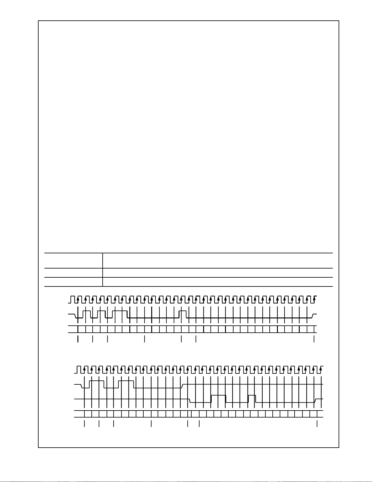
2.1.2 Serial Management Access Protocol
The serial control interface consists of two pins, Management Data Clock (MDC) and Management Data Input/Out-
and no minimum rate. The MDIO line is bi-directional and
may be shared by up to 32 devices. The MDIO frame format is shown in Table 1.
The MDIO pin requires a pull-up resistor (1.5 kΩ) which,
during IDLE and turnaround, will pull MDIO high. In order
to initialize the MDIO interface, the Station Management
Entity (SME) sends a sequence of 32 contiguous logic
ones on MDIO to provide the DP83843 with a sequence
that can be used to establish synchronization. This preamble may be generated either by driving MDIO high for 32
consecutive MDC clock cycles, or by simply allowing the
MDIO pull-up resistor to pull the MDIO pin high during
which time 32 MDC clock cycles are provided. In addition
32 MDC clock cycles should be used if an invalid start, op
code, or turnaround bit is detected.
The DP83843 waits until it has received this preamble
sequence before responding to any other transaction.
Once the DP83843 serial management port has initialized
no further preamble sequencing is required until after a
power-on/reset has occurred.
The Start code isindicated by a <01>pattern.This assures
the MDIO line transitions from the default idle line state.
Turnaround is an idle bit time inserted between the Register Address field andthe Data field. To avoid contention, no
device actively drives the MDIO signal during the first bit of
Turnaround during a read transaction. The addressed
DP83843 drives the MDIO with a zero for the second bit of
turnaround and follows thiswith the required data. Figure 2
shows the timing relationship between MDC and the MDIO
as driven/received by the Station Management Entity and
the DP83843 (PHY) for a typical register read access.
put (MDIO). MDC has a maximum clock rate of 2.5 MHz
Table 1. Typical MDIO Frame Format
MII Management
<idle><start><op code><device addr> <reg addr><turnaround><data><idle>
Serial Protocol
Read Operation <idle><01><10><AAAAA> <RRRRR><Z0><xxxx xxxx xxxx xxxx><idle>
Write Operation <idle><01><01><AAAAA> <RRRRR><10><xxxx xxxx xxxx xxxx><idle>
MDC
MDIO
(SME)
MDC
MDIO
(SME)
MDIO
(PHY)
00011110000000
Z
Idle Start
Opcode
(Write)
PHY Address
(PHYAD = 0Ch)
Register Address
(00h = BMCR)
Figure 1. Typical MDC/MDIO Write Operation
Z
Z
00011 110000000
Idle Start
Opcode
(Read)
PHY Address
(PHYAD = 0Ch)
Register Address
Figure 2. Typical MDC/MDIO Read Operation
(00h = BMCR)
ZZ
0 0 0 000 00000000
1000
TA
Z
Z
Z
0 0 011000100000000
TA
Register Data
Register Data
Z
Idle
Z
Z
Idle
13 www.national.com

2.0 Functional Description (Continued)
For write transactions, the Station Management Entity
writes data to an addressed DP83843 eliminating the
requirement for MDIO Turnaround. The Turnaround time is
filled by the management entity inserting <10> for these
two bits. Figure 1shows the timing relationship for a typical
MII register write access.
2.1.3 Preamble Suppression
The DP83843 supports a Preamble Suppression mode as
indicated by a one in bit 6 of the Basic Mode Status Register (BMSR, address 01h). If the Station Management Entity
(i.e. MAC or other management controller) determines that
all PHYs in the system support Preamble Suppression by
returning a one in this bit, then the Station Management
Entity need not generate preamble for each management
transaction.
The DP83843 requires a single initialization sequence of
32 bits of preamble following power-up/hardware reset.
This requirement is generallymet by the mandatory pull-up
resistor on MDIO in conjunction with a continuous MDC, or
the management access made to determine whether Preamble Suppression is supported.
While the DP83843 requires an initial preamble sequence
of 32 bits for management initialization, it does not require
a full 32 bit sequence between each subsequent transaction. A
transactions is required
2.1.4 PHY Address Sensing
The DP83843 can be set to respond to any of the possible
32 PHY addresses. Each DP83843 connected to a common serial MII must have a unique address. It should be
noted that while an address selection of all zeros <00000>
will result in PHY Isolate mode, this will not effect serial
management access.
The DP83843 provides five PHY address pins, the state of
which are latched into the PHYCTRL register (address
19h) at system power-up/reset. These pins are described
in Section 2.8. For further detail relating to the latch-in timing requirements of the PHY address pins, as well as the
other hardware configuration pins, refer to Section 3.10.
2.1.5 Nibble-wide MII Data Interface
Clause 22 of the IEEE 802.3u specification defines the
Media Independent Interface. This interface includes a
dedicated receive bus and a dedicated transmitbus. These
two data buses, along with various control and indicate signals, allow for the simultaneous exchange of data between
the DP83843and the upper layer agent(MAC or repeater).
The receive interface consists of a nibble wide data bus
RXD[3:0], a receive error signal RX_ER, a receive data
valid flag RX_DV, anda receive clock RX_CLK for synchronous transfer of the data. The receive clock can operate at
either 2.5 MHz to support 10 Mb/s operation modes or at
25 MHz to support 100 Mb/s operational modes.
The transmit interface consists of a nibble wide data bus
TXD[3:0], a transmit error flag TX_ER, a transmit enable
control signal TX_EN, and a transmit clock TX_CLK which
runs at either 2.5 MHz or 25 MHz.
Additionally, the MII includes the carrier sense signal CRS,
as well as a collision detect signal COL. The CRS signal
asserts to indicate the reception of data from the network
or as a function of transmit data in Half Duplex mode. The
COL signal asserts asan indication of a collisionwhich can
minimum of one idle bit between management
as specified in IEEE 802.3u.
occur during half-duplex operation when both a transmit
and receive operation occur simultaneously.
2.1.6 Collision Detect
For Half Duplex, a 10BASE-T or 100BASE-X collision is
detected when the receive and transmit channels are
active simultaneously. Collisions are reported by the COL
signal on the MII.
If the DP83843 is transmitting in 10 Mb/s modewhen a collision is detected, the collision is not reported until seven
bits have been received while in the collision state. This
prevents a collision being reported incorrectly due to noise
on the network. The COL signal remains set for the duration of the collision.
If a collision occurs during a receive operation, it is immediately reported by the COL signal.
When heartbeat is enabled (only applicable to 10 Mb/s
operation), approximately 1 µs after the transmission of
each packet,a Signal Quality Error (SQE) signal ofapproximately 10 bit times is generated (internally) to indicate
successful transmission. SQEis reported as a pulse on the
COL signal of the MII.
2.1.7 Carrier Sense
Carrier Sense (CRS) may be asserted due to receiveactivity, once valid data is detected via the Smart Squelch function during 10 Mb/s operation.
For 10 Mb/s Half Duplex operation, CRS is asserted during
either packet transmission or reception.
For 10 Mb/s Full Duplex operation, CRS is asserted only
due to receive activity.
CRS is deasserted following an end of packet.
In Repeater mode(pin 63/bit 9, register address19h), CRS
is only asserted due to receive activity.
2.1.8 MII Isolate Mode
A 100BASE-X PHY connected to the mechanical MII interface specified in IEEE 802.3u is required to have a default
value of one in bit 10 of the Basic Mode Control Register
(BMCR, address 00h). The DP83843 will set this bit to one
if the PHY Address is set to 00000 upon power-up/hardware reset. Otherwise, the DP83843 will set this bit to zero
upon power-up/hardware reset.
With bit 10 in the BMCR set to one, the DP83843 does not
respond to packet data present at TXD[3:0], TX_EN, and
TX_ER inputs and presents a high impedance on the
TX_CLK, RX_CLK, RX_DV, RX_ER, RXD[3:0], COL, and
CRS outputs. The DP83843 will continue to respond to all
serial management transactions over the MII.
While in Isolate mode, the TPTD+/− and FXTD/AUITD+/−
outputs are dependent on the current state of Auto-Negotiation. The DP83843 can Auto-Negotiate or parallel detect
to a specific technology depending on the receive signal at
the TPRD+/− inputs. A valid link can be established for
either TPRD or FXRD/AUI even when the DP83843 is in
Isolate mode.
It is recommended that the user have a basic understanding of clause 22 of the 802.3u standard.
14 www.national.com
2.0 Functional Description (Continued)
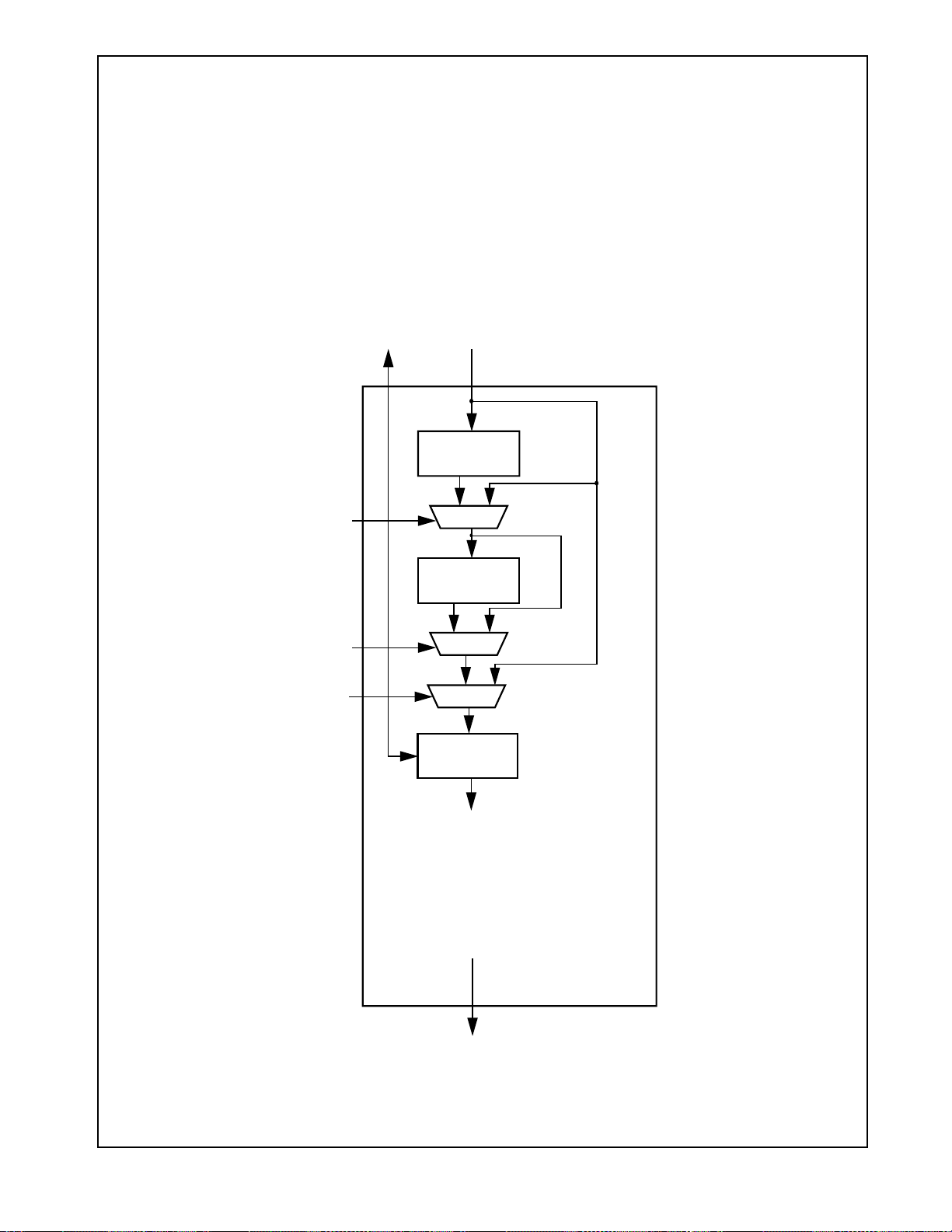
2.2 100BASE-TX TRANSMITTER
The 100BASE-TX transmitter consists of several functional
blocks which convert synchronous 4-bit nibbledata, as provided bythe MII, to a scrambled MLT-3 125 Mb/s serial data
stream. Because the 100BASE-TX TP-PMD is integrated,
the differential outputpins, TPTD+/−, can be directly routed
to the AC coupling magnetics.
The block diagram in Figure 3 provides an overview of
each functional block within the 100BASE-TX transmit section.
The Transmitter section consists of the following functional
blocks:
CODE-GROUP
ENCODER &
INJECTOR
— Code-group EncoderandInjection block(bypass option)
— Scrambler block (bypass option)
— NRZ to NRZI encoder block
— Binary to MLT-3 converter / Common Driver
The bypass option for the functional blocks within the
100BASE-X transmitter provides flexibility for applications
such as 100 Mb/s repeaters where data conversion is not
always required. The DP83843 implements the 100BASEX transmit state machine diagram as specified in the IEEE
802.3u Standard, Clause 24.
SCRAMBLER
PARALLEL
TO SERIAL
NRZ TO NRZI
ENCODER
Figure 1. 100BASE-TX Transmit Block Diagram
– Code-group Encoding and Injection
15 www.national.com

2.0 Functional Description (Continued)
The code-group encoder converts 4 bit (4B) nibble data
generated bythe MAC into5 bit (5B) code-groups for transmission. This conversion is required to allow control data to
be combined with packet data code-groups. Refer to Table
2 for 4B to 5B code-group mapping details.
The code-group encoder substitutes the first 8 bits of the
MAC preamble with a J/K code-group pair (11000 10001)
upon transmit. The code-group encoder continues to
replace subsequent 4B preamble and data nibbles with
corresponding 5B code-groups. At the end of the transmit
packet, upon the deassertion of Transmit Enable signal
from the MAC or Repeater, the code-group encoder injects
the T/R code-group pair (01101 00111) indicating the end
of frame.
After the T/R code-group pair, the code-group encoder
continuously injects IDLEs into the transmit data stream
until the next transmit packet is detected (reassertion of
Transmit Enable).
The DP83843 also incorporates a special injection function
which allowsfor fixed transmission of special repeating patterns for testing purposes. These special patterns are not
delimited with Start of Stream Delimiter (SSD) or End of
Stream Delimiter (ESD) code-groups and should not be
enabled during normal network connectivity.
These patterns, selectable via bits [8:7] of PCRS (address
16h), include:
8=0, 7=0: Normal operation (injection disabled)
8=0, 7=1: Transmit repeating FEFI pattern
8=1, 7=0: Transmit repeating 1.28 µs period squarewave
8=1, 7=1: Transmit repeating 160 ns period squarewave
Note that these patterns will be routed through thetransmit
scrambler and become scrambled (and therefore potentially less useful) unless the scrambler is bypassed via bit
12 of LBR (address 17h). It should be noted that if the
scrambler isbypassed by forcing the
quently resetting the device) the TPTD+/− outputs will
become disabled and the test pattern data will be routed to
the FXTD/AUITD+/− outputs. Additionally, the test patterns
will not be generated if the DP83843 is in symbol mode.
FXEN pin (and subse-
2.2.1 Scrambler
The scrambler is required to control the radiatedemissions
at the media connector and on the twisted pair cable (for
100BASE-TX applications). By scrambling the data, the
total energy launched onto the cable is randomly distributed over a wide frequency range. Without the scrambler,
energy levels at the PMD and on the cable could peak
beyond FCC limitations at frequencies related to repeating
5B sequences (i.e., continuous transmission of IDLEs).
The scrambler is configured as a closed loop linear feedback shift register (LFSR) with an 11-bit polynomial. The
output of the closed loop LFSR is combined with the NRZ
5B data from the code-group encoder via an X-OR logic
function. The result is a scrambled data stream with sufficient randomization to decrease radiated emissions at certain frequencies by as much as 20 dB. The DP83843 uses
the PHYID as determined by the PHYAD [4:0] pins to set a
unique seed value for thescrambler so thatthe total energy
produced by a multi-PHY application (i.e. repeater) distributes the energy out of phase across the spectrum and
helps to reduce overall electro-magnetic radiation.
The scrambler is automatically bypassed when the
DP83843 is placed in
tively, controlled by bit 12 of LBR (address 17h) via software.
2.2.2 NRZ to NRZI Encoder
After the transmit data stream has been scrambled and
serialized, the datamust be NRZI encodedin order to comply with the TP-PMD standard for 100BASE-TX transmission over Category-5 unshielded twisted pair cable. There
is no ability to bypass this block within the DP83843.
2.2.3 Binary to MLT-3 Convertor / Common Driver
The Binary to MLT-3 conversion is accomplished by converting the serial binary datastream output from the NRZI
encoder into two binary data streams with alternately
phased logic one events. These two binary streams are
then fed to the twisted pair output driver which converts
these streams to current sources and alternately drives
either side of the transmit transformer primary winding
resulting in a minimal current (20 mA max) MLT-3 signal.
Refer to Figure 4 .
FXEN mode via hardware or,alterna-
binary_in
binary_in
D
Q
Q
CP
Figure 1. Binary to MLT-3 conversion
binary_plus
binary_minus
differential MLT-3
binary_plus
COMMON
DRIVER
binary_minus
16 www.national.com
MLT-3

2.0 Functional Description (Continued)
Table 2. 4B5B Code-Group Encoding/Decoding
Name PCS 5B Code-group MII 4B Nibble Code
DATA CODES
0 11110 0000
1 01001 0001
2 10100 0010
3 10101 0011
4 01010 0100
5 01011 0101
6 01110 0110
7 01111 0111
8 10010 1000
9 10011 1001
A 10110 1010
B 10111 1011
C 11010 1100
D 11011 1101
E 11100 1110
F 11101 1111
IDLE AND CONTROL CODES
H 00100 Halt code-group - Error code
I 11111 Inter-Packet Idle - 0000 (
J 11000 First Start of Packet - 0101 (Note 1)
K 10001 Second Start of Packet - 0101 (Note 1)
T 01101 First End of Packet - 0000 (Note 1)
R 00111 Second End of Packet - 0000 (Note 1)
INVALID CODES
V 00000 0110 or 0101 (
Note 2)
V 00001 0110 or 0101 (Note 2)
V 00010 0110 or 0101 (Note 2)
V 00011 0110 or 0101 (Note 2)
V 00101 0110 or 0101 (Note 2)
V 00110 0110 or 0101 (Note 2)
V 01000 0110 or 0101 (Note 2)
V 01100 0110 or 0101 (Note 2)
V 10000 0110 or 0101 (Note 2)
V 11001 0110 or 0101 (Note 2)
Note 1: Control code-groups I, J, K, T and R in data fields will be mapped as invalid codes, together with RX_ER asserted.
Note 2: Normally, invalidcodes (V)are mappedto 6hon RXD[3:0]with RX_ERasserted. Ifthe CODE_ERRbit inthe PCS (bit 3, register address 16h)
is set, the invalid codes are mapped to 5h on RXD[3:0] with RX_ER asserted. Refer to Section 4.14 for further detail.
Note 1)
17 www.national.com

2.0 Functional Description (Continued)
The 100BASE-TX MLT-3 signal sourced by the TPTD+/−
common driver output pins is slow rate controlled. This
should be considered when selecting AC coupling magnetics to ensure TP-PMD compliant transition times (3 ns < Tr
< 5ns).
The 100BASE-TX transmit TP-PMD function within the
DP83843 is capable of sourcing only MLT-3 encoded data.
Binary output from the TPTD+/− outputs is not possible in
100 Mb/s mode.
2.2.4 TX_ER
Assertion of the TX_ERinput while the TX_EN inputis also
asserted will cause the DP83843 to substitute HALT codegroups for the 5B data present at TXD[3:0]. However, the
SSD (/J/K/) and ESD (/T/R/) will not be substituted with
Halt code-groups. As a result, the assertion of TX_ER
while TX_EN is asserted will result in a frame properly
encapsulated with the /J/K/ and /T/R/ delimiters which contains HALT code-groups in place of the data code-groups.
2.2.5 TXAR100
The transmit amplitude of the signal presented at the
TPTD+/− outputpins can be controlled byvarying the value
of resistance between TXAR100 and system GND. This
TXAR100 resistor sets up a reference current that determines the final output current at TPTD+/−.
For 100Ω Category-5 UTP cable implementations, the
TXAR100 resistor may be omitted as the DP83843 was
designed to source a nominal 2V pk-pk differential transmit
amplitude with this pin left floating. Setting the transmit
amplitude to 2V pk-pk differential (MLT-3) as measured
across the RJ45-8 transmit pins is critical for complying
with the IEEE/ANSI TP-PMD specification of 2.0V pk-pk
differential ±5%.
2.3 100BASE-TX RECEIVER
The 100BASE-TX receiver consists of several functional
blocks which convert the scrambled MLT-3 125 Mb/s serial
data stream to synchronous 4-bit nibble data that is provided to the MII. Because the 100BASE-TX TP-PMD is
integrated, the differential input pins, TPRD+/−, can be
directly routed to the AC coupling magnetics.
See Figure 5 for a block diagram of the 100BASE-TX
receive function. This provides an overview of each functional block within the 100BASE-TX receive section.
The Receive section consists of the following functional
blocks:
— Input and BLW Compensation
— Signal Detect
— Digital Adaptive Equalization
— MLT-3 to Binary Decoder
— Clock Recovery Module
— NRZI to NRZ Decoder
— Serial to Parallel
— DESCRAMBLER (bypass option)
— Code Group Alignment
— 4B/5B Decoder (bypass option)
— Link Integrity Monitor
— Bad SSD Detection
The bypass option for the functional blocks within the
100BASE-X receiver provides flexibility for applications
such as 100 Mb/s repeaters where data conversion is not
always required.
2.3.1 Input and Base Line Wander Compensation
Unlike the DP83223V TWISTER™, the DP83843 requires
no external attenuation circuitry at its receive inputs,
TPRD+/−. The DP83843accepts TP-PMD compliant waveforms directly, requiring only a 100Ω termination plus a
simple 1:1 transformer. The DP83843 also requires external capacitance to V
ure 23). This establishes a solid common mode voltage
that is needed since the TPRD pins are used in both 10
Mb/s and 100 Mb/s modes.
The DP83843 is completely ANSI TP-PMD compliant
because it compensates for baseline wander. The BLW
compensation block can successfully recover the TP-PMD
defined “killer” pattern and pass it to the digital adaptive
equalization block.
Baseline wander cangenerally be defined as thechange in
the average DC content, over time, of an AC coupled digital
transmission over a given transmission medium. (i.e. copper wire).
Baseline wander results from the interaction between the
low frequency components of a bit stream being transmitted and the frequency response of the AC coupling component(s) within thetransmission system. If the low frequency
content of the digital bit stream goes below the low frequency pole of the AC coupling transformers then the
droop characteristics of the transformers will dominate
resulting in potentially serious baseline wander.
It is interesting to note that the probability of a baseline wander event serious enough to corrupt data is very low. In fact,
it is reasonable to virtually bound the occurrence of a baseline wander event serious enough to cause bit errors to a
legal but premeditated, artificially constructed bit sequence
loaded into the original MAC frame. Several studies have
been conducted to evaluate the probability of various baseline wander events for FDDI transmission over copper. Contact the X3.263 ANSI group for further information.
2.3.2 Signal Detect
The signal detect function of the DP83843 is incorporated
to meet the specificationsmandated by the ANSI FDDI TPPMD Standard as well as the IEEE 802.3 100BASE-TX
Standard for both voltage thresholds and timing parameters.
Note that the reception of Normal 10BASE-T link pulses
and fast link pulses per IEEE 802.3u Auto-Negotiation by
the 100BASE-X receiver do not cause the DP83843 to
assert signal detect.
While signal detect is normally generated and processed
entirely within the DP83843, it can be observed directly on
the CRS pin (pin 22) while the DP83843 is configured for
Symbol mode.Refer to Section3.4 for further detailregarding Symbol mode operation.
2.3.3 Digital Adaptive Equalization
When transmitting data at high speeds over copper twisted
pair cable, frequency dependent attenuation becomes a
concern. In high speed twisted pair signalling, the frequency content of the transmitted signal can vary greatly
during normal operation based primarily on the randomness of the scrambled data stream. This variation in signal
at the VCM_CAP pin (refer to Fig-
CC
18 www.national.com

2.0 Functional Description (Continued)
CARRIER
INTEGRITY
MONITOR
LINK INTEG-
RITY MONITOR
RX_DATA
VALID SSD
DETECT
RX_CLK RXD[3:0] / RX_ER
BP_RX
BP_4B5B
BP_SCR
MUX
MUX
4B/5B
DECODER
CODE GROUP
ALIGNMENT
MUX
DESCRAMBLER
SD
CLOCK
CLOCK
RECOVERY
MODULE
DAT A
SERIAL TO
PARALLEL
NRZI TO NRZ
DECODER
MLT-3 TO
BINARY
DECODER
DIGITAL
ADAPTIVE
EQUALIZATION
INPUT
&BLW
COMPEN-
SATION
SIGNAL
DETECT
TPRD +/−
Figure 1. Receive Block Diagram
19 www.national.com
2.0 Functional Description (Continued)
t
attenuation caused by frequency variations must be compensated for to ensure the integrity of the transmission.
In order to ensure quality transmission when employing
MLT-3 encoding, the compensation must be able to adapt
to various cable lengths and cable types depending on the
installed environment. The selection of long cable lengths
for a given implementation, requires significant compensation which will over-compensate for shorter, less attenuating lengths. Conversely, the selection of short or
intermediate cable lengths requiring less compensation will
cause serious under-compensation for longer length
cables. Therefore, the compensation or equalization must
be adaptive to ensure proper conditioning of the received
signal independent of the cable length.
The DP83843 utilizes an extremely robust equalization
scheme referred to herein as ‘Digital Adaptive Equalization.’ Existing designs use an adaptive equalization scheme
that determines the approximate cable length by monitoring signal attenuation at certain frequencies. This attenuation value was compared to the internal receive input
reference voltage. This comparison would indicate that
amount of equalization to use. Although this scheme is
used successfully on the DP83223V TWISTER, it is sensitive totransformer mismatch, resistor variation and process
induced offset. The DP83223V also required an external
attenuation network to help match the incoming signal
amplitude to the internal reference.
Digital Adaptive Equalization is based on an advanced digitally controlled signal tracking technique. This method
uses peak tracking with digital over-sampling and digitally
controlled feedback loops to regenerate the receive signal.
This technique does not depend on input amplitude variations to set the equalization factor. As a result it maintains
constant jitter performance for any cable length up to 150
meters of CAT-5. Digital Adaptive Equalization allows for
very high tolerance to signal amplitude variations.
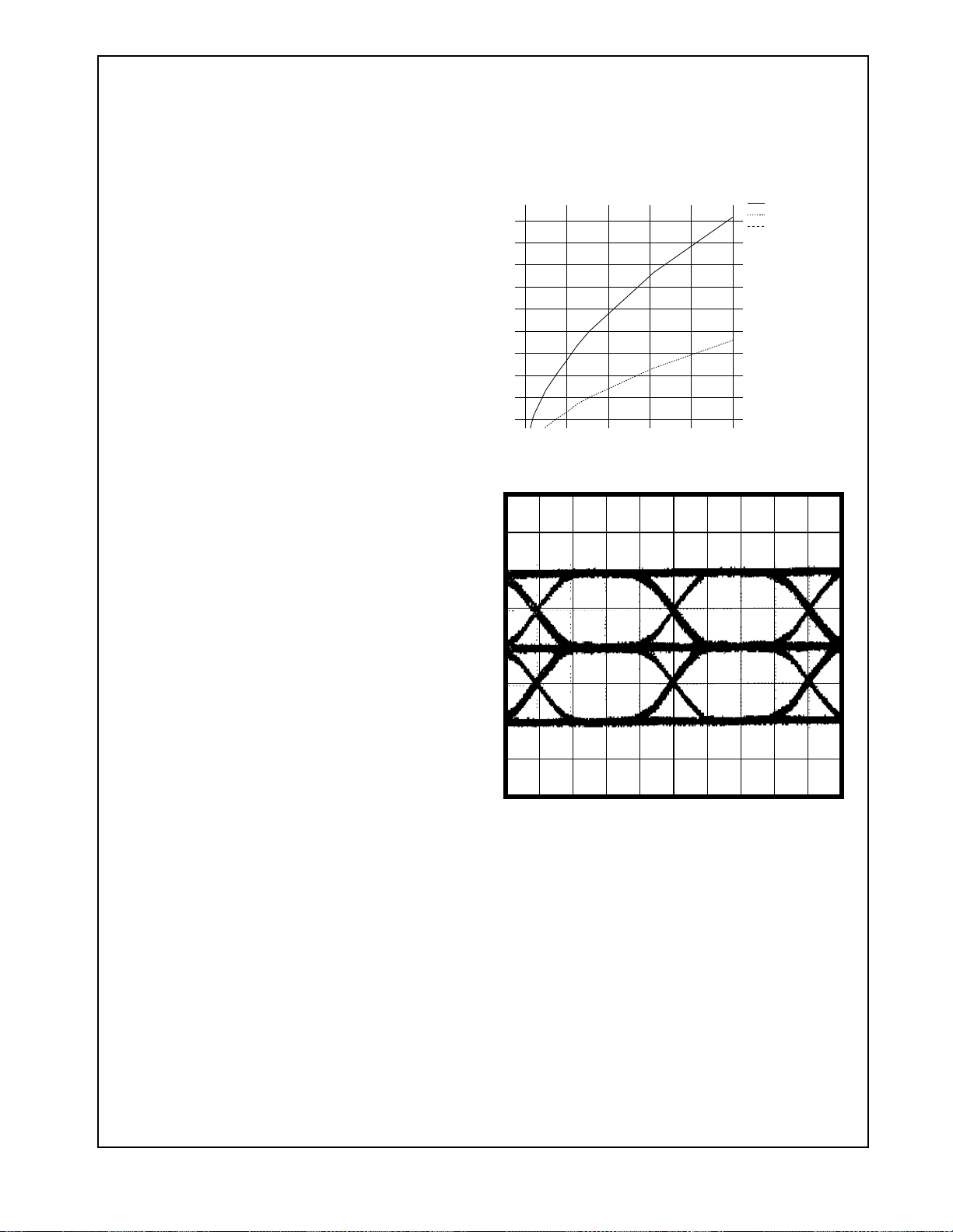
The curves given in Figure 6illustrate attenuation at certain
frequencies forgiven cablelengths. This isderived from the
worst case frequency vs. attenuation figures as specified in
the EIA/TIA BulletinTSB-36. These curves indicate the significant variations in signal attenuation that must be compensated for by the receive adaptive equalization circuit.
Figure 7 represents a scrambled IDLE transmitted over
zero meters of cable as measured at the AII (Active Input
Interface) of the receiver. Figure 8 and Figure 9 represent
the signal degradation over 50 and 100 Meters of CAT-5
cable respectively, also measured at the AII. These plots
show the extreme degradation of signal integrity and indicate the requirement for a robust adaptive equalizer.
The DP83843 provides the added flexibility of controlling
the type of receive equalization required for a given implementation. This is done through TW_EQSEL (bits [13:12]
of the PHYCTRLregister, address 19h).While digital adaptive equalization is the preferred method of cable compensation for 100BASE-TX, the ability to switch the equalizer
completely off or to a fixed maximum is provided. This feature is intended as a test mode only and, if enabled, will
inhibit normal performance of the DP83843.
2.3.4 MLT-3 to NRZI Decoder
The DP83843 decodes theMLT-3 information from the Digital Adaptive Equalizer block to binary NRZI data. The relationship of binary to MLT-3 data is shown in Figure 4.
enuation (dB)
22.00
20.00
18.00
16.00
14.00
12.00
10.00
8.00
6.00
4.00
100M
50M
0M
Figure 1. EIA/TIA Attenuation vs Frequency for 0, 50,
100 meters of CAT-5 cable
2ns/div
Figure 2. MLT-3 SignalMeasured atAII after0 metersof
2.3.5 Clock Recovery Module
The Clock Recovery Module (CRM) accepts 125 Mb/s
NRZI datafrom the MLT-3 to NRZI decoder. TheCRM locks
onto the 125 Mb/sdata stream and extracts a 125 MHz reference clock. The extracted and synchronized clock and
data are used as required by the synchronous receive
operations as generally depicted in Figure 5.
The CRM is implemented using an advanced digital Phase
Locked Loop (PLL) architecture that replaces sensitive
analog circuits. Using digital PLL circuitry allows the
DP83843 to be manufactured and specified to tighter tolerances.
For further information relating to the 100BASE-X clock
recovery module, refer to Section 4.3.
CAT-5 cable
20 www.national.com

2.0 Functional Description (Continued)
2ns/div
Figure 1. MLT-3 Signal Measured at AII after 50 meters
of CAT-5 cable
2ns/div
Figure 2. MLT-3 Signal Measured at AII after 100 meters
of CAT-5 cable
2.3.6 NRZI to NRZ
In a typical application, the NRZI to NRZ decoder is
required in order to present NRZ formatted data to the
descrambler (or to the code-group alignment block, if the
descrambler is bypassed, or directly to the PCS, if the
receiver is bypassed).
The receive data stream is in NRZI format, therefore, the data
must be decoded to NRZ before further processing.
2.3.7 Serial to Parallel
The 100BASE-X receiver includes a Serial to Parallel converter which supplies 5 bit wide data symbols to the
Descrambler. Converting to parallel helps to decrease
latency through the device, as well as performing the
required function for ultimately providing data to the nibblewide interface of the MII.
2.3.8 Descrambler
A 5-bit parallel (code-group wide) descrambler is used to
descramble the receive NRZ data. To reverse the data
scrambling process, the descrambler has to generate an
identical data scrambling sequence (N) in order to recover
the original unscrambled data (UD) from the scrambled
data (SD) as represented in the equations:
SD UD N⊕()=
UD SD N⊕()=
Synchronization of the descrambler to the original scrambling sequence (N) is achieved based on the knowledge
that the incoming scrambled data stream consists of
scrambled IDLE data. After the descrambler has recognized 12 consecutive IDLE code-groups, where an IDLE
code-group in 5B NRZ is equal to five consecutive ones
(11111), it will synchronize to the receive data stream and
generate unscrambled data in the form of unaligned 5B
code-groups.
In order to maintain synchronization, the descrambler must
continuously monitor the validity of the unscrambled data
that it generates. To ensure this, a line state monitor and a
hold timer are used to constantly monitor the synchronization status. Upon synchronization of the descrambler the
hold timer starts a 722 µs countdown. Upon detection of
sufficient IDLE code-groups within the 722 µs period, the
hold timer will reset and begin anew countdown. Thismonitoring operation will continue indefinitely given a properly
operating network connection with good signal integrity. If
the line state monitor does not recognize sufficient
unscrambled IDLE code-groups within the 722 µs period,
the entire descrambler will be forced out of the current state
of synchronization andreset in order to re-acquire synchronization.
The value of the time-out for this timer may be modified
from 722 sto 2 ms by setting bit 12 of the PCSR (address
16h) to one.The 2 ms option allows applications with Maximum Transmission Units (packet sizes) larger than IEEE
802.3 specifications to maintain descrambler synchronization (i.e. switch or router applications).
Additionally, this timer may be disabled entirely by setting
bit 11 of the PCSR (address 16h) to one. The disabling of
the time-out timer is not recommended as this will eventually result in a lackof synchronization between the transmit
scrambler and the receive descrambler which will corrupt
data. The descrambler time-out counter may be reset bybit
13 of the PCSR.
2.3.9 Code-group Alignment
The code-group alignment module operates on unaligned
5-bit data from the descrambler (or, if the descrambler is
bypassed, directly from the NRZI/NRZ decoder) and converts it into 5B code-group data (5 bits). Code-group alignment occurs after the J/K code-group pair is detected.
Once the J/K code-group pair (11000 10001) is detected,
subsequent data is aligned on a fixed boundary.
2.3.10 4B/5B Decoder
The code-group decoder functions as a look up table that
translates incoming 5B code-groups into 4B nibbles. The
code-group decoder first detects the J/K code-group pair
preceded by IDLE code-groups and replaces the J/K with
21 www.national.com

2.0 Functional Description (Continued)
the MAC preamble. Specifically, the J/K 10-bit code-group
pair is replaced by the nibble pair (0101 0101). All subsequent 5B code-groups are converted to the corresponding
4B nibbles for the duration of the entire packet. This conversion ceases upon the detection of the T/R code-group
pair denoting theEnd of Stream Delimiter(ESD) or with the
reception of a minimum of two IDLE code-groups.
2.3.11 100BASE-X Link Integrity Monitor
The 100BASE-X Link Integrity Monitor function (LIM)
allows the receiver to ensure that reliable data is being
received. Without reliable data reception, the LIM will halt
both transmit and receive operations until such time that a
valid link is detected (i.e. good link).
If Auto-Negotiation is not enabled, then a valid link will be
indicated once SD+/− is asserted continuously for 500 µs.
If Auto-Negotiation is enabled, then Auto-Negotiation will
further qualify a valid link as follows:
— The descrambler must receive a minimum of 12 IDLE
code groups for proper link initialization.
— The Auto-Negotiation must determine that the
100BASE-X function should be enabled.
A valid link for a non-Auto-Negotiating application is indicated by either the Link LED output or by reading bit 2 of
the Basic Mode Status Register BMSR (address 01h). For
a truly qualified valid link indication as a result of AutoNegotiation, bit 2 of the BMSR register (address 01h) must
be read.
2.3.12 Bad SSD Detection
A Bad Start ofStream Delimiter (Bad SSD)is any transition
from consecutive idle code-groups to non-idle code-groups
which is not prefixed by the code-group pair /J/K.
If this condition is detected, the DP83843 will assert
RX_ER and present RXD[3:0] = 1110 to the MII for the
cycles that correspond to received 5B code-groups. In
order to exit this state the PHYTER must receive at least
two IDLE code groups and the PHYTER cannot receive a
single IDLE code group at any time. In addition, the False
Carrier Event Counter (address 14h) will be incremented
by one. Once the PHYTER exits this state, RX_ER and
CRS become de-asserted.
When bit 11 of the LBR register is one (BP_RX), RXD[3:0]
and RX_ER/RXD[4] are not modified.
2.3.13 Carrier Integrity Monitor
The Carrier Integrity Monitor function (CIM) protects the
repeater from transient conditions that would otherwise
cause spurious transmission due to a faulty link. This function is required for repeater applications and is not specified for node applications.
The REPEATER pin (pin63) determines the defaultstate of
bit 5 of the PCS register (Carrier Integrity Monitor Disable,
address 16h) to automatically enable or disable the CIM
function as required for IEEE 802.3 compliant applications.
After power-up/reset, software may enable or disable this
function independent of Repeater or Node mode.
If the CIM determines that the link is unstable, the
DP83843 will not propagate the received data or control
signaling to the MII and will ignore data transmitted via the
MII. The DP83843 will continue to monitor the receive
stream for valid carrier events.
Detection of an unstable link condition will cause bit 4 of
the PCS register (address 16h) to be set to one. This bit is
cleared to zero upon a read operation once a stable link
condition is detected by the CIM. Upon detection of a stable link, the DP83843 will resume normal operations.
The Disconnect Counter (address 13h) increments each
time the CIM determines that the link is unstable.
2.4 10BASE-T TRANSCEIVER MODULE
The 10BASE-T Transceiver Module is IEEE 802.3 compliant. It includes the receiver, transmitter, collision, heartbeat, loopback, jabber, and link integrity functions, as
defined in the standard. An external filter is not required on
the 10BASE-T interface since this is integrated inside the
DP83843. Due to the complexity and scope of the
10BASE-T Transceiver block and various sub-blocks, this
section focuses on the general system level operation.
2.4.1 Operational Modes
The DP83843 has 2 basic 10BASE-T operational modes:
Half Duplex mode
Full Duplex mode
Half Duplex Mode
In Half Duplex mode the DP83843 functions as a standard
IEEE 802.3 10BASE-T transceiver supporting the
CSMA/CD protocol.
Full Duplex Mode
In Full Duplex mode the DP83843 is capable of simultaneously transmitting and receiving without asserting the
collision signal. The DP83843's 10 Mb/s ENDEC is
designed to encode and decode simultaneously.
2.4.2 Oscillator Module Operation
A 25 MHzcrystalor can-oscillator with thefollowing specifications is recommended for driving the X1 input.
1. CMOS output with a 50ppm frequency tolerance.
2. 35-65% duty cycle (max).
3. Two TTL load output drive.
Additional output drive may be necessary if the oscillator
must also drive other components. When using a clock
oscillator it is still recommended that the designer connect
the oscillator output to the X1 pin and leave X2 floating.
2.4.3 Smart Squelch
The smart squelch is responsible for determining when
valid data is present on the differential receive inputs
(TPRD+/−). The DP83843 implements an intelligent
receive squelchto ensure that impulsenoise on the receive
inputs will not be mistaken for a valid signal. Smart squelch
operation is independent of the 10BASE-T operational
mode.
The squelch circuitry employs a combination of amplitude
and timing measurements (as specified in the IEEE 802.3
10BASE-T standard) to determine the validity of data on
the twisted pair inputs (refer to Figure 10).
The signal at the start of packet is checked by the smart
squelch and any pulses not exceeding the squelch level
(either positive or negative, depending upon polarity) will
be rejected. Once this first squelch level is overcome correctly, the opposite squelch level must then be exceeded
within 150 ns. Finally the signal must exceed the original
squelch level within a further 150 ns to ensure that the
22 www.national.com

2.0 Functional Description (Continued)
Twisted Pair Squelch Operation
<150ns <150ns >150ns
Vsq +
Vsq +
reduced
Vsq -
reduced
Vsq -
start of packet end of packet
Figure 1. 10BASE-T Twisted Pair Smart Squelch Operation
input waveform will not be rejected. The checking procedure results in the loss of typically three preamble bits at
the beginning of each packet.
Only after all these conditions have been satisfied will a
control signal be generated to indicate to the remainder of
the circuitry that valid data is present. At this time, the
smart squelch circuitry is reset.
Valid data is considered to be present until squelch level
has not been generated for a time longer than 150ns, indicating the End of Packet. Once good data has been
detected the squelch levels are reduced to minimize the
effect of noise causing premature End of Packet detection.
The receive squelch threshold level can be lowered for use
in longer cable applications. This is achieved by setting the
LS_SEL bit in the 10BTSCR (bit 6, register 18h). Collision
Detection
For Half Duplex, a10BASE-T collision is detectedwhen the
receive and transmit channels are active simultaneously.
Collisions are reported by the COL signal on the MII.
If the ENDEC is transmitting when a collision is detected,
the collision is not reported until seven bits have been
received while in the collision state. This prevents a collision beingreportedincorrectly due to noiseon the network.
The COL signalremains set forthe duration of thecollision.
If the ENDEC is receiving when a collision is detected it is
reported immediately (through the COL).
When heartbeat is enabled, approximately 1 µs after the
transmission of each packet, a Signal Quality Error (SQE)
signal of approximately 10 bit times is generated (internally) to indicate successful transmission. SQE is reported
as a pulse on the COL signal of the MII.
2.4.4 Carrier Sense
Carrier Sense (CRS) may be asserted due to receiveactivity once valid data is detected via the smart squelch function.
For 10 Mb/s Half Duplex operation, CRS is asserted during
either packet transmission or reception.
For 10 Mb/s Full Duplex operation, CRS is asserted only
due to receive activity.
CRS is deasserted following an end of packet.
In Repeater mode, CRS is only asserted due to receive
activity.
2.4.5 Normal Link Pulse Detection/Generation
The link pulse generator produces pulses as defined in the
IEEE 802.3 10BASE-T standard. Each link pulse is nominally 100 ns in duration and is transmitted every 16 ms ± 8
ms, in the absence of transmit data.
Link pulse is used to check the integrity of the connection
with the remote end. If valid link pulses are not received,
the link detector disables the 10BASE-T twisted pair transmitter, receiver and collision detection functions.
When the link integrity function is disabled, the 10BASE-T
transceiver will operate regardless of the presence of link
pulses.
2.4.6 Jabber Function
The jabber function monitors the DP83843's output and
disables the transmitter if it attempts to transmit a packet of
longer than legal size. A jabber timer monitorsthe transmitter and disables the transmission if the transmitter is active
for approximately 20-30 ms.
Once disabled by the Jabber function, the transmitter stays
disabled for the entire time that the ENDEC module's internal transmit enable is asserted. This signal has to be deasserted for approximately 400-600 ms (the “unjab” time)
before the Jabber function re-enables the transmit outputs.
The Jabberfunction is only meaningfulin 10BASE-T mode.
2.4.7 Status Information
10BASE-T Status Information is available on the LED output pins of the DP83843. Transmit activity, receive activity,
link status, link polarity and collision activity information is
output to the five LED output pins (LED_RX, LED_TX,
LED_LINK, LED_FDPOL, and LED_COL). Additionally, the
active high SPEED10 output will assert to indicate 10 Mb/s
operation.
If required, the LED outputs can be used to provide digital
status information to external circuitry.
The link LED output indicates good link status for both 10
and 100 Mb/s modes. In Half Duplex 10BASE-T mode,
LED_LINK indicates link status.
The link integrity function can be disabled. When disabled,
the transceiver will operate regardless of the presence of
link pulses andthe link LED will stay asserted continuously.
2.4.8 Automatic Link Polarity Detection
The DP83843's 10BASE-T transceiver module incorporates an automatic link polarity detection circuit. When
seven consecutive link pulses or three consecutive receive
23 www.national.com

2.0 Functional Description (Continued)
packets with inverted End-of-Packet pulses are received,
bad polarity is reported.
A polarity reversalcan be caused by a wiring error at either
end of the cable, usually at the Main Distribution Frame
(MDF) or patch panel in the wiring closet.
The bad polarity condition is latched and the LED_ FDPOL
output is asserted. The DP83843's 10BASE-T transceiver
module corrects for this error internally and will continue to
decode received data correctly. This eliminates the need to
correct the wiring error immediately.
2.4.9 10BASE-T Internal Loopback
When the 10MB_ENDEC_LB bit in the LBR (bit 4, register
address 17h) is set, 10BASE-T transmit data is looped
back in the ENDEC to the receive channel. The transmit
drivers and receive input circuitry are disabled in transceiver loopback mode, isolating the transceiver from the
network.
Loopback is used for diagnostic testing of the data path
through the transceiver without transmitting on the network
or being interrupted by receive traffic. This loopback function causes thedata to loopback just prior to the 10BASE-T
output driver bufferssuch that the entire transceiver path is
tested.
2.4.10 Transmit and Receive Filtering
External 10BASE-T filters are not required when using the
DP83843 as the required signal conditioning is integrated.
Only isolation/step-up transformers and impedance matching resistors are required for the 10BASE-T transmit and
receive interface. The internal transmit filtering ensures
that all the harmonics in the transmit signal are attenuated
by at least 30 dB.
2.4.11 Encoder/Decoder (ENDEC) Module
The ENDEC module consists of essentially four functions:
The oscillator generates the 10 MHz transmit clock signal
for system timing from an external 25 MHz oscillator.
The Manchester encoder accepts NRZ data from the con-
troller or repeater, encodes the data to Manchester, and
transmits it differentially to the transceiver, through the differential transmit driver.
The Manchester decoder receives Manchester data from
the transceiver, converts it to NRZ data and recovers clock
pulses for synchronous data transfer to the controller or
repeater.
The collision monitor indicates to the controller the presence of a valid 10 Mb/s collision signal.
2.4.12 Manchester Encoder
The encoder begins operation when the Transmit Enable
input (TX_EN) goes high and converts the NRZ data to
pre-emphasized Manchester data for the transceiver. For
the duration of TX_EN remaining high, the Transmit Data
(TPTD+/−) is encoded for the transmit-driver pair
(TPTD+/−). TXD must be valid on the rising edge of Transmit Clock (TX_CLK). Transmission ends when TX_EN
deasserts. The last transition is always positive; itoccurs at
the center of the bit cell if the last bit is a one, or at the end
of the bit cell if the last bit is a zero.
2.4.13 Manchester Decoder
The decoder consists of adifferential receiver and a PLL to
separate a Manchester encoded data stream into internal
clock signals and data. The differential input must be externally terminated with either a differential 100ohm termination network to accommodate UTP cable.
The decoderdetects the end ofa frame whenno more midbit transitions are detected. Within one and a half bit times
after the last bit, carrier sense is de-asserted. Receive
clock stays active for five more bit times after CRS goes
low, to guarantee the receive timings of the controller or
repeater.
2.5 100 BASE-FX
The DP83843 is fully capable of supporting 100BASE-FX
applications. 100BASE-FX is similar to 100BASE-TX with
the exceptionsbeing the PMD sublayer,lack of datascrambling, and signalingmedium and connectors. Chapter 26 of
the IEEE 802.3u specification defines the interface to this
PMD sublayer.
The DP83843 can be configured for 100BASE-FX operation either through hardware or software. Configuration
through hardware is accomplished byforcing the
(pin 21) to a logic low level prior to power-up/reset. Configuration through software is accomplished bysetting bits 9:7
of the LBRregister to <011>, enabling FEFI (bit 14 of register PCSR(16h)), bypassing the scrambler (bit 12 of register
LBR(17h)) and disabling Auto-Negotiation. In addition, setting the FX_EN bit of the PHYCTRL register (bit 5, address
19h) accomplishes the same function as forcing the
pin (pin 21) to a logic low. In 100BASE-FX mode, the FX
interface is enabled along with the Far End Fault Indication
(FEFI) and Bypass Scrambler functions. Auto-Negotiation
must be disabled in order for 100BASE-FX operation to
work properly.
The diagram inFigure 11 is a block diagram representation
of the FX interface and the alternative data paths for transmit, receive and signal detect.
FXEN pin
FXEN
24 www.national.com

2.0 Functional Description (Continued)
NORMAL TX DATA
W/ SCRAMBLER BYPASSED
NRZ TO NRZI
ENCODER
BINARY
TO ML T-3 /
COMMON
DRIVER
TPTD+/−
PECL
DRIVER
FXTD
NORMAL RX DATA TO
DESCRAMBLER BYPASS
CLOCK
RECOVERY
MODULE
INPUT &BLW COMP
FULL ADAPT. EQUALIZ.
MLT-3 TO BINARY DEC.
PECL
INPUTS
TPRD+/−
NORMAL
SIGNAL DETECT
FXSDFXRD
SIGNAL
DETECT
Figure 1. 100Base-FX Block Diagram
2.5.1 FX Interface
When the FX interface is enabled the internal 100BASE-TX
transceiver is disabled. As defined by the 802.3u specification, PMD_SIGNAL_indicate (signal detect function),
PMD_UNITDATA.indicate (receive function), and
PMD_UNIT_DATA.request (transmit function) are supported by the FXSD+/−, FXRD+/−, and FXTD+/− pins
respectively.
Transmit
The DP83843 transmits NRZI data on the FXTD+/− pins.
This data is transmitted at PECL signal levels. 100BASEFX requires no scrambling/de-scrambling, so thescrambler
is bypassed in the transmit path. All other PMA and PCS
functions remain unaffected.
Receive
The DP83843 receives NRZI data on the FXRD+/− pins.
This data is accepted at PECL signal levels. 100BASE-FX
requires no scrambling/de-scrambling, so the de-scrambler
is bypassed in the receive path. All other PMA and PCS
functions remain unaffected.
Signal Detect
The DP83843 receives signal detect information on the
FXSD+/− pins. This data is accepted at PECL signal levels.
Signal detect indicates that a signal with the proper amplitude is present at the PMD sublayer.
2.5.2 Far End Fault Indication
Auto-Negotiation provides a mechanism for transferring
information from theLocal Station to the Link Partner that a
remote fault has occurred for 100BASE-TX. As Auto-Nego-
tiation is not currently specified for operation over fiber, the
Far End Fault Indication function (FEFI) provides some
degree of communication between link partners in support
of 100BASE-FX operation.
A remote fault is an error in the link that one station can
detect while the other cannot. An example of this is a disconnected fiber at a station’s transmitter. This station will
be receiving valid data and detect that the link is good via
the Link Integrity Monitor, but will not be able to detect that
its transmission is not propagating to the other station.
A 100BASE-FX station that detects such a remote fault
(through the deassertion of signal detect) may modify its
transmitted IDLE stream from all ones to a group of 84
ones followed by a single zero (i.e. 16 IDLE code groups
followed by a single Data 0 code group). This is referred to
as the FEFI IDLE pattern. Transmission of the FEFI IDLE
pattern will continue until FXSD+/− is re-asserted.
If three or more FEFI IDLE patterns are detected by the
DP83843, then bit 4 of the Basic Mode Status register
(address 01h) is set to one until read by management. It is
also set in bit 7 of the PHY Status register (address 10h).
The first FEFIIDLE pattern may containmore than 84 ones
as the pattern may have started during a normal IDLE
transmission which is actually quite likely. However, since
FEFI is a repeating pattern, this will not cause a problem
with the FEFI function. It should be noted receipt of the
FEFI IDLE pattern will not cause CRS to assert.
To enableFiber mode without FEFI, set bits 9:7 of the LBR
register to <011>, disable FEFI (bit 14 of register
PCSR(16h)), bypass the scrambler (bit 12 of register
25 www.national.com

2.0 Functional Description (Continued)
26 www.national.com
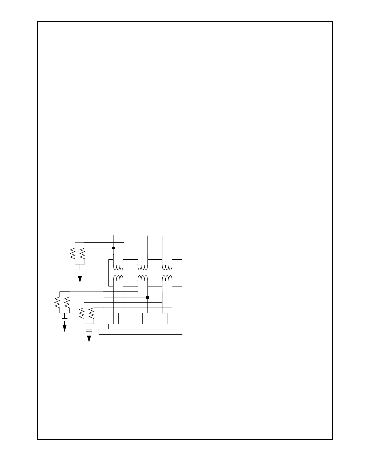
2.0 Functional Description (Continued)
The Manchester encoder accepts NRZ data from the MII,
encodes the data to Manchester and sends it to the driver.
The driver transmits the data differentially to the transceiver.
2.6.2 AUI/TP Autoswitch
The DP83843 has an autoswitching feature that allows
switching between the AUI and TP operation. The AUI/TPI
autoswitch feature (AUTOSW_EN) is enabled by bit 9 of
the 10BASE-T Control and Status Register (10BTSCR). If
AUTOSW_EN is asserted (default is de-asserted) and the
DP83843 is in 10 Mb/s mode it automatically activates the
TPI interface (10 Mb/s data is transmitted and received at
the TPTD+/− and TPRD+/− pins respectively). If there is an
absence of link pulses, the transceiver will switch to AUI
mode. Similarly, when the transceiver starts detecting link
pulses it will switch to TP mode. The switching from one
mode to the next is only done after the current packet has
been transmitted or received. If the twisted pair output is
jabbering and gets into link fail state, then the switch to AUI
mode is only doneafter the jabbering is done, including the
time it takes to unjab (unjab time).
2.6.3 Ethernet Cable Configuration / THIN Output
The DP83843 offers the choice of Thick Ethernet
(10BASE5) and Thin Ethernet (10BASE-2). The type of
cabling used is controlled through bit 3 of the 10BTSCR
register (address 18h). TheDP83843 also provides a THIN
output signal whichcan be used todisable/enable an external DC-DC converter which is required for 10BASE-2 applications to provide electrical isolation. This enables a
10BASE-2 and10BASE-5 common interface application.
AUITD
AUIRD
AUICD
39Ω
.01uf
200Ω
200Ω
100uH
39Ω
39Ω
39Ω
.01uf
15 Pin D AUI Connector
Figure 1. AUI Typical Setup
27 www.national.com

3.0 Configuration
This section includes information on the various configuration options available with the DP83843. The configuration
options described herein include:
— Auto-Negotiation
— PHY Address and LEDs
— Half Duplex vs Full Duplex
— 100M Symbol mode
— 100BASE-FX mode
— 10M serial MII mode
— 10M AUI Mode
— Repeater vs. Node
— Isolate mode
— Loopback mode
3.1 Auto-Negotiation
The Auto-Negotiation function provides a mechanism for
exchanging configuration information between two ends of
a link segment and automatically selecting the highest performance mode of operation supported by both devices.
Fast Link Pulse (FLP) Bursts provide the signaling used to
communicate Auto-Negotiation abilities between two
devices at each end of a link segment. For further detail
regarding Auto-Negotiation, refer to clause 28 of the IEEE
802.3u specification. The DP83843 supports four different
Ethernet protocols (10 Mb/s Half Duplex, 10 Mb/s Full
Duplex, 100 Mb/s Half Duplex, and 100 Mb/s Full Duplex),
so the inclusion of Auto-Negotiation ensures that the highest performance protocol will be selected based on the
ability of the Link Partner. The Auto-Negotiation function
within the DP83843 can be controlled either by internal
register access or by use of the AN1 and AN0 (pins 3 & 4).
3.1.1 Auto-Negotiation Pin Control
The state of AN0 and AN1 determines whether the
DP83843 is forced into a specific mode or Auto-Negotiation
will advertise a specific ability (or set of abilities) as given in
Table 3. Pins AN0 and AN1 are implemented as three-level
control pins which are configured by connecting them to
V
, GND, or by leaving them unconnected (refer to
CC
Figure 15). These pins allow configuration options to be
selected without requiring internal register access.
It should be noted that dueto the internal resistor networks
depicted in Figure 15, the AN0 or AN1 should be connected directly to either VCCor GND, depending on the
requirements. Thesepins should never be resistively tied to
V
or GND as this will interfere with the internal pull-up
CC
and pull-down resistors resulting in improper Auto-Negotiation behavior.
The state of AN0 and AN1, upon power-up/reset, determines the state of bit 9 in the PHYSTS register (address
10h) as well as bits [8:5] of the ANAR register (address
04h).
Upon power-up/reset the DP83843 uses default register
values, which enables Auto-Negotiation and advertises the
full set of abilities (10 Mb/s Half Duplex, 10 Mb/s Full
Duplex, 100 Mb/s Half Duplex, and 100 Mb/s Full Duplex)
unless subsequent software accesses modify the mode.
The status of Auto-Negotiation as a function of hardware
configuration via the AN0 and AN1 pins is reflected in bit 9
of the PHYSTS register (address 10h).
The Auto-Negotiation function selected at power-up or
reset can be changed at any time by writing to the Basic
Mode Control Register (BMCR) at address 00h.
3.1.2 Auto-Negotiation Register Control
When Auto-Negotiation is enabled, the DP83843 transmits
the abilities programmed into the Auto-Negotiation Advertisement register (ANAR) at address 04h via FLP Bursts.
Any combination of 10 Mb/s, 100 Mb/s, Half-Duplex, and
Full Duplex modes may be selected. The default setting of
bits [8:5] in the ANAR and bit 9 in the PHYSTS register
(address 10h) are determined at power-up or hard reset by
the state of the AN0 and AN1 pins.
The BMCR provides software with a mechanism to control
the operation of the DP83843. However, the AN0 and AN1
pins do not affect the contents of the BMCR and cannot be
used by softwareto obtain status of the mode selected.Bits
1 & 2 of the PHYSTS register (address 10h) are only valid
if Auto-Negotiation is disabled or after Auto-Negotiation is
complete.
V
CC
V
H
-
R
V
IN
R
V
L
GND
A
+
OUT
-
B
DECODER
+
Figure 15. 3 Level Hardware Configuration Pin Control
The contents of the ANLPAR register are used to automatically configure to the highest performance protocol
between the local and far-end ports. Software can determine which modehas been configured by Auto-Negotiation
V
IN
A B OUT
0V L L L
VCC /2 L H M
V
CC
H H H
by comparing the contents of the ANAR and ANLPAR registers and then selecting the technology whose bit is set in
both the ANAR and ANLPAR of highest priority relative to
the following list.
28 www.national.com

3.0 Configuration (Continued)
Table 3. Auto-Negotiation Mode Select
AN1
(Pin 3)
FORCED MODES
0 M PHYSTS (10h) Bit 9 = 0, Bit 1 = 1, Bit 2 = 0
1 M PHYSTS (10h) Bit 9 = 0, Bit 1 = 1, Bit 2 = 1
M 0 PHYSTS (10h) Bit 9 = 0, Bit 1 = 0, Bit 2 = 0
M 1 PHYSTS (10h) Bit 9 = 0, Bit1 = 0, Bit 2 = 1
ADVERTISED MODES
M M PHYSTS (10h) Bit 9 = 1
0 0 PHYSTS (10h) Bit 9 = 1
0 1 PHYSTS (10h) Bit 9 = 1
1 0 PHYSTS (10h) Bit 9 = 1
1 1 PHYSTS (10h) Bit 9 = 1
Note: “M” indicates logic mid level (Vcc/2), “1” indicates logic high level, “0” indicates logic low level.
AN0
(Pin 4)
Action Mode
ANAR (04h) [8:0] = 021h
ANAR (04h) [8:0] = 041h
ANAR (04h) [8:0] = 081h
ANAR (04h) [8:0] = 101h
ANAR (04h) [8:0] = 1E1h
ANAR (04h) [8:0] = 061h
ANAR (04h) [8:0] = 181h
ANAR (04h) [8:0] = 0A1h
ANAR (04h) [8:0] = 021h
10BASE-T, Half-Duplex without Auto-Negotiation
10BASE-T, Full Duplex without Auto-Negotiation
100BASE-X, Half-Duplex without Auto-Negotiation
100BASE-X, Full Duplex without Auto-Negotiation
All capable (i.e. Half-Duplex & Full Duplex for
10BASE-T and 100BASE-TX) advertised via
Auto-Negotiation
10BASE-T, Half-Duplex& Full Duplexadvertised
via Auto-Negotiation
100BASE-TX, Half-Duplex & Full Duplex advertised via Auto-Negotiation
10BASE-T & 100BASE-TX, Half-Duplex advertised via Auto-Negotiation
10 BASE-T, Half-Duplex advertised via Auto-Negotiation.
Auto-Negotiation Priority Resolution:
— (1) 100BASE-TX Full Duplex (Highest Priority)
— (2) 100BASE-TX Half Duplex
— (3) 10BASE-T Full Duplex
— (4) 10BASE-T Half Duplex (Lowest Priority)
The Basic Mode Control Register (BMCR) at address 00h
provides control of enabling, disabling, andrestartingof the
Auto-Negotiation function. When Auto-Negotiation is disabled the Speed Selection bit in the BMCR (bit 13, register
address 00h) controls switching between 10 Mb/s or 100
Mb/s operation, while the Duplex Mode bit (bit 8, register
address 00h) controls switching between full duplex operation and half duplex operation. The Speed Selection and
Duplex Mode bits have no effect on the mode of operation
when the Auto-Negotiation Enable bit (bit 12, register
address 00h) is set.
The Basic Mode Status Register (BMSR) at address 01h
indicates the set of available abilities for technology types
(bits 15 to 11, register address 01h), Auto-Negotiation ability (bit 3, register address 01h), and Extended Register
Capability (bit 0, register address 01h). These bits are permanently set to indicate the full functionality of the
DP83843 (only the 100BASE-T4 bit is not set since the
DP83843 does not support that function, while it does support all the other functions).
The BMSR also provides status on:
— Whether Auto-Negotiation iscomplete (bit 5,register ad-
dress 01h)
— Whether the Link Partner is advertising that a remote
fault has occurred (bit 4, register address 01h)
— Whether a validlink hasbeen established (bit2, register
address 01h)
— Support for Management Frame Preamble suppression
(bit 6, register address 01h)
The Auto-Negotiation Advertisement Register (ANAR) at
address 04h indicates the Auto-Negotiation abilities to be
advertised by the DP83843. All available abilities are transmitted by default, but anyability can be suppressed bywriting to the ANAR.Updating the ANAR to suppress an ability
is one way for a management agent to change (force) the
technology that is used.
The Auto-Negotiation Link Partner Ability Register
(ANLPAR)at address 05h is used to receive the base link
code word as well as all next page code words during the
negotiation. Furthermore, the ANLPAR will be updated to
either 0081h or 0021h for parallel detection to either 100
Mb/s or 10 Mb/s respectively.
If Next Page is NOT being used, then the ANLPAR will
store the base link code word (link partner's abilities) and
retain this information from the time the page is received,
as indicated by a 1 in bit 1 of the Auto-Negotiation Expansion Register (ANER, register address 06h), through the
end of the negotiation and beyond.
When using the next page operation, the DP83843 cannot
wait for Auto-Negotiation to complete in order to read the
ANLPAR because the register is used to store both the
29 www.national.com

3.0 Configuration (Continued)
base and next pages. Software must be available to perform several functions. The ANER (register 6) must have a
page received (bit 1), once the DP83843 receives the first
page, software must store it in memory if it wants to keep
the information. Auto-Negotiation keeps a copy of the base
page information but it is no longer accessible by software.
After reading the base page information, software needs to
write to ANNPTR(register 7) to loadthe next pageinformation to be sent. Continue topoll the page received bit in the
ANER and when active read the ANLPAR. The contents of
the ANLPAR will tell if the partner has further pages to be
sent. As long as the partner has more pages to send, software must write to the next page transmit register and load
another page.
The Auto-Negotiation Expansion Register (ANER) at
address 06h indicates additional Auto-Negotiation status.
The ANER provides status on:
— Whether a Parallel Detect Fault hasoccurred (bit 4, reg-
ister address 06h)
— Whether the Link Partner supports the Next Page func-
tion (bit 3, register address 06h)
— Whether the DP83843 supports the Next Page function
(bit2, registeraddress 06h).The DP83843does support
the Next Page function.
— Whether the current pagebeing exchanged by Auto-Ne-
gotiation has been received (bit1, register address 06h)
— Whether the LinkPartner supports Auto-Negotiation (bit
0, register address 06h)
The Auto-Negotiation Next Page Transmit Register
(ANNPTR) at address 07h contains the next page code
word to be sent. See Table 13 for a bit description of this
register.
3.1.3 Auto-Negotiation Parallel Detection
The DP83843 supports the Parallel Detection function as
defined in the IEEE 802.3u specification. Parallel Detection
requires both the 10 Mb/s and 100 Mb/s receivers to monitor the receive signal and report link status to the AutoNegotiation function. Auto-Negotiation uses this information to configurethe correct technology inthe event thatthe
Link Partner does not support Auto-Negotiation yet is
transmitting link signals that the 100BASE-X or 10BASE-T
PMAs recognize as valid link signals.
The Auto-Negotiation function will only accept a valid link
signal for the purpose of Parallel Detection from PMAs
which have a corresponding bit set in the Auto-Negotiation
Advertisement register, (ANAR register bits 5 and 7,
address 04h.) This allows the DP83843 to be configured
for 100 Mb/s only, 10 Mb/s only, or 10 Mb/s & 100 Mb/s
CSMA/CD operation depending on the advertised abilities.
The state of these bits may be modified via the AN0 and
AN1 pins or by writing to the ANAR. For example, if bit 5 is
zero,and bit 7 is one in the ANAR (i.e. 100Mb/s CSMA/CD
only), and the Link Partner is 10BASE-T without AutoNegotiation, then Auto-Negotiation will not complete since
the advertised abilities and the detected abilities have no
common mode. This operation allows the DP83843 to be
used in single mode (i.e. repeater) applications as well as
dual mode applications (i.e. 10/100 nodes or switches).
If the DP83843 completes Auto-Negotiation as a result of
Parallel Detection, without Next Page operation, bits 5 and
7 within the ANLPAR register (register address 05h) will be
set toreflect the mode ofoperation present inthe Link Part-
ner. Note that bits 4:0 of the ANLPAR will also be set to
00001 based on a successful parallel detection to indicate
a valid 802.3 selector field. Software may determine that
negotiation completed via Parallel Detection by reading a
zero in the Link Partner Auto-Negotiation Able bit (bit 0,
register address 06h) once the Auto-Negotiation Complete
bit (bit 5, register address 01h) is set. If configured for parallel detect mode and any condition other than a single
good link occurs then the parallel detect fault bit will set (bit
4, register 06h).
3.1.4 Auto-Negotiation Restart
Once Auto-Negotiation has completed, it may be restarted
at any timeby setting bit 9 of the BMCR to one. If the mode
configured by a successful Auto-Negotiation loses a valid
link, then the Auto-Negotiation process will resume and
attempt to determine the configuration for the link. This
function ensures that a valid configuration is maintained if
the cable becomes disconnected.
A renegotiation request fromany entity, such as a management agent, will cause the DP83843 to halt any transmit
data and link pulse activity until the break_link_timer
expires (~1500ms). Consequently, the Link Partner will go
into link fail and normal Auto-Negotiation resumes. The
DP83843 will resume Auto-Negotiation after the
break_link_timer has expired by issuing FLP (Fast Link
Pulse) bursts.
3.1.5 Enabling Auto-Negotiation via Software
It is important to note that if the DP83843 has been initialized upon power-up as a non-auto-negotiating device
(forced technology), and it is then required that Auto-Negotiation or re-Auto-Negotiation be initiated via software, bit
12 of the Basic Mode Control Register (address 00h) must
first be cleared and then set for any Auto-Negotiation function to take effect.
3.1.6 Auto-Negotiation Complete Time
Parallel detection and Auto-Negotiation take approximately
2-3 seconds to complete.In addition, Auto-Negotiation with
next page should take approximately 2-3 seconds to complete, depending on the number of next pages sent.
Refer to chapter 28 of the IEEE 802.3u standard for a full
description of the individual timers related to Auto-Negotiation.
Auto-Negotiation Next Page Support
The DP83843 supports the optional Auto-Negotiation Next
Page protocol. The ANNPTR register (address 07h) allows
for the configuration and transmission of Next Page. Refer
to clause 28 of the IEEE 802.3u standard for detailed information regarding the Auto-Negotiation Next Page function.
3.2 PHY Address and LEDs
The DP83843 maps the 5 PHY address input pins onto the
5 LED output pins as:
LED_COL <=> PHYAD[0]
LED_TX <=> PHYAD[1]
LED_RX <=> PHYAD[2]
LED_LINK <=> PHYAD[3]
LED_FDPOL <=> PHYAD[4]
The DP83843 can be set to respond to any of 32 possible
PHY addresses. Each DP83843 connected to a common
serial MII must have a unique address. It should be noted
30 www.national.com

3.0 Configuration (Continued)
that while an address selection of all zeros <00000> will
result in PHY Isolate mode, this will not effect serial management access.
The state of each of the PHYAD inputs are latched into the
PHYCTRL register bits [4:0] (address 19h) at system
power-up/reset depending on whether a pull-up or pulldown resistor has been installed for each pin. For further
detail relating to the latch-in timing requirements of the
PHY Address pins, as well as the other hardware configuration pins, refer to the Reset summary in Section 5.
Since the PHYAD strap options share the LED output pins,
the external components required for strapping and LED
usage must be considered in order to avoid contention.
Additionally, the sensing and auto polarity feature of the
LED must be taken into account.
Specifically, these LED outputs can be used to drive LEDs
directly, or can be used to provide status information to a
network management device. The active state of each LED
output driveris dependent on thelogic level sampledby the
corresponding PHYAD input upon power-up / reset. For
example, if a given PHYAD input is resistively pulled low
(nominal 10 kΩ resistor recommended) then the corresponding LED output will be configured as an active high
driver. Conversely, if a given PHYAD input is resistively
pulled high, thenthe corresponding LED output willbe configured as an active low driver. Refer to Figure 16 for an
example of LED & PHYAD connection to external components where, in this example, the PHYAD strapping results
in address 00011 or hex 03h or decimal 3.
The adaptive nature of the LED outputs helps to simplify
potential implementation issues of these dual purpose
pins.
Refer to the PHYCTRL register (address 19h) bits [8:6] for
further information regarding LED operations and configuration.
3.3 Half Duplex vs. Full Duplex
The DP83843 supports both half and full duplex operation
at both 10 Mb/s and 100 Mb/s speeds.
Half-duplex is the standard, traditional mode of operation
which relies on the CSMA/CD protocol to handle collisions
and network access. In Half-Duplex mode, CRS responds
to both transmit and receive activity in order to maintain
compliant to the IEEE 802.3 specification.
Since the DP83843 is architected to support simultaneous
transmit and receive activity it is capable of supporting fullduplex switched applications with an aggregate throughput
of up to 200 Mb/s when operating in 100BASE-X mode.
Because the CSMA/CD protocol does not apply to fullduplex operation, the DP83843 simply disables its own
internal collision sensing and reporting functions and modifies the behavior of Carrier Sense (CRS) such that it indicates only receive activity to allow the full-duplex capable
MAC to operate properly.
All modes of operation (100BASE-TX, 100BASE-FX,
10BASE-T (both nibble and serial)) can run full-duplex
although it should be noted that full-duplex operation does
not apply to typical repeater implementations or AUI applications. Additionally, other than CRS and Collision reporting, all remaining MII signaling remains the same
regardless of the selected duplex mode.
LED_FDPOL/PHYAD[4]
1 κΩ
10 κΩ
Figure 16. PHYAD Strapping and LED Loading Example
10 κΩ
LED_LINK/PHYAD[3]
1 κΩ
10 κΩ
V
LED_TX/PHYAD[1]
1 κΩ
10 κΩ
CC
LED_RX/PHYAD[2]
1 κΩ
10 κΩ
31 www.national.com
V
LED_COL/PHYAD[0]
1 κΩ
CC

3.0 Configuration (Continued)
It is important tounderstand that while fullAuto-Negotiation
with the use of Fast Link Pulse code words can interpret
and configure to support full-duplex, parallel detection can
not recognize the difference between full and half-duplex
from a fixed 10 Mb/s or 100 Mb/s link partner over twisted
pair. Therefore, as specified in 802.3u, if a far-end linkpartner is transmitting forced full duplex 100BASE-TX for
example, the parallel detection state machine in the receiving station would be unable to detect the full duplex capability of the far-end link partner and would negotiate to a
half duplex 100BASE-TX configuration (same scenario for
10 Mb/s).
3.4 100 Mb/s Symbol Mode
In Symbol mode, all of the conditioning blocks in the transmit and receive sections of the 100BASE-X section are
bypassed. The 100BASE-X serial data received at the
RD+/− inputs of the DP83843 are recovered by the integrated PMD receiver, shifted into 5-bit parallel words and
presented to the MII receive outputs RXD[3:0] and
RX_ER/RXD[4]. All data, including Idles, passes through
the DP83843unaltered other than for serial/parallel conversions.
Similarly, the TX_ER input pin is configured as the new
MSB (TXD[4]) to support the unaligned 5 bit transmit data.
All data, including Idles, passes throughthe DP83843 unaltered other than for serial/parallel conversions.
While in Symbol mode RX_DV and COL are held low and
TX_ER is used as the fifth bit and no longer functions as
TX_ER. Additionally, the CRS output reports the state of
signal detect as generated internally for 100BASE-TX and
externally for 100BASE-FX.
Symbol mode canbe used forthose applications where the
system design requires only the integrated PMD, clock
recovery, and clock generation functions of the DP83843.
This is accomplished either by configuring the CRS/
BOL pin (pin22) of the DP83843 to a logic low level prior to
power-up/reset or by setting bits 10 and 11 (BP_TX and
BP_RX respectively) of the LBR register (address 17h)
through the serial MII port. Symbol mode only applies to
100BASE-X operation.
3.5 100BASE-FX Mode
The DP83843 will allow 100BASE-FX functionality by
bypassing the scrambler and descrambler and routing the
PECL serial transmit and receivedata through the separate
FXTD/AUITD outputs and FXRD/AUIRD inputs respectively. Additionally,the signal detectindication from the optical transceiver is handled by the FXSD inputs. Placing the
DP83843 in 100BASE-FX mode disables the TPTD and
TPRD transmit and receive pin pairs.
Configuring the DP83843 for 100BASE-FX mode can be
accomplished either through hardware configuration or via
software.
The hardware configuration is set simply by tying the
COL/
FXEN pin (21) to a logic low level prior to poweron/reset. The software setting is accomplished by setting
the BP_SCR bit (bit 12) of the LBR register (address 17h)
via MII serial management.
The DP83843 can support either half-duplex or full-duplex
operation while in 100BASE-FX mode. Additionally, all MII
signaling remains identical to that of 100BASE-TX operation.
SYM-
Please refer to Section 2.2 for more information regarding
100BASE-FX operation.
3.6 10 Mb/s Serial Mode
The DP83843 allows for serial MII operation. In this mode,
the transmit and receive MII data transactions occur serially at a 10 MHz clock rate on the least significant bits
(RXD[0] and TXD[0]) of the MII data pins. This mode is
intended for use with a MAC based on a 10 Mb/s serial
interface.
While the MII control signals (CRS, RX_DV, TX_DV, and
TX_EN) as well as RX_EN and Collision are still used during 10 Mb/s Serial mode, some of the timing parameters
are different. Refer to Section 8 for AC timing details.
Both 10BASE-T and AUI can be configured for Serial
mode. Serial mode is not supported for 100 Mb/s operation.
Serial mode can be selected via hardware by forcing the
SERIAL10 pin (pin 69) to a logic low level prior to powerup/reset. The state of the
11 and 12 of the 10BTSCR register (address 18h) as a
result of power-up/reset. These bits can be written through
software to control serial mode operation.
While in 10 Mb/s serial mode, RXD[3:1] will be placed in
TRI-STATE mode and RX_DV asserts coincident with CRS.
SERIAL10 pin is latched into bits
3.7 10 Mb/s AUI Mode
Placing the DP83843 in AUI mode enables the
FXTD/AUITD, FXRD/AUIRD, and FXSD/CD pin pairs to
allow for any AUI compliant externaltransceivers to be connected to the AUI interface. Placing the DP83843 in 10
Mb/s AUImode disables the TPTD and TPRD transmit and
receive pin pairs.
The DP83843 also incorporates a THIN output control pin
for use with traditional AUI based CTI transceivers. This
output follows the state of bit 3 in the 10BTSCR register
accessible through the serial MII.
The AUI/TP autoswitching allows transceiver autoswitching
between the AUI and TP outputs. At power up, the
autoswitch function is deselected in the 10BTSCR register
(bit 9 = 0) and the current mode, AUI or TP, is reported by
the bit 13 ofthe 10BTSCR register (low for TPI and high for
AUI).
When the auto-switch function is enabled (bit 9 = 1), it
allows the transceiver to automatically switch between TPI
and AUI I/O’s. If there is an absence of link pulses, the
transceiver switches to AUI mode. Similarly, when the
transceiver starts detecting link pulses, it switches to TP
mode. Switching from one mode to the other is done only
after the currentpacket has been transmittedor received. If
the twisted pair output is jabbering and it gets into link fail
state, then the switch to AUI mode is done only after the
jabbering has stopped, including the time it takes to unjab
(unjab time). Also, if TPI mode is selected, transmit packet
data are driven only by the TPI outputs and the AUI transmit outputs remain idle. Similar behavior applies when AUI
mode is selected. The only difference in AUI mode is that
the TP drivers continue to send link pulses; however, no
packet data is transmitted. The TPI receive circuitry and
the Link Integrity state machine are always active to enable
this algorithm to function as described above.
32 www.national.com

3.0 Configuration (Continued)
3.8 Repeater vs. Node
The DP83843 Carrier Sense (CRS) operation depends on
the value of the Repeater bit in the PHYCTRL register (bit
9, address 19h). When set high, the CRS output (pin 22) is
asserted for receive activity only. When set low, the CRS
output is asserted for either receive or transmit activity. The
default value for this bit is set by the THIN/REPEATER pin
(pin 63) at power-up/reset.
There is an internal pullup resistor for this pin which is
active during the power-up/reset period. If this pin is left
floating externally, then the device will configure to
Repeater mode as a result of power-up/reset. This pin
must be externally pulled low (typically 10 kΩ) in order to
configure the DP83843 for node operation.
When the repeater mode of operation is selected during
100 Mb/s operation, there are two parameters that are
directly effected.
First, CRS will only respond to receive activity.
Second, in compliance with the 802.3 standard, the Carrier
Integrity Monitor (CIM) function is automatically enabled for
detection and reporting of bad start of stream delimiters
(whereas in node mode the CIM is disabled).
The Dp83843 does not support 10Mb/s repeater applications.
3.9 Isolate Mode
An IEEE 802.3u compliant PHY connected to the mechanical MII interface is required to have adefault value ofone in
bit 10 of the Basic Mode Control Register (BMCR, address
00h.) The DP83843 will set this bit to one if the PHY
Address is set to 00000 upon power-up/hardware reset.
Otherwise, the DP83843 will set this bit to zero upon
power-up/hardware reset. Refer to Section 2.4.2 for information relating to the requirements for selecting a given
PHYAD.
With bit 10 in the BMCR set to one the DP83843 does not
respond to packet data present at TXD[3:0], TX_EN, and
TX_ER inputs and presents a high impedance on the
TX_CLK, RX_CLK, RX_DV, RX_ER, RXD[3:0], COL, and
CRS outputs. The DP83843 will continue to respond to all
management transactions.
While in Isolate mode, the TD+/− outputs will not transmit
packet data but will continue to source 100BASE-TX
scrambled idles or 10BASE-T normal link pulses.
3.10 Loopback
The DP83843 includes a Loopback Test mode for easy
board diagnostics. The Loopback mode is selectedthrough
bit 14 (‘Loopback’) of the Basic Mode Control Register
(BMCR). The status of this mode may be checked in bit 3
of the PHY StatusRegister. Writing 1 to this bit enables MII
transmit data to be routed to the MII receive outputs. In
Loopback mode the data will not be transmitted on to the
media. This occurs for either 10 Mb/s or 100 Mb/s data.
Normal 10BASE-T, 10BASE-2, or 10BASE-5 operation, in
order to be standard compliant, also loops back the MII
transmit data to the MII receive data. However the data is
also allowed to be transmitted out the AUI or TP ports
(depending on the mode).
In 100 Mb/s Loopback mode the data is routed through the
PCS and PMA layers into the PMD sublayer before it is
looped back. Therefore, in addition to serving as a board
diagnostic, this mode serves as quick functionalverification
of the device.
In addition to Loopback mode, there are many other test
modes that serve similar loopback functions. These modes
are mutually exclusive with Loopback mode, enabling
Loopback mode disables the following test modes:
— CP_Loop (bits9:7)ofthe LoopbackandBypass Register
(LBR). These bits control the 100 Mb/s loopback functions in more depth. A write of either a 0 or 1 to ‘Loopback’ causes these bits to be set to <000> which is
normal operation. At reset if
default to,<011> which isNormal Fiberoperation, otherwise it will default to <000>. The other modes are explained in the LBR definition table.
— Dig_Loop (bit 6) of the LBR. Digital loopback is used to
place the digital portions of the DP83843 into loopback
prior to thesignals entering the analog sections. A write
of eithera0or1to‘Loopback’ causes this bitsto be set
to 0 which is digital loopback disabled.
Bit 5 and Bit 4 of the LBR are automatically enabled in
Loopback mode. They are TWISTER (100 Mb/s) loopback
and TREX (10 Mb/s) loopback modes respectively.
FXEN is true then this will
33 www.national.com

4.0 Clock Architecture
The DP83843 incorporates a sophisticated Clock Generation Module (CGM) design which allows full operation supporting all modes with a single 25 MHz (± 50 ppm) CMOS
level reference clock. As depicted in Figure 17, the single
25 MHz reference serves both the 100 Mb/s and 10 Mb/s
mode clocking requirements.
The DP83843 also incorporates Clock Recovery circuitry
(CRM) which extracts the 125 MHz clock from the 125
Mb/s receive datastream present during 100BASE-TX and
100BASE-FX applications (Figure 17).
The 10 Mb/s receive clock requirements are handled by a
PLL which istuned to extract aclock from either 10BASE-T
or AUI receive Manchester encoded data streams
(Figure 17).
4.1 Clock Generation Module (CGM)
For 100 Mb/s operation, the external 25 MHz reference is
routed to a 250 MHz voltage controlled oscillator. The high
frequency output from the oscillator is divided by two and
Ref Clock to CRM
VCO
(250 MHz)
serves to clock out the 125Mb/s serial bit stream for
100BASE-TX and 100BASE-FX applications. The 125
MHz clock is also routed to a counter where it is divided by
5 to produce the 25 MHz TX_CLK signal for the transmit
MII. Additionally, a set of phase related 250 MHz clock signals are routed to the Clock Recovery Module (CRM)
which act as a frequency referenceto ensure proper operation.
For 10 Mb/s operation, the external 25 MHz reference is
routed to a 100 MHz voltage controlled oscillator. The high
frequency output from the oscillator is divided by five and
serves to clock out the 10BASE-T or AUI serial bit stream
for 10 Mb/s applications. The 100 MHz clock is also routed
to a counter where it is divided by either eight or two to produce the 2.5 MHz or 10 MHz TX_CLK signal for the transmit MII. Additionally, a set of phase related 100 MHz clock
signals are routed to the Clock Recovery Module (CRM)
which act as a frequency referenceto ensure proper operation.
100M CLOCKING
Divide by 5
Divide
by 2
25 MHz
MII TX_CLK
125 MHz serial
transmit clock
25 MHz
input
10M CLOCKING
VCO
(100 MHz)
Ref Clock to CRM
Figure 17. Clock Generation Module BLOCK DIAGRAM
Divide
by 5
Divide
by 8
or 2
20 MHz 10BASE-T
transmit clock
2.5 MHz or 10 MHz
MII TX_CLK
34 www.national.com

4.0 Clock Architecture (Continued)
125Mb/s
Serial Data
Input
Phase Error
Phase
Processor
Detector
Digital Loop
Filter
Divide by 2
Phase to
Frequency
Converter
Frequency
Reference
From CGM
Frequency
Controlled
Oscillator
Figure 18. 100BASE-X Clock Recovery Module block diagram
Deserializer
RXD [4:0]
25 MHz
RX_CLK
10 Mb/s
Serial Data
Input
Phase
Detector
& CRS
Filter
Serial /
Nibble
MUX
Phase
Selector
Clk Gen
Deserializer
Figure 19. 10M Manchester Clock Recovery Module block diagram
35 www.national.com
CRS
Frequency
Reference
From CGM
10 MHz
RX_CLK
RXD[0]
Serial Data
RXD[3:0]
2.5 MHz
RX_CLK

4.0 Clock Architecture (Continued)
4.2 100BASE-X Clock Recovery Module
The diagramin Figure 18 illustratesa high level blockarchitecture of the 100BASE-X Clock Recovery circuit. The
125Mb/s serial binary receive data stream that has been
recovered by the integrated TP-PMD receiver is routed to
the input of the phase detector. A loop consisting of the
phase detector, phase error processor, digital loop filter,
phase to frequency converter, and the frequencycontrolled
oscillator then works to synthesize a 125 MHz clock based
on the receive data stream. This clock is used to latch the
serial data into the deserializer where the data is then converted to 5-bit code groups for processing by descrambler,
code-group alignment, and code-group decoder functional
blocks.
4.3 10 Mb/s Clock Recovery Module
The diagramin Figure 19 illustratesa high level blockarchitecture of the 10 Mb/s Clock Recovery circuit. The 10 Mb/s
serial Manchester receive data stream, from either the
10BASE-T or AUI inputs, is routed to the input of the phase
detector. A loop consisting of the phase detector, digital
loop filter, phase selector, and the frequency generator
then works to synthesize a 20 MHz clock based on the
receive data stream. This clock is used to latch the serial
data into the deserializer where the data is then optionally
converted to 4-bit code groups for presentation to the MII
as nibble wide data clocked out at 2.5 MHz. Optionally, the
deserializer can be bypassed and the 10 Mb/s data is
clocked out serially at 10 MHz.
As a function of the Phase Detector, upon recognizing an
incoming 10 Mb/sdatastream, Carrier Sense (CRS) isgenerated for use by the MAC.
4.4 Reference Clock Connection Options
The two basic options for connecting the DP83843 to an
external reference clock consist of the use of either an
oscillator or a crystal. Figure 20 and 21 illustrate the recommended connection for the two typical options.
25 MHz
Osc 50ppm
n/c
Figure 20. Oscillator Reference Clock Connection Diagram
33pF
33pF
25 MHz
Xtal 50ppm
Figure 21. Xtal Reference Clock Connection Diagram
X1
X2
X1
X2
36 www.national.com

5.0 Reset Operation
The DP83843 can be reset either by hardware or software.
A hardware reset may be accomplished either by asserting
the RESET pin during normal operation, or upon powering
up the device. A software reset is accomplished by setting
the reset bit in the Basic Mode Control Register.
While either the hardware or software reset can be implemented at any time after device initialization, providing a
hardware reset, as described in Section 6.2 must be
implemented upon device power-up/initialization.
Omitting the hardware reset operation during the
device power-up/initialization sequence can result in
improper device operation.
Depending on the crystal starting up time, it is recommended to wait 20 ms after the supply has reached its
proper value before initiating a hardware reset.
5.1 Power-up / Reset
When VCCis first applied to the DP83843 it takes some
amount of time for power to actually reach the nominal 5V
potential. This initial power-up time can be referred to as a
V
ramp when VCCis “ramping” from 0V to 5V. When the
CC
initial V
begins an internal reset operation which must be allowed
ramp reaches approximately 4V, the DP83843
CC
sufficient time, relative to the assertion and deassertion of
the RESET pin, toreset the device. There are two methods
for guaranteeing successful reset upon device power-up.
The first method accounts for those designs that utilize a
special power up circuit which, through hardware, will
assert the RESET pin upon power-up. In this case, the
deassertion (falling edge) of the RESET pin must not occur
until at least 500 µs after the time at which the V
initially reached the 4V point.
CC
ramp
The second method accounts for those applications which
produce areset pulse sometime afterthe initial power-upof
the device. In this case, it is recommended that a positive
pulse, with a duration of at least 1 µs, be applied to the
RESET pin no sooner than 500 µs after the point in time
where the initial V
ramp reached 4V.
CC
In both methods described above, it is important to note
that the logic levels present at eachof the hardware configuration pins of the DP83843 (see list below) are also
latched into the device as a function of the reset operation
(either hardware or software). These hardware configuration values are guaranteed to be latched into the DP83843
2 µs after the deassertion of the RESET pin.
The hardware configuration values latched into the
DP83843 during the reset operation are dependent on the
logic levels present at the device pins shown in Table 4
upon power-up.
During the power-up/ reset operation the
LED1 through
LED5 pins are undefined, the SPEED10 will be asserted.
The 25 MHz clock reference must be applied for reset to
take effect.
5.2 Hardware Reset
A hardware reset is accomplished by applying a positive
pulse (TTL level), with a duration of at least 1 µs, to the
RESET pin of the DP83843 during normal operation. This
will reset the device such that all registers will be reset to
default values and the hardware configuration values will
be re-latched into the device (similar to the power-up/reset
operation).
Table 4. Latched pins at Reset
Pin # Primary Function Latched in at Reset
21 COL
FXEN
22 CRS SYMBOL
38 LED_FDPOL PHYAD4
39 LED_LINK PHYAD3
40 LED_RX PHYAD2
41 LED_TX PHYAD1
42 LED_COL PHYAD0
63 THIN REPEATER
69
SERIAL10 SERIAL10
5.3 Software Reset
A softwarereset is accomplished by setting the reset bit (bit
15) of the Basic Mode Control register (address 00h). This
bit is self clearing and, when set, will return a value of “1”
until the software reset operation has completed. The
period from the point in time when the reset bit is set to the
point in time when software reset has concluded is approximately 5 µs.
The software reset will reset the device such that all registers will be reset to default values and the hardware configuration values will be re-latched into the device (similar to
the power-up/reset operation). Driver code should wait 500
µs following a software reset before allowing further serial
MII operations with the DP83843.
37 www.national.com

6.0 DP83843 Application
6.1 Typical Node Application
Figure 22 illustrates a typical implementation of a 10/100
Mb/s node application. This is given only to indicate the
major circuit elements of such a design. It is not intendedto
be a full circuit diagram. For detailed system level application information please contact your local National sales
representative.
This cap is an optional component for
control of transmit transition time. An
inital value of 10pF is suggested.
Transmit
MII
VDD
GND
{
Management
1.5KΩ
Receive
MII
{
10KΩ
Floating configures
the device for full
Auto-Negotiation
10KΩ
NC
NC
NC
TX_EN (25)
TXD0 (31)
TXD1 (30)
TXD2 (29)
TXD3 (28)
TX_ER (24)
TX_CLK (33)
MDC (35)
MDIO (34)
RXD0 (15)
RXD1 (14)
RXD2 (13)
RXD3 (12)
RX_ER (19)
RX_DV (20)
RX_CLK (18)
RX_EN (23)
CRS/
SYMBOL (22)
COL/FXEN (21)
AN0 (4)
AN1 (3)
THIN/REPEATER (63)
SPEED10 (5)
SERIAL10 (69)
DP83843
(74) TPTD+
(73) TPTD-
(66) VCM_CAP
(78) TXAR100
(43) FXTD+/AUITD+
(44) FXTD-/AUITD-
(50) FXRD+/AUIRD+
(49) FXRD-/AUIRD-
(48) FXSD+/CD+
(47) FXSD-/CD-
6.2 Power And Ground Filtering
Sufficient filtering between theDP83843 power and ground
pins placed as near to these pins as possible is recommended. Figure 23 suggests one option fordevice noise filtering including special consideration for the sensitive
analog power pins.
(67) TPRD+
(65) TPRD-
(60) TWREF
(61) BGREF
TBD
49.9 Ω
49.9Ω 49.9Ω
NC
NC
NC
NC
NC
NC
NC
49.9 Ω
Optional 10pF Cap
connected to the center
tap of the transmit
transformer
0.1uF
69.8KΩ
4.87KΩ
GND
0.0033uF
TWAGND
49.9Ω
100pF
3kV
GND
GND
Optional 10pF Cap
connected to the center
tap of the receive
transformer
This point should be tied
directly to the
TW_AVDD power pin
TW_AVDD
VDD
GND
--TX+
--TX-
--RX+
--RX-
49.9Ω
100pF
3kV
RJ45-8
25MHz Xtal
50ppm
33pF
Active High Reset
Input (500us min)
33pF
GND
GND
X1 (9)
X2 (8)
NC (2)
NC
RESET (1)
NC (55)
NC
(42) LED_COL/PHYAD0
(41) LED_TX/PHYAD1
(40) LED_RX/PHYAD2
(39) LED_LINK/PHYAD3
(38) LED_FDPOL/PHYAD4
NC (56)
NC (58)
NC (59)
NC
NC
NC
NC (62)
NC
Figure 22. Typical Implementation of 10/100 Mb/s Node Application
6.3 Power Plane Considerations
The recommendations for power plane considerations pro-
10KΩ
10KΩ
10KΩ
10KΩ
10KΩ
GND
V
CC
This configuration results
in a PHY address of 00001
GND
1KΩ
1KΩ
1KΩ
1KΩ
1KΩ
vided herein represent a more simplified approach when
compared to earlier recommendations. By reducing the
number of instances of plane partitioning within a given
38 www.national.com

6.0 DP83843 Application (Continued)
system design, empirical data has shown a resultant
improvement (reduction) in radiated emissions testing.
Additionally, by eliminating power plane partitioning within
the system V
impedance controlled signal routing can remain uninterrupted.
Figure 24 illustrates a way of creating isolated power
sources using beads on surface traces. No power or
ground plane partitioning is implied or required.
and system ground domains, specific
CC
By placing chassis ground on the top and bottom layers,
additional EMIshielding is created aroundthe 125Mb/s signal traces that must be routed between the magnetics and
the RJ45-8 media connector. The example in Figure 24
assumes the use of Micro-Strip impedance control techniques for trace routing.
ALTHOUGH THE FB’S TO GND REDUCE NOISE ON
THESE TWO CRITICAL PINS, THEY MAY INCREASE
EMI EMISSIONS. THEREFORE, DEPENDING ON
YOUR APPLICATION THEY MAY OR MAY NOT BE
A BENEFIT.
V
CC
FB
0.1UF
0.0033UF
TW_AVDD(#68)
FB
TW_AGND(#64)
SUB_GND1(#70)
GND
V
CC
0.1UF
CD_VDD0(#72),
CD_VDD1(#76),
PCS_VDD(#10)
CD_GND0(#71),
CD_GND1(#75),
PCS_VSS(#11)
GND
V
CC
0.1UF
TR_AVDD(#79)
V
CC
FB
0.0033UF
CPTW_DVSS(#53)
CPTW_DVDD(#54)
FB
GND
V
CC
FB
0.001UF
0.1UF
CP_AVDD(#52)
CP_AGND(#51)
GND
V
CC
IO_VDD1(#6),
IO_VDD2(#16),
IO_VDD3(#26),
IO_VDD5(#36)
0.001UF
0.1UF
10UF
IO_VSS1(#7),
IO_VSS2(#17),
DP83843
IO_VSS3(#27),
IO_VSS4(#32),
IO_VSS5(#37)
GND
GND
ALL CAPS ARE 16V CERAMIC
= FERRITE BEAD TDK # HF70ACB-321611T
26Ω AT 100MHZ
Figure 23. Power and Ground Filtering for the DP83843
TR_AGND(#80)
AUIFX_VDD(#46)
ATP_GND(#57)
GND
GND
SUB_GND2(#77)
V
CC
AUIFX_GND(#45)
0.1UF
GND
39 www.national.com

6.0 DP83843 Application (Continued)
Chassis Ground
Layer 1 (top)
Ground
Plane:
Chassis
Layer 2
Ground
Plane:
System Ground
DP83843
DP83843
System
Ground
Signal Routing
System
Ground
Magnetics
Magnetics
RJ45
Signal Routing
RJ45
Layer 3
V
CC
Planes:
System V
CC
Layer 4 (bottom)
Ground
Plane:
Chassis
DP83843
System
V
CC
DP83843
System
V
CC
Signal Routing
Signal Routing
Magnetics
Chassis Ground
Magnetics
RJ45
RJ45
Figure 24. Typical plane layout recommendation for DP83843
40 www.national.com

6.0 DP83843 Application (Continued)
6.3.1 ESD Protection
Typically, ESD precautions are predominantly in effect
when handling the devices or board before being installed
in a system. In those cases, strict handling procedures can
be implemented during the manufacturing process to
greatly reduce the occurrences of catastrophic ESD
events. After the system is assembled, internal components are usually relatively immune from ESD events.
In the case of an installed Ethernet system however, the
network interface pins are still susceptible to external ESD
events. For example, a category 5 cable being dragged
across a carpet has the potential of developing a charge
well above the typical 2kV ESD rating of a semiconductor
device.
DP83843 10/100
Vcc
For applications where high reliability is required, it is recommended that additional ESD protection diodes beadded
as shown below. There are numerous dual series connected diode pairs that are available specifically for ESD
protection. The level of protection will vary dependent upon
the diode ratings. The primary parameter that affects the
level of ESD protection is peak forward surge current. Typical specifications for diodes intended for ESD protection
range from 500mA(Motorola BAV99LT1 single pair diodes)
to 12A (STM DA108S1 Quad pair array).
Since performance is dependent upon components used,
board impedance characteristics, and layout, the circuit
should be completely tested to ensure performance to the
required levels.
TX±
RX±
Diodes placed on the
device side of the isolation transformer
Vcc
RJ-45
Pin 1
Pin 2
Pin 3
Pin 6
Figure 25. Typical DP83843 Network Interface with additional ESD protection
41 www.national.com

7.0 User Information
7.1 Link LED While in Force 100Mb/s Good Link
Type:
Information Hardware
Problem:
The Good Link LED (LED_LINK pin 39) will not assert
when the DP83843BVJE is programmed to force good link
in 100Mb/s mode. However, as long as the DP83843BVJE
is configured for forced 100BASE-X operation and good
link is forcedfor 100M operation, it will still beable to transmit data even though the good link LED is not lit.
Description:
When the DP83843BVJE is configured for forced good link
in 100Mb/s mode, by setting bit 6 of the PCS register
(address 16h), the LINK_LED pin will not assert unless an
internal state machine term, referred to as Cipher_In_Sync
(aka CIS), is asserted. The assertion of CIS is based on
the receive descrambler either being bypassed or becoming synchronized with the receive scrambled data stream.
As long as the DP83843BVJE is configured for forced
100BASE-X operation however, setting bit 6 of the PCS
register (address 16h) will allow for transmission of data.
Solution / Workaround:
In order to assert the Link LED while in Forced Good Link
100Mb/s mode, the user may select one of two options:
1: After setting bit 6 of the PCS register (address 16h), the
user may connect the DP83843BVJE to a known good farend link partner that is transmitting valid scrambled IDLEs.
This will assert the internal CIS term and, in turn, assert
the Link LED.
2: After setting bit 6 of the PCS register (address 16h), the
user may then assert bit 12 of the LBR register (address
17h) to bypass the scrambler/descrambler. This will assert
the internal CIS term and, in turn, assert the Link LED. The
user should then clear bit 12 of the LBR register (address
17h) to re-engage the scrambler/descrambler to allow for
normal scrambled operation while in forced good link
100Mb/s mode.
7.2 False Link Indication When in Forced 10Mb/s
Type:
Informational Hardware
Problem:
The DP83843BVJE will indicate valid link status when
forced to 10Mb/s (without Auto-Negotiation) while receiving
100BASE-TX scrambled Idles.
Description:
The DP83843BVJE can incorrectly identify 100BASE-TX
scrambled Idles being received as valid 10BASE-T energy
and consequently indicate a valid link by the assertion of
the Link LED as well as bysetting the Link Status bit (bit 2)
in the BMSR (reg 01h).
Solution / Workaround:
Do not force 10Mb/s operation. Instead, use Auto-Negotiation to advertise 10BASE-T full and/or half duplex (as
desired) via the ANAR register (reg 04h)
By using Auto-Negotiation and only specifying 10BASE-T
(either half orfull duplex), the DP83843BVJE willrecognize
the scrambled idles as a valid 100Mb/s stream, but it will
not complete the negotiation since it is not advertising
100Mb/s capability. In an application in which the user only
desires 10Mb/s operation and is being sent 100Mb/s signals, then the correct operation is to never complete the
negotiation.
7.3 10Mb/s Repeater Mode
Type:
Urgent Hardware
Problem:
The DP83843BVJE is not designed to support the use of
certain AUI attachments in repeater applications nor will it
directly support 10Mb/s repeater applications while in
10Mb/s serial or nibble mode.
Description:
When implementing repeater applications which include a
Coaxial Transceiver Interface (CTI) connected to the
DP83843 AUI interface, CRS will be asserted due to transmit data because the transmit data is looped back to the
receive channel at the CTI transceiver. The assertion of
CRS during transmit will result in undue collisions at the
repeater controller.
Additionally, because there is no way to guarantee phase
alignment of the 10MHz TX_CLK between multiple
PHYTERs in a serial 10M repeater application (same is
true for 2.5MHz TX_CLK in 10Mb/s nibble mode), assuming each PHYTER is referenced to a single 25MHz X1
clock signal, it is impossible to meet the input set and hold
requirements across all ports during a transmit operation.
Solution:
It is not recommended that the DP83843BVJE be used for
AUIrepeater applications where the transmitdata is looped
back to the receive channel at the transceiver. (i.e. CTI).
Additionally, 10M serial and nibble repeater applications
are not currently directly supported.
7.4 Resistor Value Modifications
Type:
Urgent Hardware
Problem:
To ensure optimal performance, the DP83843BVJE bandgap reference and receive equalization reference resistor
values require updating.
Description:
The internal bandgap reference of the DP83843BVJE is
slightly offset which results in an offset in various IEEE
conformance parameters such as VOD.
The internal adaptive equalization reference bias is also
slightly offset which canresult in slightly reduced maximum
cable length performance.
Solution / Workaround:
In order to set the proper internal bandgap reference, it is
recommended that the value of the resistor connected to
the BGREF pin (pin 61) be set to 4.87KΩ (1/10th Watt
resistor with a 1% tolerance is recommended). This resistor should be connected between the BGREF pin and
TW_AGND.
In order to ensure maximum cable length performance for
100BASE-TX operation, it is recommended that a 70KΩ
42 www.national.com

resistor be placed between the TWREF pin (pin 60) and
TW_AGND. (1/10th Watt resistor with a 1% tolerance is
recommended)
7.5 Magnetics
Type:
Informational Hardware
Problem:
N/A
Description:
The DP83843BVJE has been extensively tested with the
following single package magnetics:
Valor PT4171 and ST6118
Bel Fuse S558-5999-39
Pulse H1086
Solution / Workaround:
Please note thatone of the most important parameters that
is directly affected by the magnetics is 100BASE-TX Output Transition Timing. Even with the Valor PT4171S magnetics, it is possible, depending on the system design,
layout, and associated parasitics, the output transition
times may need to be further controlled.
In order to help control the output transition time of the
100BASE-TX transmit signal, the user may wish to place a
capacitive load across the TPTD+/- pins as close to these
pins as possible. However, because every system is different, it is suggested that the system designer experiment
with the capacitive value in order to obtain the desired
results.
Note that the board layout, the magnetics, and the output
signal of the DP83843BVJE each contributeto the final rise
and fall times as measured across the RJ45-8 transmit
pins. It should be noted that excessive capacitive loading
across the TPTD+/- pins may result in improper transmit
return loss performanceat high frequencies (up to 80MHz).
Finally, when performing 100Mb/s transmit return loss
measurements, it is recommended that the DP83843BVJE
be placed in True Quiet mode as described here:
In order to configure the PHYTER for "True Quiet" operation, the following software calls should occur via the serial
MII management port following normal initialization of the
device:
- Write 01h to register 1Fh (this enables the extended
register set)
- Write 02h to register 05h (this disables the NRZI
encoder, required for True Quiet)
- write 00h to register 1Fh (this exits the extended register
set)
- Set bit 9 of register 16h (this enables TX_QUIET which
stops transmitting 100M IDLEs))
7.6 Next Page Toggle Bit Initialization
Type:
Urgent Software
Problem:
The DP83843BVJE's Next Page Toggle bit initializes to 0
independent of the value programmed in bit 11 of the
Advertised Abilities Register (ANAR), Reg 4h
Description:
The Next Page Toggle bit is used only in Next Page operations, and is used to distinguish one page from another.
The AutoNegotiation specification indicates that the toggle
bit should take on an initial value equal to that of bit 11 in
the ANAR, Reg 4h.
The DP83843BVJE incorrectly initializes this bit to 0, independent of the setting of bit 11 in the ANAR. Note that this
bit is a RESERVED bit in the 802.3 specification, and
defaults to 0 for all combinations of strap options.
If the user were to program both the Next Page bit, bit 15,
and the RESERVED bit, bit 11, to a logic 1 to perform a
next page type negotiation, and the partner node also supported next page operation, then the negotiation would not
complete due to the initial wrong polarity of the toggle bit.
Solution / Workaround:
Do not set RESERVED bit 11 (reg 04h) to a logic 1 if you
plan to perform next page operations.
7.7 Base Page to Next Page Initial FLP Burst
Spacing
Type:
Informational Hardware
Problem:
In performing Next Page Negotiation, the FLP burst spacing on the initial burst when changing from the Base Page
to the Next Page can be as long as 28ms. The 802.3u
specification, Clause 28 sets a maximum of 22.3ms. Thus,
there is a potential violation of 5.7ms.
Description:
This anomaly is due to the handshake between the arbitration and transmit state machines withinthe device. Allother
FLP burstto burst spacings, eitherbase page or nextpage,
will be in the range of 13ms to 15ms.
Note that the violating burst causes NO functional problems for either base page or next page exchange. This is
due to the fact that the nlp_test_max_timer in the receive
state machine has a minimum specification of 50ms, and
the nlp_test_min_timer has a minimum specification of
5ms. Thus, even if the transmitter waits 28ms vs. 22.3ms
between FLP bursts, the nlp_test_max_timer will not have
come close to expiring. (50 + 5 - 28) = 27ms slack time.
Solution.
NOT APPLICABLE, Not a functional problem
7.8 100Mb/s FLP Exchange Followed by Quiet
Type:
Informational Hardware
Problem:
The scenario is when the DP83843BVJE and another station are BOTH using AutoNegotiation AND advertising
100mb full or half. If both units complete the FLP exchange
properly, but the partner does NOT send any idles (a
FAULT condition), then the DP83843BVJE will get into a
state in whichit constantly sends 100mb idlesand looks for
100mb idles from the partner.
43 www.national.com

Description:
The symptoms of this problem include:
Register 1: Will show negotiation NOT complete (bit 5 = 0)
Register 6: Will show a page received, then page receive
will be clearedon read of this register(bit 1 = 1, thenbit 1 =
0 if read twice)
Register 1a: Will have the data 00a3
Solution / Workaround:
The workarounds include (these are mutually exclusive):
1. Provide a 100mb data stream to the DP83843BVJE (fix
the problem)
2. Force 10mb mode by writing 0000h (half10) or 0100
(full10) to Register 0.This is a logical progression since
the 100mb side of the partner logic is down.
3. If you want to run AutoNegotiation again, with reduced
capabilities or all capabilities:
Turn off AutoNegotiation by writing a 0000h to Register 0.
(Need to do this to clear the DP83843 from sending idles.)
Change the capabilities to the desired configuration by writing to Register 4 (0061 for full10/half10, or 0021 for half10
only, etc.)
Enable AutoNegotiation by writing a 1200 to Register 0.
(This restarts AutoNegotiation as well)
7.9 Common Mode Capacitor for EMI
improvement
Type:
Informational Hardware
Problem:
As with any high-speed design it is always practical to take
precautions regarding the design and layout of a system to
attempt to ensure acceptable EMI performance.
Description:
In an attempt to improve the EMI performance of a
DP83843BVJE based PCI Node Card, a 10pF capacitor
was installed from the center-tap of the primary winding of
the transmittransformer to gnd.This common mode capacitive filtering improved (reduced) the EMI emissions by several dB at critical frequencies when tested in an FCC
certified open field test site.
Solution / Workaround:
It is recommended that the footprint for a typical ceramic
chip cap be included on all new DP83843BVJE based
designs to allow for the experimentation of EMI improvement. Again, a component footprint for the 10pF capacitor
should be installed fromthe center-tap of the primary winding ofthe transmit transformer to system gnd. Theinclusion
of this capacitor should have no deleterious effect on the
differential signalling of the transmitted signal. In fact,
because of the unique current source transmitter of the
DP83843BVJE, this center-tap cap has been shown to
actually improve some of the signal characteristics such as
rise/fall times and transmit return loss.
When including this component in a given design, it is recommended that it be connected from the transmit transformer primary center-tap directly to ground with an
absolute minimum of routing (preferably just an immediate
via to the ground plane).
7.10 BAD_SSD Event Lockup
Type:
Urgent Hardware
Problem:
When the PHYTER receives a particular invalid data
sequence, it can get stuck in the RX_DATA state with an
invalid alignment. It will not recover until the link is broken
or software intervenes. The required data sequence looks
like a bad_ssd event (I,J, followed by symbol with MSB=0),
followed eventually by a good IJK pattern before seeing 10
consecutive idlebits. The data pattern also has to show up
on a specific alignment.
Description:
Root cause is that the transition from BAD_SSD state to
the CARRIER_DET state,which can only occur if there is a
single IDLE between packets, does not cause a re-loading
of the data alignment. If the Bad SSD event which preceded this met certain conditions defined above, then the
alignment logic is in an invalid state and the state machine
will not be able to detect an end of frame condition.
Solution:
There is no workaround available. Since the data pattern
should never occur on a normally operating network, it has
been decided that no corrective action is required for the
current product.
44 www.national.com

8.0 Register Block
8.1 Register Definitions
Register maps and address definitions are given in the following tables:
Table 5. Register Block - Phyter Register Map
Offset Access Tag Description
00h RW BMCR Basic Mode Control Register
01h RO BMSR Basic Mode Status Register
02h RO PHYIDR1 PHY Identifier Register #1
03h RO PHYIDR2 PHY Identifier Register #2
04h RW ANAR Auto-Negotiation Advertisement Register
05h RW ANLPAR Auto-Negotiation Link Partner Ability Register
06h RW ANER Auto-Negotiation Expansion Register
07h RW ANNPTR Auto-Negotiation Next Page TX
08h-0Fh Reserved Reserved
10h RO PHYSTS PHY Status Register
11h RW MIPSCR MII Interrupt PHY Specific Control Register
12h RO MIPGSR MII Interrupt PHY Generic Status Register
13h RW DCR Disconnect Counter Register
14h RW FCSCR False Carrier Sense Counter Register
15h RW RECR Receive Error Counter Register
16h RW PCSR PCS Sub-Layer Configuration and Status Register
17h RW LBR Loopback and Bypass Register
18h RW 10BTSCR 10BASE-T Status & Control Register
19h RW PHYCTRL PHY Control Register
1Ah-1Fh Reserved Reserved
In the register definitions under the ‘Default’ heading, the following definitions hold true:
— RW = Read/Write; Register bit is able to be read and written to by software
— RO = Read Only; Register bit is able to be read but not written to by software
— L(H) =Latch/Hold; Register bitis latchedand helduntil read bysoftware basedupon theoccurrence of thecorrespond-
ing event
— SC = Self Clear; Register bit will clear itself after the event has occurred without software intervention
— P = Permanent; Register bit is permanently set to the default value and no action will cause the bit to change
45 www.national.com

8.0 Register Block (Continued)
Table 6. Basic Mode Control Register (BMCR) Address 00h
Bit Bit Name Default Description
15 Reset 0, RW/SC Reset:
1 = Initiate software Reset / Reset in Process
0 = Normal operation
This bit sets the status and control registers of the PHY to their
defaultstates. Thisself-clearingbit returnsavalue ofoneuntil the
reset process is complete (approximately 1.2 ms for reset duration). Reset is finished once the Auto-Negotiation process has
begun or the device has entered its forced mode.
14 Loopback 0, RW Loopback:
1 = Loopback enabled
0 = Normal operation
The loopback function enables MII transmit data to be routed to
the MII receive data path.
Setting this bit may cause the descrambler to lose synchroniza-
tion and produce a 500 µs “dead time” before any valid data will
appear at the MII receive outputs.
13 Speed Selection Strap, RW Speed Select:
1 = 100 Mb/s
0 = 10 Mb/s
Link speed is selected by this bit or by Auto-Negotiation if bit 12
ofthis registeris set(in whichcase, thevalue ofthis bit isignored)
At reset, this bit is setaccording to the strap configuration of the
AN0 and AN1 pins. After reset, this bit may be written to by software.
12 Auto-Negotiation En-
able
11 Power Down 0, RW Power Down:
Strap, RW Auto-Negotiation Enable:
1 = Auto-Negotiation Enabled - bits8 and 13 of this register are
ignored when this bit is set.
0 = Auto-NegotiationDisabled - bits 8 and 13determine the link
speed and mode.
At reset, this bit is setaccording to the strap configuration of the
AN0 and AN1 pins. After reset, this bit may be written to by software.
1 = Power Down
0 = Normal Operation
Setting this bit configures the PHYTER for minimum power requirements.While in Power Down mode, the PHYTER is not capable of transmitting or receiving data on an active network.
Additionally, the PHYTER is not capableof "Wake-on-LAN" and
will not react to receive data while in Power Down mode. Power
Downmode isusefulforscenarios whereminimumsystempower
is desired (ie. Green PCs) but can only be used in systems that
have control over the PHYTER via Serial MII management.
46 www.national.com

8.0 Register Block (Continued)
Table 6. Basic Mode Control Register (BMCR) Address 00h (Continued)
Bit Bit Name Default Description
10 Isolate Strap, RW Isolate:
1 = Isolates the DP83843 from the MII with the exception of the
serialmanagement. Whenthis bitis asserted,the DP83843does
not respond to TXD[3:0], TX_EN, and TX_ER inputs, and it presents a high impedance on its TX_CLK, RX_CLK, RX_DV,
RX_ER, RXD[3:0], COL and CRS outputs.
0 = Normal operation
If thePHY addressis setto “00000” atpower-up/reset theisolate
bit will beset to one, otherwise it defaults to 0. Afterreset this bit
may be written to by software.
9 Restart Auto-Negoti-
ation
8 Duplex Mode Strap, RW Duplex Mode:
7 Collision Test 0, RW Collision Test:
6:0 Reserved 0, RO Reserved: Write ignored, read as zero
0, RW/SC Restart Auto-Negotiation:
1 = Restart Auto-Negotiation. Re-initiates the Auto-Negotiation
process. If Auto-Negotiation is disabled (bit 12 of this register
cleared), this bit has no function and should be cleared. This bit
is self-clearing and will return avalue of 1 until Auto-Negotiation
is initiated by the Device, whereupon it will self-clear. Operation
of the Auto-Negotiation process is not affected by the management entity clearing this bit.
0 = Normal operation
1 = FullDuplex operation.Duplex selectionis allowedwhen AutoNegotiation is disabled (bit 12 of this register is cleared).
0 = Half Duplex operation
Atreset thisbitis setbyeither AN0or AN1. Afterreset thisbitmay
be written to by software.
1 = Collision test enabled
0 = Normal operation
When set, this bit will cause the COL signal to be asserted in re-
sponse tothe assertion ofTX_EN within 512BT. The COL signal
will be de-asserted within 4BT in responseto the de-assertion of
TX_EN.
Table 7. Basic Mode Status Register (BMSR) Address 01h
Bit Bit Name Default Description
15 100BASE-T4 0, RO/P 100BASE-T4 Capable:
1 = Device able to perform in 100BASE-T4 mode
0 = Device not able to perform in 100BASE-T4 mode
The PHYTER is NOT capable of supporting 100BASE-T4 and
this bit is permanently set to 0.
14 100BASE-TX Full
Duplex
13 100BASE-TX Half
Duplex
1, RO/P 100BASE-TX Full Duplex Capable:
1 = Device able to perform 100BASE-TX in full duplex mode
0 = Device not able to perform 100BASE-TX in full duplex mode
1, RO/P 100BASE-TX Half Duplex Capable:
1 = Device able to perform 100BASE-TX in half duplex mode
0 = Devicenot able to perform 100BASE-TX in half duplex mode
47 www.national.com

8.0 Register Block (Continued)
12 10BASE-T Full Du-
plex
11 10BASE-T Half Du-
plex
10:7 Reserved 0, RO Reserved: Write as 0, read as 0
6 Preamble
Suppression
5 Auto-Negotiation
Complete
4 Remote Fault 0, RO/LH Remote Fault:
3 Auto-Negotiation
Ability
2 Link Status 0, RO/L Link Status:
1, RO/P 10BASE-T Full Duplex Capable:
1 = Device able to perform 10BASE-T in full duplex mode
0 = Device not able to perform 10BASE-T in full duplex mode
1, RO/P 10BASE-T Half Duplex Capable:
1 = Device able to perform 10BASE-T in half duplex mode
0 = Device not able to perform 10BASE-T in half duplex mode
1, RO/P Preamble suppression Capable:
1 = Device able to perform management transaction with preamble suppressed*
0 =Device not ableto perform management transaction withpreamble suppressed
* Need minimum of 32 bits of preamble after reset.
0, RO Auto-Negotiation Complete:
1 = Auto-Negotiation process complete
0 = Auto-Negotiation process not complete
1= RemoteFault conditiondetected(cleared onread orby a chip
reset). Faultcriteria is Far EndFault Isolation or notificationfrom
Link Partner of Remote Fault.
0 = No remote fault condition detected
1, RO/P Auto Configuration Ability:
1 = Device is able to perform Auto-Negotiation
0 = Device is not able to perform Auto-Negotiation
5LiJabb 10Dected399775, RO/L
48 www.national.com

8.0 Register Block (Continued)
The PHY Identifier Registers #1 and #2 together form a unique identifier for the DP83843. The Identifier consists of a
concatenation of the Organizationally Unique Identifier (OUI), the vendor's model number and the model revision number.A PHY mayreturna value ofzero in eachof the 32 bitsof the PHY Identifierif desired. The PHYIdentifier is intended
to support network management. National's IEEE assigned OUI is 080017h.
Table 8. PHY Identifier Register #1 (PHYIDR1) Address 02h
Bit Bit Name Default Description
15:0 OUI_MSB <00 1000 0000
0000 00>, RO/P
Table 9. PHY Identifier Register #2 (PHYIDR2) Address 03h
Bit Bit Name Default Description
15:10 OUI_LSB <01 0111>,
RO/P
9:4 VNDR_MDL <00 0001>,
RO/P
3:0 MDL_REV <0000>, RO/P Model Revision Number:
OUI Most SignificantBits: This registerstores bits 3to 18ofthe
OUI (080017h) to bits 15 to 0 of this register respectively. The
most significant two bits of the OUI are ignored (the IEEE standard refers to these as bits 1 and 2).
OUI Least Significant Bits:
Bits 19 to 24 of the OUI (080017h) are mapped to bits 15 to 10
of this register respectively.
Vendor Model Number:
Six bits ofvendor model number mapped to bits9 to 4 (most significant bit to bit 9).
Four bits ofvendor model revision number mapped tobits 3 to 0
(most significant bit tobit 3). This field will be incremented for all
major device changes.
This register contains the advertised abilities of this device as they will be transmitted to its Link Partner during AutoNegotiation.
Table 10. Auto-Negotiation Advertisement Register (ANAR) Address 04h
Bit Bit Name Default Description
15 NP 0, RW Next Page Indication:
0 = Next Page Transfer not desired
1 = Next Page Transfer desired
14 Reserved 0, RO/P Reserved by IEEE: Writes ignored, Read as 0
13 RF 0, RW Remote Fault:
1 = Advertises that this device has detected a Remote Fault
0 = No Remote Fault detected
12:11 Reserved 0, RW Reserved for Future IEEE use: Write as 0, Read as 0
10 FDFC 0, RW Full Duplex Flow Control:
1 = Advertise that the DTE(MAC) has implemented both the op-
tional MAC control sublayer and the pause function as specified
in clause 31 and annex 31B of 802.3u
0= No MAC based full duplex flow control
9 T4 0, RO/P 100BASE-T4 Support:
1= 100BASE-T4 is supported by the local device
0 = 100BASE-T4 not supported
8 TX_FD Strap, RW 100BASE-TX Full Duplex Support:
1 = 100BASE-TX Full Duplex is supported by the local device
0 = 100BASE-TX Full Duplex not supported
At reset, this bit is set by AN0/AN1. After reset, this bit may be
written to by software.
49 www.national.com

8.0 Register Block (Continued)
Table 10. Auto-Negotiation Advertisement Register (ANAR) Address 04h
Bit Bit Name Default Description
7 TX Strap, RW 100BASE-TX Support:
1 = 100BASE-TX is supported by the local device
0 = 100BASE-TX not supported
At reset, this bit is set by AN0/AN1. After reset, this bit may be
written to by software.
6 10_FD Strap, RW 10BASE-T Full Duplex Support:
1 = 10BASE-T Full Duplex is supported by the local device
0 = 10BASE-T Full Duplex not supported
At reset, this bit is set by AN0/AN1. After reset, this bit may be
written to by software.
5 10 Strap, RW 10BASE-T Support:
1 = 10BASE-T is supported by the local device
0 = 10BASE-T not supported
At reset, this bit is set by AN0/AN1. After reset, this bit may be
written to by software.
4:0 Selector <00001>, RW Protocol Selection Bits:
These bits contain the binaryencoded protocol selector support-
edby thisnode.<00001>indicates thatthisdevice supportsIEEE
802.3 CSMA/CD.
(Continued)
Advertised abilities of the Link Partner as received during Auto-Negotiation.
Table 11. Auto-Negotiation Link Partner Ability Register (ANLPAR) Address 05h
Bit Bit Name Default Description
15 NP 0, RO Next Page Indication:
0 = Link Partner does not desire Next Page Transfer
1 = Link Partner desires Next Page Transfer
14 ACK 0, RO Acknowledge:
1 = Link Partner acknowledges reception of the ability data word
0 = Not acknowledged
The Device's Auto-Negotiation state machine will automatically
control theuse ofthis bit fromthe incoming FLP bursts. Software
should not attempt to write to this bit.
13 RF 0, RO Remote Fault:
1 = Remote Fault indicated by Link Partner
0 = No Remote Fault indicated by Link Partner
12:10 Reserved 0, RO Reserved for Future IEEE use: Write as 0, read as 0
9 T4 0, RO 100BASE-T4 Support:
1 = 100BASE-T4 is supported by the Link Partner
0 = 100BASE-T4 not supported by the Link Partner
8 TX_FD 0, RO 100BASE-TX Full Duplex Support:
1 = 100BASE-TX Full Duplex is supported by the Link Partner
0 = 100BASE-TX Full Duplex not supported by the Link Partner
7 TX 0, RO 100BASE-TX Support:
1 = 100BASE-TX is supported by the Link Partner
0 = 100BASE-TX not supported by the Link Partner
50 www.national.com

8.0 Register Block (Continued)
Table 11. Auto-Negotiation Link Partner Ability Register (ANLPAR) Address 05h
Bit Bit Name Default Description
6 10_FD 0, RO 10BASE-T Full Duplex Support:
1 = 10BASE-T Full Duplex is supported by the Link Partner
0 = 10BASE-T Full Duplex not supported by the Link Partner
5 10 0, RO 10BASE-T Support:
1 = 10BASE-T is supported by the Link Partner
0 = 10BASE-T not supported by the Link Partner
4:0 Selector <00000>, RO Protocol Selection Bits:
Link Partners’s binary encoded protocol selector.
51 www.national.com

8.0 Register Block (Continued)
Table 11. Auto-Negotiation Link Partner Ability Register (ANLPAR) Address 05h
Bit Bit Name Default Description
This register also contains the Link Partner Next Page contents.
15 NP X RO Next Page Indication:
0 = Link Partner does not desire another Next Page Transfer
1 = Link Partner desires another Next Page Transfer
14 ACK X, RO Acknowledge:
1 = Link Partner acknowledges reception of the ability data word
0 = Not acknowledged
The Device's Auto-Negotiation state machine will automatically
control theuse ofthis bit fromthe incoming FLP bursts. Software
should not attempt to write to this bit.
13 MP X, RO Message Page:
1 = Message Page
0 = Unformatted Page
12 ACK2 X, RO Acknowledge 2:
0 = Link Partner does not havethe ability to complyto next page
message
1 = Link Partner has the ability to comply to next page message
11 TOGGLE X, RO Toggle:
0 = Previous value of the transmitted Link Code word equalled
logic one
1 = Previous value of the transmitted Link Code word equalled
logic zero
10:0 CODE XXX, RW Thisfield represents thecode field ofthe nextpagetransmission.
If the MP bit isset (bit 13 of this register), then the code shall be
interpreted as a "Message Page," as defined in annex 28C of
Clause 28. Otherwise, the code shall be interpreted as an "Un-
formatted Page," and the interpretation is application specific.
Table 12. Auto-Negotiation Expansion Register (ANER) Address 06h
Bit Bit Name Default Description
15:5 Reserved 0, RO Reserved: Writes ignored, Read as 0.
4 PDF 0, RO Parallel Detection Fault:
1 = A fault has been detected via the Parallel Detection function
0 = A faulthas not been detected via the ParallelDetection func-
tion
3 LP_NP_ABLE 0, RO Link Partner Next Page Able:
Status indicating if the Link Partner supports Next Page negotia-
tion. A one indicates that the Link Partner does support Next
Page.
2 NP_ABLE 1, RO/P Next Page Able:
Indicates if this node is able to send additional “Next Pages.”
1 PAGE_RX 0, RO/L Link Code Word Page Received:
This bit is set when a new Link Code Word Page has been re-
ceived. Cleared on read of this register.
0 LP_AN_ABLE 0, RO Link Partner Auto-Negotiation Able:
A onein thisbit indicatesthat the Link Partnersupports Auto-Ne-
gotiation.
52 www.national.com

8.0 Register Block (Continued)
This register contains the next page information sent by this device to its Link Partner during Auto-Negotiation.
Table 13. Auto-Negotiation Next Page Transmit Register (ANNPTR) Address 07h
Bit Bit Name Default Description
15 NP 0, RW Next Page Indication:
0 = No other Next Page Transfer desired
1 = Another Next Page desired
14 Reserved 0, RO Reserved: Writes ignored, read as 0
13 MP 1, RW Message Page:
1 = Message Page
0 = Unformatted Page
12 ACK2 0, RW Acknowledge2:
1 = Will comply with message
0 = Cannot comply with message
Acknowledge2 is used by the next page function to indicate that
a device has the ability to comply with the message received.
11 TOG_TX 1, RO Toggle:
1 = Previous value of transmittedLink Code Word equalledlogic
0
0 = Previous value of transmittedLink Code Word equalledlogic
1
Toggle is used by the Arbitration function within Auto-Negotiation
to ensure synchronizationwith theLink Partnerduring NextPage
exchange. This bit shall always take the opposite value of the
Toggle bit in the previously exchanged Link Code Word. The ini-
tial value is the inverse of bit 11 in the base Link Code Word
(ANAR), which makes the default value of TOG_TX = 1.
10:0 CODE 001, RW This fieldrepresentsthe codefieldof thenextpage transmission.
If the MP bit isset (bit 13 of this register), then the code shall be
interpreted as a "Message Page," as defined in annex 28C of
Clause 28. Otherwise, the code shall be interpreted as an "Un-
formatted Page," and the interpretation is application specific.
Thedefault valueof theCODE representsa NullPageas defined
in annex 28C of Clause 28.
53 www.national.com

8.0 Register Block (Continued)
This register provides a single location within the register set for quick access to commonly accessed information.
Table 14. PHY Status Register (PHYSTS) Address 10h
Bit Bit Name Default Description
15 Receive Error Latch 0, RO/L Receive Error Latch:
1 = Receive error event has occurred since last read of RXER-
CNT
0 = No receive error event has occurred
14 CIM Latch 0, RO/L Carrier Integrity Monitor Latch:
1 =Carrier Integrity Monitorhas found anisolate event sincelast
read of DCR
0 = No Carrier Integrity Monitor isolate event has occurred
13 False Carrier Sense
Latch
12 Reserved 0, RO Reserved: Write ignored, read as 0.
11 Device Ready 0, RO Device Ready:
10 Page Received 0, RO/L Link Code Word Page Received:
9 Auto-Negotiation En-
abled
8 MII Interrupt 0, RO/L MII Interrupt Pending:
7 Remote Fault 0, RO/L Remote Fault:
6 Jabber Detect 0, RO/L Jabber Detect:
5 NWAY Complete 0, RO Auto-Negotiation Complete:
4 Reset Status 0, RO Reset Status:
0, RO/L False Carrier Sense Latch:
1 = False Carrier event has occurred since last read of FCSCR
0 = No False Carrier event has occurred
This bit signifies that the device is now ready to transmit data.
1 = Device Ready
0 = Device not Ready
This bit is set when a new Link Code Word Page has been re-
ceived. Cleared on read of the ANER register.
Strap, RO Auto-Negotiation Enabled:
1 = Auto-Negotiation Enabled.
0 = Auto-Negotiation Disabled.
Indicatesthat aninternalinterrupt ispendingand is clearedbythe
current read. A read of this bit will clear the bit in the MIPGSR
(12h) also.
1 = Remote Fault condition detected (cleared on read of BMSR
register or by achip reset).Fault criteriais Farend FaultIsolation
or notification from Link Partner of Remote Fault.
0 = No remote fault condition detected
1 = Jabber condition detected
0 = No Jabber
This bit isimplemented with a latching functionso that the occur-
rence of a jabber condition causes it to become set until it is
cleared bya readto the BMSR register bythe managementinter-
face or by a Device reset. This bit only has meaning in 10 Mb/s
mode.
1 = Auto-Negotiation complete
0 = Auto-Negotiation not complete
0 = Normal operation
1 = Reset in progress
54 www.national.com

8.0 Register Block (Continued)
Table 14. PHY Status Register (PHYSTS) Address 10h
Bit Bit Name Default Description
3 Loopback Status 0, RO Loopback:
1 = Loopback enabled
0 = Normal operation
2 Duplex Status RO Duplex:
This bit indicates duplex status and is determined from Auto-Ne-
gotiation or Forced Modes.
1 = Running in Full duplex mode
0 = Running in Half duplex mode
Note: This bit is only valid if Auto-Negotiation is enabled and
completeand thereisa validlinkor if Auto-Negotiationisdisabled
and there is a valid link.
1 Speed Status RO Speed10:
This bit indicatesthe status of the speedand is determined from
Auto-Negotiation or Forced Modes.
1 = Running in 10Mb/s mode
0 = Running in 100 Mb/s mode
Note: This bit is only valid if Auto-Negotiation is enabled and
completeand thereisa validlinkor if Auto-Negotiationisdisabled
and there is a valid link.
0 Link Status 0, RO Link Status:
1 = Valid link established (for either 10 or 100 Mb/s operation)
0 = Link not established
The criteria for link validity is implementation specific.
(Continued)
This register implements the MII Interrupt PHY Specific Control register. Sources for interrupt generation include: Link
State Change, Jabber Event, Remote Fault, Auto-Negotiation Complete or any of the counters becoming half-full. Note
that the TINT bit operates independently of the INTEN bit. In other words, INTEN does not need to be active to generate
the test interrupt.
Table 15. MII Interrupt PHY Specific Control Register (MIPSCR) Address 11h
Bit Bit Name Default Description
15:2 Reserved 0, RO Reserved: Writes ignored, Read as 0
1 INTEN 0, RW Interrupt Enable:
1 = Enable event based interrupts
0 = Disable event based interrupts
0 TINT 0, RW Test Interrupt:
Forces the PHY to always generate an interrupt to allow testing
of the interrupt.
1 = Generate an interrupt at the end of each access
0 = Do not generate interrupt
This register implements the MII Interrupt PHY Generic Status Register.
Table 16. MII Interrupt PHY Generic Status Register (MIPGSR) Address 12h
Bit Bit Name Default Description
15 MINT 0, RO/COR MII Interrupt Pending:
Indicatesthat aninterrupt ispending and iscleared bythe current
read. A read of this will also clear the MII Interrupt bit (8) of the
PHYSTS (10h) register.
14:0 Reserved 0, RO Reserved: Writes ignored, Read as 0
55 www.national.com

8.0 Register Block (Continued)
This counter provides information required to implement the isolates attribute within the Repeater Port managed object
class of Clause 30 of the IEEE 802.3 specification.
Table 17. Disconnect Counter Register (DCR) Address 13h
Bit Bit Name Default Description
15:0 DCNT[15:0] <0000h>, RW /
COR
This counter provides information required toimplement the FalseCarriersattribute within the MAU managedobject class
of Clause 30 of the IEEE 802.3 specification.
Table 18. False Carrier Sense Counter Register (FCSCR) Address 14h
Bit Bit Name Default Description
15:0 FCSCNT[15:0] <0000h>, RW /
COR
This counter provides information required to implement the aSymbolErrorDuringCarrier attribute within the PHY managed object class of Clause 30 of the IEEE 802.3 specification.
Table 19. Receive Error Counter Register (RECR) Address 15h
Bit Bit Name Default Description
15:0 RXERCNT[15:0] <0000h>, RW /
COR
Disconnect Counter:
This 16 bit counter increments foreach isolate event. Each time
the CIM detects a transition from the False Carrier state to the
Link Unstable state of the Carrier Integrity State Machine, the
counter increments. This counter rolls over when it reaches its
max count (FFFFh).
False Carrier Event Counter:
This16 bitcounterincrements foreachfalse carrierevent. A false
carrier event occurs when carrier sense is asserted without J/K
symbol detection.This counter rolls over whenit reaches itsmax
count (FFFFh).
RX_ER Counter:
This 16 bit counter is incremented for each receive error detect-
ed. Thecounter is incremented whenvalid carrier is present and
there is at least oneoccurrence of an invalid data symbol. This
event can increment only once per valid carrier event. If a colli-
sion ispresent, this attribute will notincrement. This counterrolls
over when it reaches its max count (FFFFh).
Table 20. 100 Mb/s PCS Configuration and Status Register (PCSR) Address 16h
Bit Bit Name Default Description
15 Single_SD 0, RW SIngle Ended Signal Detect Enable:
1=Single Ended SD mode enabled
0=Single Ended SD mode disabled
14 FEFI_EN Strap, RW Far End Fault Indication Mode:
1 = FEFI mode enabled
0 = FEFI mode disabled
Note: If Auto-Negotiation is enabled, bit 12 of BMCR, this bit is
RO andforced tozero. Additionally, ifFX_EN isset to aone then
this bit is RO and forced to a one.
13 DESCR_TO_RST 0, RW Reset Descrambler Time-Out Counter:
1 = Reset Time-Out Counter
0 = Normal operation
56 www.national.com

8.0 Register Block (Continued)
Table 20. 100 Mb/s PCS Configuration and Status Register (PCSR) Address 16h (Continued)
Bit Bit Name Default Description
12 DESCR_TO_SEL 0, RW Descrambler Time-out Select:
1 = Descrambler Timer set to 2 ms
0 = Descrambler Timer set to 722 µs
The Descrambler Timer selects the interval over which a mini-
mum number of IDLES are required to be received to maintain
descrambler synchronization. The default time of 722 µs sup-
ports 100BASE-X compliant applications.
A timer time-outindicates a loss of descrambler synchronization
which cause the descrambler to restart its operation by immedi-
ately looking for IDLES.
The 2 ms option allows applicationswith MaximumTransmission
Units (packetsizes) larger thanIEEE 802.3 tomaintain descram-
bler synchronization (i.e., Token Ring/Fast-Ethernet switch/rout-
er applications).
11 DESCR_TO_DIS 0, RW Descrambler Time-out Disable:
1 = Time-out Counter in the descrambler section of the receiver
disabled
0 = Time-out Counter enabled
10 LD_SCR_SD 0, RW Load Scrambler Seed:
1 = Load Scrambler Seed continuously
0 = Normal operation
9 TX_QUIET 0, RW 100 Mps Transmit True Quiet Mode:
1 = Transmit True Quiet mode
0 = Normal mode
8:7 TX_PATTERN[1:0] <00>, RW 100 Mps Transmit Test Pattern:
<00> = Normal operation
<01> = Send FEFI pattern
<10> = Send 1.28 µsperiod pattern (640 ns high/low time)
<11> = Send 160 ns period pattern (80 ns high/low time)
6 F_LINK_100 0, RW Force Good Link in 100 Mb/s:
1 = Force 100 Mb/s Good Link status
0 = Normal 100 Mb/s operation
This bit is useful for diagnostic purposes.
5 CIM_DIS Strap, RW Carrier Integrity Monitor Disable:
1 =Carrier IntegrityMonitor functiondisabled (Node/Switch oper-
ation)
0 = Carrier Integrity Monitor function enabled (Repeater opera-
tion)
The THIN/REPEATER determines the default state of this bit to
automatically enable or disable the CIM function as required for
IEEE 802.3compliant applications.The valuelatched intothis bit
at power-on/reset is the compliment of the value forced on the
THIN/REPEATER input. After power-on/reset, software may en-
able or disable this function independent of repeater or
node/switch mode.
57 www.national.com

8.0 Register Block (Continued)
Table 20. 100 Mb/s PCS Configuration and Status Register (PCSR) Address 16h (Continued)
Bit Bit Name Default Description
4 CIM_STATUS 0, RO Carrier Integrity Monitor Status:
This bit indicates the status of the Carrier Integrity Monitor func-
tion. Thisstatus is optionally muxedout through the TX_LEDpin
when theLED_TXRX_MODE bits(8:7) of thePHYCTRL register
(address 19h) are set to either <10> or <01>.
1 = Unstable link condition detected
0 = Unstable link condition not detected
3 CODE_ERR 0, RW Code Errors:
1 = Forces code errors to be reported with the value 5h on
RXD[3:0] and with RX_ER set to 1.
0 = Forces code errors to be reported with the value of 6h on
RXD[3:0] and with RX_ER set to 1.
2 PME_ERR 0, RW Premature End Errors:
1 =Forces premature end errors tobe reported withthe value4h
on RXD[3:0] and with RX_ER set to 1.
0 =Forces premature end errors tobe reported withthe value6h
on RXD[3:0] andwith RX_ER set to1. Premature end errors are
caused by thedetection of two IDLEsymbols in the receive data
stream priorto the T/R symbol pairdenoting end ofstream delim-
iter.
1 LINK_ERR 0, RW Link Errors:
1 = Forces link errors to be reported with the value 3h on
RXD[3:0] and with RX_ER set to 1.
0 = Data is passedto RXD[3:0] unchanged and with RX_ER set
to 0.
0 PKT_ERR 0, RW Packet Errors:
1 = Forces packet errors (722 s time-out) to be reported with the
value 2h on RXD[3:0] and with RX_ER set to 1.
0 = Data is passedto RXD[3:0] unchanged and with RX_ER set
to 0.
Table 21. Loopback & Bypass Register (LBR) Address 17h
Bit Bit Name Default Description
15 Reserved 0, RO Reserved: Writes ignored, read as 0.
14 BP_STRETCH 0, RW Bypass LED Stretching:
This will bypass the LED stretchingand the LEDs will reflect the
internal value.
1 = Bypass LED stretching
0 = Normal operation
13 BP_4B5B Strap, RW Bypass 4B5B Encoding and 5B4B Decoding:
Thisbit isset accordingto thestrap configurationofthe SYMBOL
pin at power-up/reset.After resetthis bitmay bewritten toby soft-
ware.
1 = 4B5B encoder and 5B4B decoder functions bypassed
0 = Normal 4B5B and 5B4B operation
58 www.national.com

8.0 Register Block (Continued)
12 BP_SCR Strap, RW Bypass Scrambler/Descrambler Function:
Thisbit isset accordingto thestrap configurationofthe SYMBOL
pin orthe
written to by software.
1 = Scrambler and descrambler functions bypassed
0 = Normal scrambler and descrambler operation
11 BP_RX Strap, RW Bypass Receive Function:
Thisbit isset accordingto thestrap configurationofthe SYMBOL
pin at power-up/reset.After resetthis bitmay bewritten3(may mbler -8(SYMssed by software.)Tj0 -1.5556 (Bypass rambler fu(ler and descrambsymbolbleco08(a ramb-oftware.)3189 -1.1ler f)unctions software.)Tj0 -1.5)TjT*(0 =rambler o.peration)Tj-24 -1.6660 TD[(11)-T888(832CR)-5999( Strap, RW)]TJ/F2 1 Tf24 0 TD[Transmitbler Function:
Thisbit isset accordingto thestrap configurationofthe SYMBOL
FXEN pinat power-up/reset. Afterreset thisbit may be
59 www.national.com

8.0 Register Block (Continued)
Table 21. Loopback & Bypass Register (LBR) Address 17h (Continued)
Bit Bit Name Default Description
1 RESERVED 0, RO Reserved: Writes as 0, read as 0
0 RESERVED 0, RO Reserved: Writes as 0, read as 0
Table 22. 10BASE-T Control & Status Register (10BTSCR) Address 18h
Bit Bit Name Default Description
15:14 RESERVED 0, RO Reserved: Writes ignored, read as 0
13 AUI_TPI 0, RO TREX Operating Mode:
This bit shows thecurrent operatingmode ofTREX aschosen by
the Auto-Switch function.
1 = AUI mode
0 = TPI mode
12 RX_SERIAL Strap, RW 10BASE-T RX Serial Mode:
This bit is set according to the strap configuration of the
SERIAL10 pin at power-up/reset. After reset this bit may be writ-
ten to by software.
1 = 10BASE-T rx Serial mode selected
0 = 10BASE-T rx Nibble mode selected
Serial mode is not supported for 100 Mb/s operation.
11 TX_SERIAL Strap, RW 10BASE-T TX Serial Mode:
This bit is set according to the strap configuration of the
SERIAL_10 pinat power-up/reset.After resetthis bitmay bewrit-
ten to by software.
1 = 10BASE-T tx Serial mode selected
0 = 10BASE-T tx Nibble mode selected
Serial mode is not supported for 100 Mb/s operation.
10 POL_DS 0, RW Polarity Detection & Correction Disable:
1 = Polarity Sense & Correction disabled
0 = Polarity Sense & Correction enabled
9 AUTOSW_EN 0, RW AUI/TPI Autoswitch:
1 = Enable autoswitch
0 = Disable autoswitch function
The use of autoswitch should be strictly limited to applications
that do not support Auto-Negotiation. Do not enable Auto-Nego-
tiation when enabling autoswitch as this may result in improper
operation.
8 LP_DS 0, RW Link Pulse Disable:
1 = Reception of link pulses ignored, good link condition forced
0 = Good link not forced, link pulses observed for good link
7 HB_DS 0, RW Heartbeat Disable:
1 = Heartbeat function disabled
0 = Heartbeat function enabled
Whenthe deviceisconfigured forfullduplex operation, thisbitwill
be ignored (the collision/heartbeat function has no meaning in
Full Duplex mode). HB_DS will read back as 1 if in Full Duplex
mode or Repeater mode.
60 www.national.com

8.0 Register Block (Continued)
Table 22. 10BASE-T Control & Status Register (10BTSCR) Address 18h (Continued)
Bit Bit Name Default Description
6 LS_SEL 0, RW Low Squelch Select:
Selects betweenstandard 10BASE-Treceiver squelch threshold
and a reduced squelch threshold that is useful for longer cable
applications.
1 = Low Squelch Threshold selected
0 = Normal 10BASE-T Squelch Threshold selected
5 AUI_SEL 0, RW AUI Select:
1 = Select AUI interface
0 = Select TPI interface
4 JAB_DS 0, RW Jabber Disable:
Enables or disables the Jabber function when the device is in
10BASE-T Full Duplex or 10BASE-T TREX Loopback mode
(TREX_LBEN bit 4 in the LBR, address 17h).
1 = Jabber function disabled
0 = Jabber function enabled
3 THIN_SEL 0, RW Thin Ethernet Select:
1 = Asserts THIN pin (pin 63)
0 = Deasserts THIN pin (pin 63)
This pin may be used as a general purpose select pin.
2 RX_FILT_DS 0, RW TPI Receive Filter Disable:
1 = Disable TPI receive filter
0 = Enable TPI receive filter
1 RESERVED 0, RO Reserved: Writes ignored, read as 0
0 RESERVED 0, RO Reserved: Writes as 0, read as 0
Table 23. PHY Control Register (PHYCTRL) Address 19h
Bit Bit Name Default Description
15 RESERVED 0, RO Reserved: Writes ignored, read as 0
14 RESERVED 0, RO Reserved: Writes ignored, read as 0
13:12 TW_EQSEL[1:0] <00>, RW TWISTER Equalization Select:
Used in combination to select the 4 equalization modes. Modes
3, 2, 1should be accessible to externaldevice pin for debug purposes.
<11> = Equalization off
<10> = Equalization on
<01> = Adaptive Equalization
<00> = Full Adaptive Equalization
11 TW_BLW_DS 0, RW TWISTER Base Line Wander Disable:
1 = BLW Feedback loop disabled
0 = BLW Feedback loop enabled
10 RESERVED 0, RO Reserved: Writes ignored, read as 0
61 www.national.com

8.0 Register Block (Continued)
Table 23. PHY Control Register (PHYCTRL) Address 19h (Continued)
Bit Bit Name Default Description
9 REPEATER Strap, RW Repeater/Node Mode:
1 = Repeater mode
0 = Node mode
Inrepeater modethe CarrierSense(CRS) outputfrom thedevice
is asserted due to receive activity only. In Node mode, and not
configuredfor fullduplex operation,CRSis asserteddue toeither
receive or transmit activity. In 100 Mb/s operation the CIM monitor is disabled. In Repeater modeHB_DS is enabled (bit 7 register 10BTSCR(18h))
This bit isset accordingto thestrap configurationof theREPEATER pin at power-up/reset.
8:7 LED_TXRX_MODE <00>, RW LED_TX/RX Mode Select:
<11> = LED_RX indicatesboth RX and TX activity and LED_TX
indicates interrupt. Interrupt signal is active high.
<10> = LED_RX indicatesboth RX and TX activity and LED_TX
indicates CarrierIntegrity Monitor status.Interruptsignal is active
high.
<01>= LED_RXindicates RXactivityonly andLED_TX indicates
Carrier Integrity Monitor status.
<00> = Normal LED_TX and LED_RX operation.
Note: Using LED_TX to indicate Carrier Integrity Monitor status
is useful for network management purposes in 100BASE-TX
mode. This mode only works if the PHY_Address_2 is strapped
low becausethe PHYTERdoes notproperly implementthe Activity LED function if LED_RX/PHYAD[2] is strapped high.
6 LED_DUP_MODE 0, RW LED_DUP Mode Select:
1 = LED_FDPOL configured to indicate polarity reversal in
10BASE-T mode, and full duplex in 100BASE-TX mode
0= LED_FDPOLconfigured toindicate fullduplex inall operating
modes.
5 FX_EN Strap, RW Fiber Mode Enable:
Thisbit issetby the
reset. Ifthis bitis set thenthe signalsFEFI_EN and BP_SCRare
driven internally. When this bit is set, fiber mode enabled, AutoNegotiation must be disabled.
1 = Fiber Mode enabled
0 = Fiber Mode disabled
4:0 PHYADDR[4:0] (STRAP), RW PHY Address:
The values ofthe PHYAD[4:0] pins are latchedto this register at
power-up/reset.The firstPHY addressbit transmitted orreceived
is the MSB of the address (bit 4). A station management entity
connectedto multiplePHY entitiesmust knowthe appropriateaddress ofeach PHY. A PHY address of <00000>that is latchedin
to the part at power up/reset will cause the Isolate bit of the
BMCR (bit 10, register address 00h) to be set.
After power up/reset the only way to enable or disable isolate
mode is to set or clear the Isolate bit (bit 10) of BMCR (address
00). After power up/reset writing <00000> to bits [4:0] of this register will not cause the part to enter isolate mode.
FX_ENat power-on/resetorby softwareafter
62 www.national.com

9.0 Electrical Specifications
Absolute Maximum Ratings
Supply Voltage (VCC) -0.5 V to 7.0 V
Input Voltage (DC
Output Voltage (DC
Storage Temperature
ECL Signal Output Current -50mA
ESD Protection 2000 V
) -0.5 V to VCC+ 0.5 V
IN
) -0.5 V to VCC+ 0.5 V
OUT
o
C to 150oC
-65
Recommended Operating Conditions
Min Typ Max Units
Supply voltage (V
Ambient Temperature (T
X1 Input Frequency Stability
(over temperature)
X1 Input Duty Cycle 35 65 %
Center Frequency (X
) 4.75 5.0 5.25 V
DD
)0 70
A
-50 +50 PPM
) 25 MHz
FC
o
C
All preliminary electrical specifications are based on IEEE 802.3u requirements and internal design considerations.
These specifications will not become final until complete verification of the DP83843.
Thermal Characteristics*
Max Units
Maximum Case Temperature 96
Maximum Die Temperature 104.7
Theta Junction to Case (T
Theta Junction to Ambient (T
Theta Junction to Ambient (T
Theta Junction to Ambient (T
Theta Junction to Ambient (T
*Valid for Phyters with data code 9812 or later, for earlier data codes please contact your National Sales Representative for data.
) 1.1
jc
) degrees Celsius/Watt - No Airflow @ 1.0W 42.7
ja
) degrees Celsius/Watt - 225 LFPM Airflow @ 1.0W 35.3
ja
) degrees Celsius/Watt - 500 LFPM Airflow @ 1.0W 30.4
ja
) degrees Celsius/Watt - 900 LFPM Airflow @ 1.0W 26.9
ja
o
o
o
C / W
o
C / W
o
C / W
o
C / W
o
C / W
C
C
63 www.national.com

9.0 Electrical Specifications (Continued)
9.1 DC Electrical Specification
Symbol Pin Types Parameter Conditions Min Typ Max Units
V
IH
I
I/O
I/O, Z
Input HighVoltage 2.0 V
AN0 andAN1 V
X1 V
V
IL
I/O
I
Input Low Voltage 0.8 V
- 1.0 V
CC
- 1.0 V
CC
I/O, Z
AN0 andAN1 1.0 V
X1 1.0 V
V
IM
I
IH
AN0 andAN1 Input Mid Level
Voltage
I
Input HighCurrent VIN = V
I/O
Pin Unconnected (VCC/2)
-0.5
CC
(VCC/2) (VCC/2)
+0.5
10 µA
V
I/O, Z
X1 X2 = N.C. -100 µA
I
IL
I/O
I
Input Low Current VIN = GND 10 µA
I/O, Z
X1 X2 = N.C. 100 µA
V
OL
O, Z
I/O
Output Low
Voltage
IOL = 4 mA 0.4 V
I/O, Z
V
OH
O, Z
I/O
Output High
Voltage
IOL = -4 mA VCC - 0.5 V
I/O, Z
V
OL
V
OH
I
OZ1
I
OZ2
R
INdiff
V
TPTD_100
V
TPTDsym
V
TPTD_10
C
IN1
C
IN2
LED
SPEED10
LED
SPEED10
I/O, Z
O, Z
I/O, Z
O, Z
Output Low
Voltage
Output High
Voltage
TRI-STATE
Leakage
TRI-STATE
Leakage
TPRD+/− Differential Input
Resistance
TPTD+/− 100M Transmit
Voltage
TPTD+/− 100M Transmit
Voltage Symmetry
TPTD+/− 10M Transmit
Voltage
I CMOS Input
Capacitance
I PECL Input
Capacitance
IOL = 2.5 mA 0.4 V
IOL = -2.5 mA VCC - 0.5 V
V
= V
OUT
V
OUT
see Test
CC
= GND -10 µA
56 kΩ
10 µA
Conditions section
see Test
.95 1 1.05 V
Conditionssection
see Test
-2 +2 %
Conditions section
see Test
2.2 2.5 2.8 V
Conditions section
8pF
10 pF
64 www.national.com

9.0 Electrical Specifications (Continued)
Symbol Pin Types Parameter Conditions Min Typ Max Units
C
OUT1
C
OUT2
SD
SD
V
TH1
V
TH2
V
DIFF
V
CM
I
INECL
V
OHECL
THon
THoff
O
Z
O
Z
CMOS Output
Capacitance
PECL Output
Capacitance
TPRD+/− 100BASE-TX
Signal detect turnon thresh
TPRD+/− 100BASE-TX
Signal detect turnoff thresh
TPRD+/− 10BASE-T Re-
ceive Threshold
TPRD+/− 10BASE-T Re-
ceive Low
Squelch Threshold
FXSD+/−,
FXRD+/−
FXSD+/−,
FXRD+/−
FXSD+/−,
FXRD+/−
PECL Input Voltage Differential
PECL Common
Mode Voltage
PECL Input
Current
FXTD+/− PECLOutputHigh
Voltage
see Test
Conditions section
see Test
Conditions section
VIN = V
OLmax or
V
OHmax
VIN = V
IHmax
8pF
10 pF
1000 mV diff pk-pk
200 mV diff pk-pk
300 585 mV
150 300 mV
300 mV
VCC - 2.0 VCC - 0.5 mV
-300 300 µA
VCC - 1.125 VCC - 0.78 V
V
OLECL
V
ODaui
V
OBaui
V
DSaui
I
dd100
I
dd10
I
ddFX
I
ddAN
I
ddPD
FXTD+/− PECL OutputLow
VIN = V
Voltage
AUITD+/− DifferentialOutput
Voltage
AUITD+/− Differential Idle
Output Voltage
see Test
Conditions section
see Test
Conditions section
Imbalance
AUIRD+/−,
AUICD+/−
Differential
Squelch
see Test
Conditions section
Threshold
Supply 100BASE-TX
(Full Duplex)
Supply 10BASE-TX
(Full Duplex)
Supply 100BASE-FX
(Full Duplex)
see Test
Conditions section
see Test
Conditions section
see Test
Conditions section
Supply Auto-Negotiation see Test
Conditions section
Supply Power Down see Test
Conditions section
ILmax
VCC - 1.86 VCC - 1.515 V
± 550 ±1200 mV
40 mV
± 160 ± 300 mV
135 150 mA
100 110 mA
100 115 mA
100 120 mA
25 30 mA
65 www.national.com

9.0 Electrical Specifications (Continued)
9.2 CGM Clock Timing
X1 IN
TX_CLK OUT
T2.0.1
T2.0.2
Parameter Description Notes Min Typ Max Units
T2.0.1 X1 to TX_CLK Delay -3 +3 ns
T2.0.2 TX_CLK Duty Cycle 35 65 %
9.3 MII Serial Management AC Timing
MDC
T3.0.4
MDIO (OUTPUT)
MDC
T3.0.2 T3.0.3
MDIO (INPUT)
T3.0.1
VALID DATA
Parameter Description Notes Min Typ Max Units
T3.0.1 MDC to MDIO (Output) Delay Time 0 300 ns
T3.0.2 MDIO (Input) to MDC Setup Time 10 ns
T3.0.3 MDIO (Input) to MDC Hold Time 10 ns
T3.0.4 MDC Frequency 2.5 MHz
66 www.national.com

9.0 Electrical Specifications (Continued)
9.4 100 Mb/s AC Timing
9.4.1 100 Mb/s MII Transmit Timing
TX_CLK
TXD[3:0]
TX_EN
TX_ER
T4.1.1
VALID DATA
T4.1.2
Parameter Description Notes Min Typ Max Units
T4.1.1 TXD[3:0], TX_EN, TX_ER Data Setup to
100 Mb/s Normal mode 14 ns
TX_CLK
TXD[4:0] Data Setup to TX_CLK 100 Mb/s Symbol mode 10 ns
T4.1.2 TXD[3:0], TX_EN, TX_ER Data Hold from
100 Mb/s Normal mode -1 ns
TX_CLK
TXD[4:0] Data Hold from TX_CLK 100 Mb/s Symbol mode -1 ns
9.4.2 100 Mb/s MII Receive Timing
RX_EN
T4.2.1
RX_CLK
RXD[3:0]
RX_DV
RX_ER
T4.2.4
T4.2.3
T4.2.2
VALID DATA
Parameter Description Notes Min Typ Max Units
T4.2.1 RX_EN to RX_CLK, RXD[3:0], RX_ER,
All 100 Mb/s modes 15 ns
RX_DV Active
T4.2.2 RX_EN to RX_CLK, RXD[3:0], RX_ER,
All 100 Mb/s modes 25 ns
RX_DV TRI-STATE
T4.2.3 RX_CLK to RXD[3:0], RX_DV, RX_ER Delay 100 Mb/s Normal mode 10 30 ns
RX_CLK to RXD[4:0], Delay 100 Mb/s Symbol mode 10 30 ns
T4.2.4 RX_CLK Duty Cycle All 100 Mb/s modes 35 65 %
67 www.national.com

9.0 Electrical Specifications (Continued)
9.4.3 100BASE-TX Transmit Packet Latency Timing
TX_CLK
TX_EN
TXD
TPTD+/-
T4.3.1
(J/K) IDLE DATA
Parameter Description Notes Min Typ Max Units
T4.3.1 TX_CLK to TPTD+/− Latency 100 Mb/s Normal mode 6.0 bits
100 Mb/s Symbol mode 6.0 bits
Note: For Normalmode, latency is determinedby measuring thetime from thefirst rising edgeof TX_CLK occurring afterthe assertion ofTX_EN to thefirst
bit of the “j” code group as output from the TPTD± pins. 1 bit time = 10ns in 100 Mb/s mode. For Symbol mode, because TX_EN has no meaning, latency
is measured from the first rising edge of TX_CLK occurring after the assertion of a data nibble on the Transmit MII to the first bit (MSB) of that nibble as
output from the TPTD± pins. 1 bit time = 10 ns in 100 Mb/s mode.
68 www.national.com

9.0 Electrical Specifications (Continued)
9.4.4 100BASE-TX Transmit Packet Deassertion Timing
TX_CLK
TXD
TX_EN
T4.4.1
TPTD+/-
(T/R)DATA IDLE
Parameter Description Notes Min Typ Max Units
T4.4.1 TX_CLK to TPTD+/−
Deassertion
Note: Deassertion is determined by measuring the time from the first rising edge of TX_CLK occurring after the deassertion of TX_EN tothe firstbit ofthe
“T” codegroup as output from the TPTD± pins. For Symbol mode, because TX_EN has nomeaning, Deassertion is measured from the first rising edge of
TX_CLK occurring after the deassertion of adata nibbleon the Transmit MII to the last bit (LSB)of that nibble when it deasserts on the wire.1 bit time = 10
ns in 100 Mb/s mode.
100 Mb/s Normal mode 6.0 bits
100 Mb/s Symbol mode 6.0 bits
69 www.national.com

9.0 Electrical Specifications (Continued)
9.4.5 100BASE-TX Transmit Timing
TPTD+/-
-1 RISE
T4.5.1
TPTD+/EYE PATTERN
T4.5.2
+1 RISE +1 FALL
T4.5.1
T4.5.2
T4.5.1
-1 FALL
T4.5.1
Parameter Description Notes Min Typ Max Units
T4.5.1 100 Mb/s TPTD+/− Rise and
see Test Conditions section 3 4 5 ns
Fall Times
100 Mb/s Rise/Fall Mismatch 500 ps
T4.5.2 100 Mb/s TPTD+/−
1.4 ns
Transmit Jitter
Note: Normal Mismatch is the difference between the maximum and minimum of all rise and fall times.
Note: Rise and fall times taken at 10% and 90% of the +1 or -1 amplitude.
70 www.national.com

9.0 Electrical Specifications (Continued)
9.4.6 100BASE-TX Receive Packet Latency Timing
TPRD+/-
CRS
RXD[3:0]
RX_DV
RX_ER/RXD[4]
IDLE
(J/K)
T4.6.1
DATA
T4.6.2
Parameter Description Notes Min Typ Max Units
T4.6.1 Carrier Sense on Delay 100 Mb/s Normal mode 17.5 bits
T4.6.2 Receive Data Latency 100 Mb/s Normal mode 21 bits
100 Mb/s Symbol mode 12 bits
Note: Carrier Sense On Delay is determined by measuring the time from the first bit of the “J” code group to the assertion of Carrier Sense.
Note: 1 bit time = 10 ns in 100 Mb/s mode.
Note: TPRD± voltage amplitude is greater than the Signal Detect Turn-On Threshold Value.
9.4.7 100BASE-TX Receive Packet Deassertion Timing
TPRD+/-
DATA
(T/R)
IDLE
CRS
RXD[3:0]
RX_DV
RX_ER/RXD[4]
T4.7.1
Parameter Description Notes Min Typ Max Units
T4.7.1 Carrier Sense Off Delay 100 Mb/s Normal mode 21.5 bits
Note: Carrier Sense Off Delay is determined by measuring the time from the first bit of the “T” code group to the deassertion of Carrier Sense.
Note: 1 bit time = 10 ns in 100 Mb/s mode.
71 www.national.com

9.0 Electrical Specifications (Continued)
9.4.8 100BASE-FX Transmit Packet Latency Timing
TX_CLK
TX_EN
TXD
FXTD+/-
T4.8.1
(J/K) IDLE DATA
Parameter Description Notes Min Typ Max Units
T4.8.1 TX_CLK to FXTD+/− Latency 100 Mb/s Normal mode 4.0 bits
100 Mb/s Symbol mode 4.0 bits
Note: For Normal mode, Latency is determined by measuring the time from the first rising edge of TX_CLK occurring after the assertion of TX_EN to the
first bit of the“j” codegroup as output from the FXTD± pins. For Symbol mode, because TX_EN hasno meaning,Latency is measured from the first rising
edge of TX_CLK occurring after the assertion of a data nibble on the Transmit MII to the first bit (MSB) of that nibble when it first appears at the FXTD±
outputs.
72 www.national.com

9.0 Electrical Specifications (Continued)
9.4.9 100BASE-FX Transmit Packet Deassertion Timing
TX_CLK
TXD
TX_EN
T4.9.1
FXTD+/-
(T/R)DATA IDLE
Parameter Description Notes Min Typ Max Units
T4.9.1 TX_CLK to FXTD+/−
Deassertion
Note: Deassertion is determined by measuring the time from the first rising edge of TX_CLK occurring after the deassertion of TX_EN tothe firstbit ofthe
“T” codegroup as output from the FXTD± pins. For Symbol mode, because TX_EN has nomeaning, Deassertion is measured from the first rising edge of
TX_CLK occurring after the deassertion of a data nibble on the Transmit MII to the last bit (LSB) of that nibble when it deasserts as output from the FXTD±
pins. 1 bit time = 10 ns in 100 Mb/s mode.
100 Mb/s Normal mode 4.0 bits
100 Mb/s Symbol mode 4.0 bits
9.4.10 100BASE-FX Receive Packet Latency Timing
FXRD+/-
CRS
RXD[3:0]
RX_DV
RX_ER/RXD[4]
IDLE
(J/K)
T4.10.1
DATA
T4.10.2
Parameter Description Notes Min Typ Max Units
T4.10.1 Carrier Sense On Delay 100 Mb/s Normal mode 17.5 bits
T4.10.2 Receive Data Latency 100 Mb/s Normal mode 19 bits
100 Mb/s Symbol mode 19 bits
Note: Carrier Sense On Delay is determined by measuring the time from the first bit of the “J” code group to the assertion of Carrier Sense.
Note: 1 bit time = 10 ns in 100 Mb/s mode.
73 www.national.com

9.0 Electrical Specifications (Continued)
9.4.11 100BASE-FX Receive Packet Deassertion Timing
FXRD+/-
CRS
RXD[3:0]
RX_DV
RX_ER/RXD[4]
DATA
(T/R)
IDLE
T4.11.1
Parameter Description Notes Min Typ Max Units
T4.11.1 Carrier Sense Off Delay 100 Mb/s Normal mode 21.5 bits
Note: Carrier Sense Off Delay is determined by measuring the time from the first bit of the “T” code group to the deassertion of Carrier Sense.
Note: 1 bit time = 10 ns in 100 Mb/s mode.
9.5 10 Mb/s AC Timing
9.5.12 10 Mb/s MII Transmit Timing
TX_CLK
T5.12.
2
TXD[3:0]
TX_EN
TX_ER
T5.12.
1
VALID DATA
Parameter Description Notes Min Typ Max Units
T5.12.1 TXD[3:0], TX_EN Data Setup to TX_CLK 10 Mb/s Nibble mode 25 ns
TXD0 Data Setup to TX_CLK 10 Mb/s Serial mode 25 ns
T5.12.2 TXD[3:0], TX_EN Data Hold from TX_CLK 10 Mb/s Nibble mode -1 ns
TXD0 Data Hold from TX_CLK 10 Mb/s Serial mode -1 ns
74 www.national.com

9.0 Electrical Specifications (Continued)
9.5.13 10 Mb/s MII Receive Timing
RX_EN
T5.13.1
RX_CLK
RXD[3:0]
RX_DV
RX_ER
T5.13.4
T5.13.3
T5.13.
2
VALID DATA
Parameter Description Notes Min Typ Max Units
T5.13.1 RX_EN to RX_CLK, RXD[3:0], RX_DV Active All 10 Mb/s modes 10 ns
T5.13.2 RX_EN to RX_CLK, RXD[3:0], RX_DV TRI-
All 10 Mb/s modes 25 ns
STATE
T5.13.3 RX_CLK to RXD[3:0], RX_DV, RX_ER Delay 10 Mb/s Nibble mode 190 210 ns
RX_CLK to RXD[3:0], RX_DV, RX_ER Delay 10 Mb/s Serial mode 40 60 ns
T5.13.4 RX_CLK Duty Cycle All 10 Mb/s modes 35 65 %
9.5.14 10BASE-T Transmit Timing (Start of Packet)
TX_CLK
T5.14.
1
TX_EN
T5.14.2
T5.14.
3
TXD
T5.14.4
TPTD+/-
Parameter Description Notes Min Typ Max Units
T5.14.1 Transmit EnableSetupTimefromthe
Rising Edge of TX_CLK
T5.14.2 Transmit Data Setup Time from the
Rising Edge of TX_CLK
T5.14.3 Transmit Data Hold Time from the
Rising Edge of TX_CLK
T5.14.4 Transmit Output Delay from the
Rising Edge of TX_CLK
Note: 1 bit time = 100 ns in 10 Mb/s mode for both nibble and serial operation.
10 Mb/s Nibble mode 25 ns
10 Mb/s Serial mode 25 ns
10 Mb/s Nibble mode 25 ns
10 Mb/s Serial mode 25 ns
10 Mb/s Nibble mode -1 ns
10 Mb/s Serial mode -1 ns
10 Mb/s Nibble mode 6.8 bits
10 Mb/s Serial mode 2.5 bits
75 www.national.com

9.0 Electrical Specifications (Continued)
9.5.15 10BASE-T Transmit Timing (End of Packet)
TX_CLK
TX_EN
TPTD+/-
00
T5.15.1
T5.15.2
TPTD+/-
11
T5.15.3
Parameter Description Notes Min Typ Max Units
T5.15.1 TransmitEnable HoldTimefromthe
Rising Edge of TX_CLK
T5.15.2 End of Packet High Time
(with ‘0’ ending bit)
T5.15.3 End of Packet High Time
(with ‘1’ ending bit)
10 Mb/s Nibble mode -1 ns
10 Mb/s Serial mode -1 ns
10 Mb/s Nibble mode 250 ns
10 Mb/s Serial mode 250 ns
10 Mb/s Nibble mode 250 ns
10 Mb/s Serial mode 250 ns
76 www.national.com

9.0 Electrical Specifications (Continued)
9.5.16 10BASE-T Receive Timing (Start of Packet)
1ST SFD BIT DECODED
1
TPRD+/-
T5.16.1
CRS
T5.16.
RX_CLK
T5.16.4
RXD
T5.16.
RX_DV
0
1
Parameter Description Notes Min Typ Max Units
T5.16.1 Carrier Sense Turn On Delay
(TPRD+/− to CRS)
10 Mb/s Nibble mode 1 µs
10 Mb/s Serial mode 1 µs
T5.16.2 Decoder Acquisition Time 10 Mb/s Nibble mode 3.6 µs
10 Mb/s Serial mode 3.2 µs
T5.16.3 Receive Data Latency 10 Mb/s Nibble mode 17.3 bits
10 Mb/s Serial mode 10 bits
T5.16.4 SFD Propagation Delay 10 Mb/s Nibble mode 10 bits
10 Mb/s Serial mode 4.5 bits
Note: 10BASE-T receive Data Latency is measured from first bit of preamble on the wire to the assertion of RX_DV.
Note: 1 bit time = 100 ns in 10 Mb/s mode for both nibble and serial operation.
9.5.17 10BASE-T Receive Timing (End of Packet)
IDLE
1
TPRD+/-
RX_CLK
CRS
1
0
1
T5.17.
Parameter Description Notes Min Typ Max Units
T5.17.1 Carrier Sense Turn Off Delay 10 Mb/s Nibble mode 1.1 us
10 Mb/s Serial mode 450 ns
77 www.national.com

9.0 Electrical Specifications (Continued)
9.5.18 10 Mb/s AUI Timing
T5.18.
T5.18.
T5.18.
AUITD+/-
AUIRD+/-
10
0
Parameter Description Notes Min Typ Max Units
T5.18.1 AUI Transmit Output High Before
200 ns
Idle
T5.18.2 AUI Transmit Output Idle Time 8000 ns
T5.18.3 AUI Receive End of Packet Hold
225 ns
Time
Note: The worst case for T5.18.1 is data ending in a ‘0’.
9.5.19 10 Mb/sHeartbeat Timing
TXE
TXC
T5.19.
COL
T5.19.
Parameter Description Notes Min Typ Max Units
T5.19.1 CD Heartbeat Delay 10 Mb/s Nibble mode 700 ns
10 Mb/s Serial mode 700 ns
T5.19.2 CD Heartbeat Duration 10 Mb/s Nibble mode 700 ns
10 Mb/s Serial mode 700 ns
78 www.national.com

9.0 Electrical Specifications (Continued)
9.5.20 10 Mb/s Jabber Timing
TXE
T5.20.1
TPTD+/-
COL
Parameter Description Notes Min Typ Max Units
T5.20.1 Jabber Activation Time 10 Mb/s Nibble mode 26 ms
10 Mb/s Serial mode 26 ms
T5.20.2 Jabber Deactivation Time 10 Mb/s Nibble mode 500 ms
10 Mb/s Serial mode 500 ms
9.5.21 10BASE-T Normal Link Pulse Timing
T5.20.
T5.21.2
T5.21.1
Parameter Description Notes Min Typ Max Units
T5.21.1 Pulse Width 100 ns
T5.21.2 Pulse Period 8 16 24 ms
Note: These specifications represent both transmit and receive timings.
79 www.national.com

9.0 Electrical Specifications (Continued)
9.6 Auto-Negotiation Fast Link Pulse (FLP) Timing
T6.21.
T6.21.
DATA
PULSE
T6.21.
1
T6.21.
CLOCK
PULSE
T6.21.1
FAST LINK PULSE(S)
T6.21.4
CLOCK
PULSE
T6.21.5
FLP BURST FLP BURST
Parameter Description Notes Min Typ Max Units
T6.21.1 Clock, Data Pulse Width 100 ns
T6.21.2 Clock Pulse to Clock Pulse
111 125 139 µs
Period
T6.21.3 Clock Pulse to Data Pulse
Data = 1 55.5 69.5 µs
Period
T6.21.4 Number of Pulses in a Burst 17 33 #
T6.21.5 Burst Width 2ms
T6.21.6 FLP Burst to FLP Burst Period 8 24 ms
Note: These specifications represent both transmit and receive timings.
9.7 100BASE-X Clock Recovery Module (CRM) Timing
NOMINAL WINDOW
CENTER
FXRD+/TPRD+/-
IDEAL WINDOW RECOGNITION
T7.21.1
Parameter Description Notes Min Typ Max Units
T7.21.1 CRM Window Recognition Region -2.7 2.7 ns
Note: The Ideal window recognition region is ±4 ns.
80 www.national.com

9.0 Electrical Specifications (Continued)
9.7.22 100BASE-X CRM Acquisition Time
OR SD+ INTERNAL
FXSD+
FXRD+/-
T7.22.1
PLL LOCKEDPLL PRIOR TO LOCK
Parameter Description Notes Min Typ Max Units
T7.22.1 CRM Acquisition 100 Mb/s 250 µs
Note: The Clock Generation Module (CGM) must be stable for at least 100 µs before the Clock Recovery Module (CRM) can lock to receive data.
Note: SD+ internal comes from the internal Signal Detect function block when in 100BASE-TX mode.
9.7.23 100BASE-TX Signal Detect Timing
TPRD +/-
T7.23.
T7.23.2
SD+ INTERNAL
Parameter Description Notes Min Typ Max Units
T7.23.1 SD Internal Turn-on Time 1 ms
T7.23.2 SD Internal Turn-off Time 300 µs
Note: The SD internal signal is available as an external signal in Symbol mode.
Note: The signal amplitude at TPRD
+/− is TP-PMD compliant.
81 www.national.com

9.0 Electrical Specifications (Continued)
9.8 Reset Timing
VCC
HARDWARE
RESET (OPTION #1)
HARDWARE
RESET (OPTION #2)
MDC
LATCH-IN OF HARDWARE
CONFIGURATION PINS
DUAL FUNCTION PINS
BECOME ENABLED AS OUTPUTS
T8.23.
T8.23.
T8.23.
32 CLOCKS
T8.23.
T8.23.5
INPUT OUTPUT
Parameter Description Notes Min Typ Max Units
T8.23.1 Internal Reset Time 500 µs
T8.23.2 Hardware RESET Pulse Width 1 µs
T8.23.3 Post Reset Stabilization time
prior to MDC preamble for reg-
MDIO is pulled high for 32 bit serial management initialization
500 µs
ister accesses
T8.23.4 Hardware Configuration Latch-
inTimefrom theDeassertionof
Hardware Configuration Pins are described in the Pin Description section
800 ns
Reset (either soft or hard)
T8.23.5 Hardware Configuration pins
transition to output drivers
It is important to choose pull-up and/or
pull-down resistors for each of the hard-
800 ns
ware configuration pins that provide fast
RC timeconstants in order to latch-inthe
proper value priorto the pin transitioning
to an output driver
Note: Software Reset should be initiated no sooner then 500 µs after power-up or the deassertion of hardware reset.
Note: It isimportant to choose pull-up and/or pull-down resistorsfor each of the hardware configuration pinsthat provide fast RC time constants inorder to
latch-in the proper value prior to the pin transitioning to an output driver.
Note: The timing for Hardware Reset Option 2 is equal to parameter T1 plus parameter T2 (501 µs total).
82 www.national.com

9.0 Electrical Specifications (Continued)
9.9 Loopback Timing
TX_CLK
TX_EN
TXD[3:0]
CRS
T9.23.1
RX_CLK
RX_DV
RXD[3:0]
Parameter Description Notes Min Typ Max Units
T9.23.1 TX_EN to RX_DV Loopback 100 Mb/s 240 ns
10 Mb/s Serial mode 650 ns
10 Mb/s Nibble mode 2 µs
Note: Due tothe natureof the descrambler function, all 100BASE-X Loopbackmodes will cause an initial “dead-time” ofup to 550 µs during which time no
data will be present at the receive MII outputs. The 100BASE-X timing specified is based on device delays after the initial 550µs “dead-time”.
Note: During loopback (all modes) both the TPTD± or FXTD/AUITD± outputs remain inactive by default.
83 www.national.com

9.0 Electrical Specifications (Continued)
9.10 Isolation Timing
CLEAR BIT 10 OF BMCR
(RETURN TO NORMAL OPERATION
FROM ISOLATE MODE)
H/W OR S/W RESET
(WITH PHYAD ≠ 00000)
T10.23.1
T10.23.2
MODE
ISOLATE
NORMAL
Parameter Description Notes Min Typ Max Units
T10.23.1 From software clear of bit 10 in
100 µs
the BMCR register to the transition fromIsolate to Normal Mode
T10.23.2 From Deassertion ofS/Wor H/W
500 µs
Resettotransition fromIsolateto
Normal mode
84 www.national.com

10.0 Test Conditions
This section contains information relating to the specific
test environments, including stimulus and loading parameters, for the DP83843. These test conditions are categorized in the following subsections by each type of
pin/interface including:
— FXTD/AUITD+/− Outputs sourcing AUI
— FXTD/AUITD+/− Outputs sourcing 100BASE-FX
— CMOS Outputs i.e. MII and LEDs
— TPTD+/− Outputs sourcing 100BASE-TX
— TPTD+/− Outputs sourcing 10BASE-T
Additionally, testing conditions for Idd measurements are
included.
10.1 FXTD/AUITD+/− Outputs (sourcing AUI levels)
When configured for AUI operation, these differential outputs source Manchesterencoded 10 Mb/s data atAUI logic
levels.These outputs are loaded as illustratedin Figure 26.
10.2 FXTD/AUITD+/− Outputs (sourcing PECL)
When configured for 100BASE-FX operation, these differential outputs source unscrambled 125 Mb/s data at PECL
logic levels. These outputs are loaded as illustrated in
Figure 27.
10.3 CMOS Outputs (MII and LED)
Each of the MII and LED outputs are loaded with a controlled current source to either ground or V
Voh, Vol, and AC parametrics. The associated capacitance
for testing
CC
of this load is 50 pF. The diagram in Figure 28 illustrates
the test configuration.
It should be noted that the current source and sink limits
are set to 4.0 mA when testing/loading the MII output pins.
The current source and sink limits are set to 2.5 mA when
testing/loading the LED output pins.
10.4 TPTD+/− Outputs (sourcing 10BASE-T)
When configured for 10BASE-T operation, these differential outputs source Manchester encoded binary data at
10BASE-T logic levels. These outputs are loaded as illustrated in Figure 29. Note that the transmit amplitude measurements are made across the secondary of the transmit
transformer as specified by the IEEE 802.3 specification.
10.5 TPTD+/− Outputs (sourcing 100BASE-TX)
When configured for 100BASE-TX operation, these differential outputs source scrambled 125Mb/s data at MLT-3
logic levels. These outputs are loaded as illustrated in
Figure 29. Note that the transmit amplitude and rise/fall
time measurements are made across the secondary of the
transmit transformer asspecified by the IEEE 802.3u specification.
10.6 Idd Measurement Conditions
The DP83843 PHYTER is currently tested for total device
Idd under four operational modes:
— 100BASE-TX Full Duplex (max packet length / minIPG)
— 10BASE-TX Half Duplex (max packet length / min IPG)
— 100BASE-FX Full Duplex (max packet length / minIPG)
39Ω
39Ω
.01µF
200
Ω
39Ω
200Ω
.01µF
39Ω
AUITD AUIRD AUICD
78
Ω
TYPICAL AUI
27µH
TRANSMIT LOAD
100µH TRANSFORMER
DB-15 CONNECTOR
Figure 26. AUI Test Load
85 www.national.com

10.0 Test Conditions (Continued)
R
DP83843
PHYTER
AUITD/FXTD+
AUITD/FXTD-
50Ω 50Ω
VTT
VTT
Figure 27. 100BASE-FX Test Load
V
CC
VTT =
CURRENT SOU
V
CC
- 2.2V
DP83843
PHYTER
DP83843
PHYTER
CMOS OUTPUT
CURRENT SINK
GND
Figure 28. CMOS Output Test Load
TPTD+
100Ω
50pF
50pF
100Ω
TPTD-
10/100
AC COUPLING
TRANSFORMER
Figure 29. 10/100 Twisted Pair Load (zero meters)
86 www.national.com

11.0 Package Dimensions inches (millimeters) unless otherwise noted
DP83843 PHYTER
Molded Plastic Quad Flat Package
Order Number DP83843BVJE
NC Package Number VJE80A
LIFE SUPPORT POLICY
NATIONAL’S PRODUCTS ARE NOT AUTHORIZED FOR USE AS CRITICAL COMPONENTS IN LIFE SUPPORT
DEVICES OR SYSTEMS WITHOUT THE EXPRESS WRITTEN APPROVAL OF THE PRESIDENT OF NATIONAL
SEMICONDUCTOR CORPORATION. As used herein:
1. Life support devices or systems are devices or systems
which,(a) areintended forsurgical implant intothe body,
or (b) support or sustain life, and whose failure to perform,when properly usedinaccordancewith instructions
2. A critical component is any component of a life support
device or system whose failure to perform can be reasonably expected to cause thefailure of the life support
device or system, or to affect its safety or effectiveness.
for use provided in the labeling, can be reasonably expected to result in a significant injury to the user.
National Semiconductor
Corporation
Tel: 1-800-272-9959
Fax: 1-800-737-7018
Email: support@nsc.com
National Semiconductor
Europe
Fax: (+49) 0-180-530 85 86
Email: europe.support@nsc.com
Deutsch Tel: (+49) 0-180-530 85 85
English Tel: (+49) 0-180-532 78 32
National Semiconductor
Asia Pacific
Customer Response Group
Tel: 65-254-4466
Fax: 65-250-4466
Email: sea.support@nsc.com
National Semiconductor
Japan Ltd.
Tel: 81-3-5620-6175
Fax: 81-3-5620-6179
www.national.com
National does not assume any responsibility for use of any circuitry described, no circuit patent licenses are implied and National reserves the right at any time without notice to change said circuitry and specifications.
 Loading...