

National Semiconductor DM7476 Technical data
查询DM7476供应商
DM7476
Dual Master-Slave J-K Flip-Flops with
Clear, Preset, and Complementary Outputs
DM7476 Dual Master-Slave J-K Flip-Flops with Clear, Preset, and Complementary Outputs
September 1986
Revised February 2000
General Description
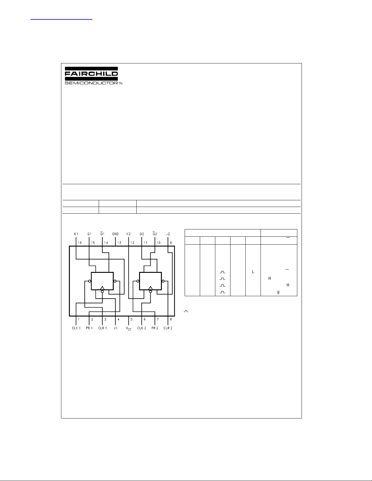
This device contains two inde pendent positive pulse triggered J-K flip-flops with complementary outputs. The J and
K data is processed by the flip-flo p after a complete clock
pulse. While the clock is LOW the slave is isolated from the
master. On the positive transition of the clock, the data
from the J and K inputs is tra nsferred to the master. While
the clock is HIGH the J and K inpu ts are disabled. On the
negative transition of the clock, the data from the ma ster i s
transferred to t he slave. The logic state of J and K in puts
must not be allowed to change w hile the clock is HIGH.
The data is transferred to the outputs on the falling edge of
the clock pulse. A LOW logic le vel on the preset or clear
inputs will set or reset the outputs regardless of the logic
levels of the other inputs.
Ordering Code:
Order Number Package Number Package Description
DM7476N N16E 16-Lead Plastic Dual-In-Line Package (PDIP), JEDEC MS-001, 0.300 Wide
Connection Diagram Function Table
Inputs Outputs
PR CLR CLK J K Q Q
LHXXX H L
HLXXX L H
LLXXXH
HH
HH
HH
HH
H = HIGH Logic Level
L = LOW Logic Level
X = Either LOW or HIGH Logic Level
= Positive pulse data. The J and K inputs must be held constant while
the clock is HIGH. D ata is transferred to the outpu ts on the falling
edge of the clock pulse.
= The output logic level befor e the indicated input conditions were
Q
0
established.
Toggle = Each output changes to the complement of its previous level on
each complete active HIGH level clock pulse.
Note 1: This configuration is n onstabl e; tha t is, it will not pe rsist wh en the
preset and/or clear inputs return to their inac t iv e (H I GH) level.
LLQ0Q
HL H L
LH L H
H H Toggle
(Note 1)H(Note 1)
0
© 2000 Fairchild Semiconductor Corporation DS006528 www.fairchildsemi.com
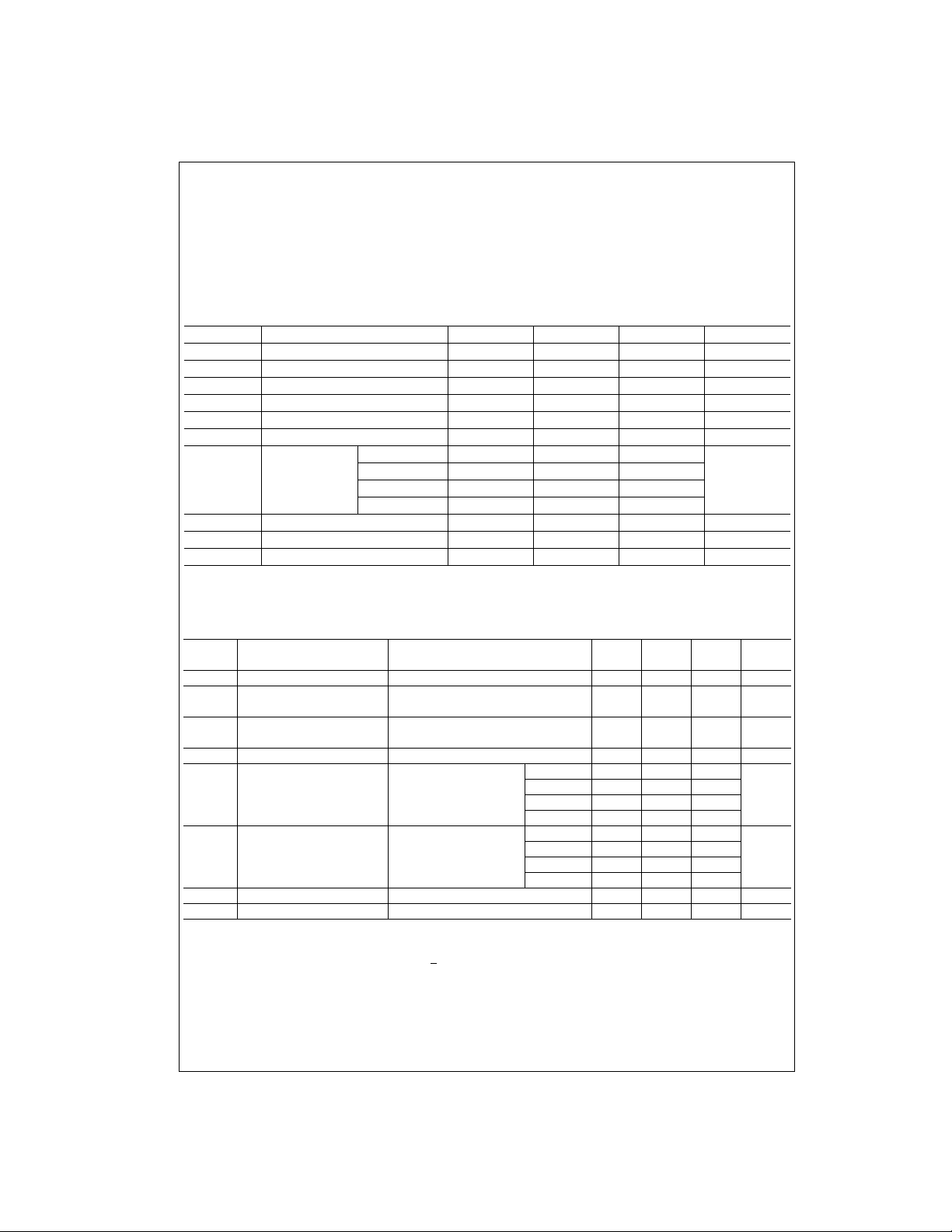
Absolute Maximum Ratings(Note 2)
Supply Voltage 7V
DM7476
Input Voltage 5.5V
Operating Free Air Temperature Range 0°C to +70°C
Storage Temperature Range −65°C to +150°C
Note 2: The “Absolute Maximum Ratin gs” are those v alues beyon d which
the safety of the dev ice cannot be guaranteed. T he device sh ould not be
operated at these limits. The parametric values defined in the Electrical
Characteristics tables are not guaranteed at the absolute maximum ratings.
The “Recommend ed O peratin g Cond itions” t able w ill defin e the c ondit ions
for actual device operation.
Recommended Operating Conditions
Symbol Parameter Min Nom Max Units
V
V
V
I
I
f
t
CC
IH
IL
OH
OL
CLK
W
Supply Voltage 4.75 5 5.25 V
HIGH Level Input Voltage 2 V
LOW Level Input Voltage 0.8 V
HIGH Level Output Current −0.4 mA
LOW Level Output Current 16 mA
Clock Frequency (Note 3) 0 15 MHz
Pulse Width Clock HIGH 20
(Note 3) Clock LOW 47
Preset LOW 25
Clear LOW 25
t
SU
t
H
T
A
Note 3: TA = 25°C and VCC = 5V.
Note 4: The symbol (↑, ↓) indicates the edge of the cl oc k pulse is used for referenc e (↑) for rising edge, (↓) for falling edge .
Input Setup Time (Note 3)(Note 4) 0↑ ns
Input Hold Time (Note 3)(Note 4) 0↓ ns
Free Air Operating Temperature 0 70 °C
Electrical Characteristics
over recommended operating free air temperature range (unless otherwise noted)
Symbol Parameter Conditions Min
V
I
V
OH
V
OL
I
I
I
IH
I
IL
I
OS
I
CC
Note 5: All typicals are at VCC = 5V, TA = 25°C.
Note 6: Clear is measured with preset HIGH and preset is measured with clear HIGH.
Note 7: Not more than one output should be shorted at a time.
Note 8: With all outputs OPEN, I
Input Clamp Voltage VCC = Min, II = −12 mA −1.5 V
HIGH Level VCC = Min, IOH = Max
Output Voltage VIL = Max, VIH = Min
LOW Level VCC = Min, IOL = Max
Output Voltage VIH = Min, VIL = Max
Input Current @ Max Input Voltage VCC = Max, VI = 5.5V 1 mA
HIGH Level VCC = Max J, K 40
Input Current VI = 2.4V Clock 80
LOW Level VCC = Max J, K −1.6
Input Current VI = 0.4V Clock −3.2
(Note 6) Clear −3.2
Short Circuit Output Current VCC = Max (Note 7) −18 −55 mA
Supply Current VCC = Max (Note 8) 18 34 mA
is measured with the Q and Q outputs HIGH in turn. At the t im e of m easurement the clock input is grounded.
CC
Clear 80
Preset 80
Preset −3.2
2.4 3.4 V
Typ
(Note 5)
0.2 0.4 V
ns
Max Units
µA
mA
www.fairchildsemi.com 2
 Loading...