

National Semiconductor 5442A, DM5442A, DM7442A Technical data
查询5442ADMQB供应商
5442A/DM5442A/DM7442A
BCD to Decimal Decoders
5442A/DM5442A/DM7442A BCD to Decimal Decoders
June 1989
General Description
These BCD-to-decimal decoders consist of eight inverters
and ten, four-input NAND gates. The inverters are connected in pairs to make BCD input data available for decoding
by the NAND gates. Full decoding of input logic ensures
that all outputs remain off for all invalid (10 –15) input conditions.
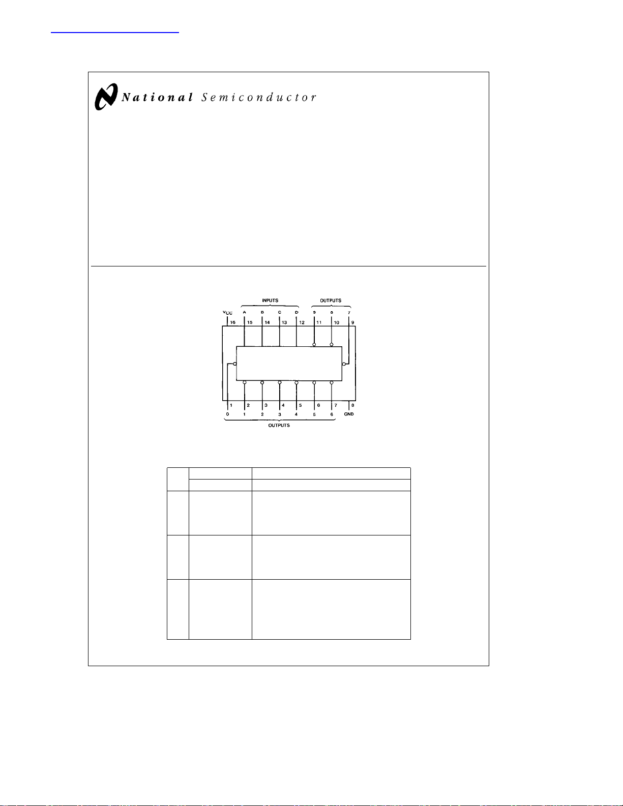
Connection Diagram
Dual-In-Line Package
Order Number 5442ADMQB, 5442AFMQB, DM5442AJ, DM5442AW or DM7442AN
See NS Package Number J16A, N16E or W16A
Function Table
No.
HeHigh Level
e
L
BCD Input Decimal Output
DCBA0123456789
0 L L L L LHHHHHHHHH
1 L L L HHL HHHHHHHH
2 L L HL HHL HHHHHHH
3 L L HHHHHL HHHHHH
4 LHL L HHHHL HHHHH
5 LHL HHHHHHL HHHH
6 LHHLHHHHHHLHHH
7 LHHHHHHHHHHL HH
8 H L L LHHHHHHHHL H
9 H L LHHHHHHHHHHL
I H LHL HHHHHHHHHH
N H LHHHHHHHHHHHH
V HHLLHHHHHHHHHH
A HHL HHHHHHHHHHH
L HHH LHHHHHHHHHH
I HHHHHHHHHHHHHH
D
Low Level
Features
Y
Diode clamped inputs
Y
Also for application as 4-line-to-16-line decoders; 3-lineto-8-line decoders
Y
All outputs are high for invalid input conditions
Y
Typical power dissipation 140 mW
Y
Typical propagation delay 17 ns
Y
Alternate Military/Aerospace device (5442A) is available. Contact a National Semiconductor Sales Office/
Distributor for specifications.
TL/F/6516– 1
C
1995 National Semiconductor Corporation RRD-B30M105/Printed in U. S. A.
TL/F/6516
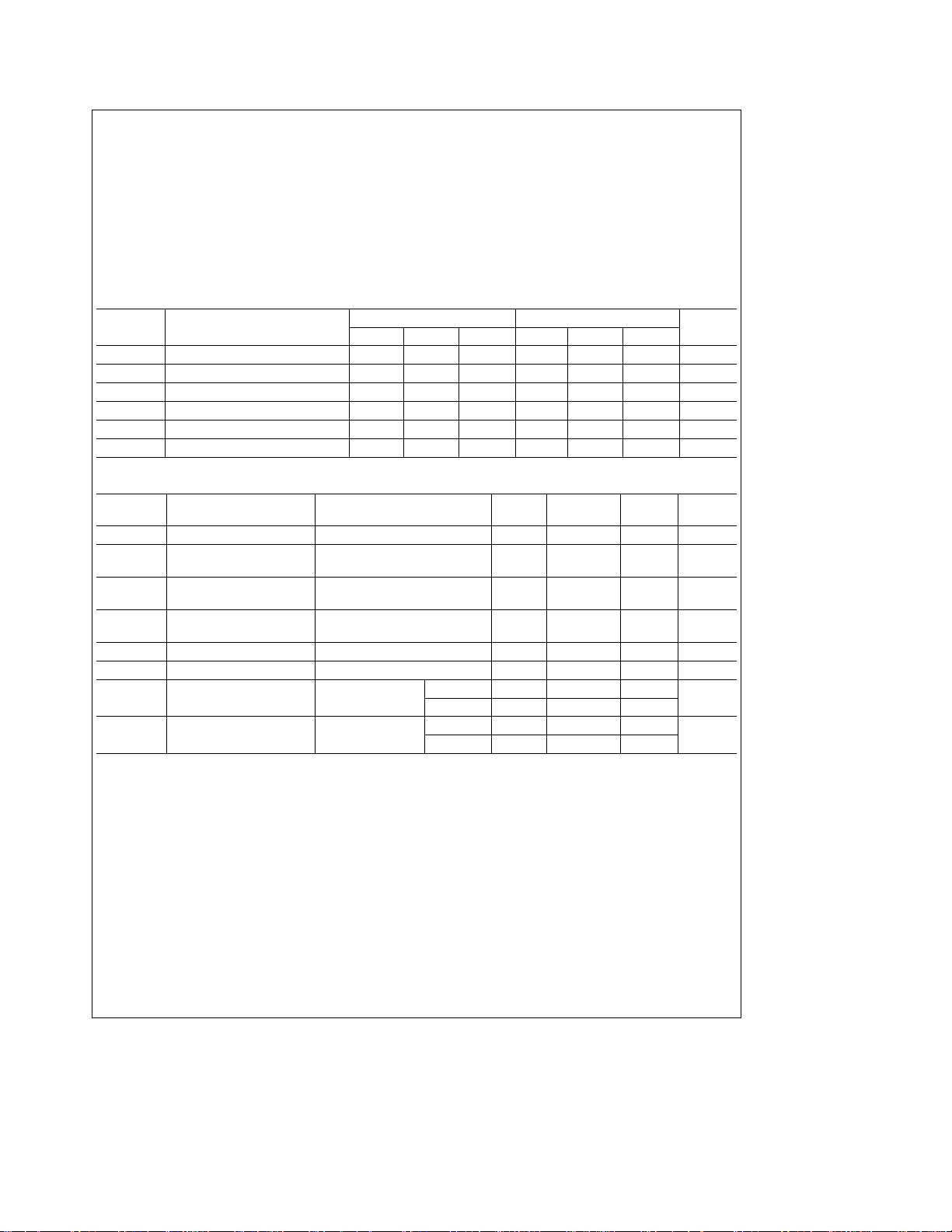
Absolute Maximum Ratings (Note)
The ‘‘Absolute Maximum Ratings’’ are those values
If Military/Aerospace specified devices are required,
please contact the National Semiconductor Sales
Office/Distributors for availability and specifications.
Supply Voltage 7V
Input Voltage 5.5V
Operating Free Air Temperature Range
DM54 and 54
DM74 0
Storage Temperature Range
b
55§Ctoa125§C
Ctoa70§C
§
b
65§Ctoa150§C
Note:
beyond which the safety of the device cannot be guaranteed. The device should not be operated at these limits. The
parametric values defined in the ‘‘Electrical Characteristics’’
table are not guaranteed at the absolute maximum ratings.
The ‘‘Recommended Operating Conditions’’ table will define
the conditions for actual device operation.
Recommended Operating Conditions
Symbol Parameter
V
CC
V
IH
V
IL
I
OH
I
OL
T
A
Supply Voltage 4.5 5 5.5 4.75 5 5.25 V
High Level Input Voltage 2 2 V
Low Level Input Voltage 0.8 0.8 V
High Level Output Current
Low Level Output Current 16 16 mA
Free Air Operating Temperature
DM5442A DM7442A
Min Nom Max Min Nom Max
b
0.8
b
55 125 0 70
b
Units
0.8 mA
Electrical Characteristics over recommended operating free air temperature range (unless otherwise noted)
Symbol Parameter Conditions Min
e
V
I
V
OH
V
OL
I
I
I
IH
I
IL
I
OS
I
CC
Note 1: All typicals are at V
Note 2: Not more than one output should be shorted at a time.
Note 3: I
Input Clamp Voltage V
High Level Output V
Voltage V
Low Level Output V
Voltage V
Input Current@Max V
Input Voltage
High Level Input Current V
Low Level Input Current V
Short Circuit V
Output Current (Note 2)
Supply Current V
e
e
5V, T
CC
is measured with all outputs open and all inputs grounded.
CC
25§C.
A
CC
CC
IL
CC
IH
CC
CC
CC
CC
CC
(Note 3)
e
e
eb
Min, I
e
Min, I
Max, V
e
Min, I
Min, V
e
Max, V
e
Max, V
e
Max, V
e
Max DM54
e
Max DM54 28 41
12 mA
I
e
Max
OH
e
Min
IH
e
Max
OL
e
Max
IL
e
5.5V
I
e
2.4V 40 mA
I
e
0.4V
I
DM74
2.4 3.4 V
b
b
DM74 28 56
20
18
Typ
(Note 1)
Max Units
b
1.5 V
0.2 0.4 V
1mA
b
1.6 mA
b
55
b
55
§
mA
mA
C
2
 Loading...