

查询74185供应商
DM74184/DM74185A
BCD-to-Binary and Binary-to-BCD Converters
General Description
These monolithic converters are derived from the 256-bit
read only memories, DM5488, and DM7488. Emitter connections are made to provide direct read-out of converted
codes at outputs Y8 through Y1, as shown in the function
tables. These converters demonstrate the versatility of a
read only memory in that an unlimited number of reference
tables or conversion tables may be built into a system. Both
of these converters comprehend that the least significant
bits (LSB) of the binary and BCD codes are logically equal,
and in each case the LSB bypasses the converter as illustrated in the typical applications. This means that a 6-bit
converter is produced in each case. Both devices are cascadable to N bits.
An overriding enable input is provided on each converter
which when taken high inhibits the function, causing all outputs to go high. For this reason, and to minimize power
consumption, unused outputs Y7 and Y8 of the 185A and all
‘‘don’t care’’ conditions of the 184 are programmed high.
The outputs are of the open-collector type.
DM74184 BCD-TO-BINARY CONVERTERS
The 6-bit BCD-to-binary function of the DM74184 is analogous to the algorithm:
a. Shift BCD number right one bit and examine each dec-
ade. Subtract three from each 4-bit decade containing a
binary value greater than seven.
DM74184/DM74185A BCD-to-Binary and Binary-to-BCD Converters
June 1989
b. Shift right, examine, and correct after each shift until the
least significant decade contains a number smaller than
eight and all other converted decades contain zeros.
In addition to BCD-to-binary conversion, the DM74184 is
programmed to generate BCD 9’s complement or BCD 10’s
complement. Again, in each case, one bit of the complement code is logically equal to one of the BCD bits; therefore, these complements can be produced on three lines.
As outputs Y6, Y7 and Y8 are not required in the BCD-to-binary conversion, they are utilized to provide these complement codes as specified in the function table when the devices are connected as shown.
DM74185A BINARY-TO-BCD CONVERTERS
The function performed by these 6-bit binary-to-BCD converters is analogous to the algorithm:
a. Examine the three most significant bits. If the sum is
greater than four, add three and shift left one bit.
b. Examine each BCD decade. If the sum is greater than
four, add three and shift left one bit.
c. Repeat step b until the least-significant binary bit is in the
least-significant BCD location.
(Continued)
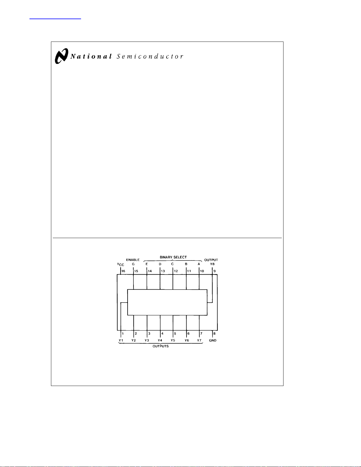
Connection Diagram
Order Number DM74184N or DM74185AN
See NS Package Number N16E
C
1995 National Semiconductor Corporation RRD-B30M105/Printed in U. S. A.
TL/F/6561
TL/F/6561– 1
Absolute Maximum Ratings (Note)
Note:
If Military/Aerospace specified devices are required,
please contact the National Semiconductor Sales
Office/Distributors for availability and specifications.
Supply Voltage 7V
Input Voltage 5.5V
Output Voltage 7V
Operating Free Air Temperature
Range 0
Storage Temperature Range
Ctoa70§C
§
b
65§Ctoa150§C
The ‘‘Absolute Maximum Ratings’’ are those values
beyond which the safety of the device cannot be guaranteed. The device should not be operated at these limits. The
parametric values defined in the ‘‘Electrical Characteristics’’
table are not guaranteed at the absolute maximum ratings.
The ‘‘Recommended Operating Conditions’’ table will define
the conditions for actual device operation.
Recommended Operating Conditions
Symbol Parameter Min Nom Max Units
V
CC
V
IH
V
IL
V
OH
I
OL
T
A
Supply Voltage 4.75 5 5.25 V
High Level Input Voltage 2 V
Low Level Input Voltage 0.8 V
High Level Output Voltage 5.5 V
Low Level Output Current 12 mA
Free Air Operating Temperature 0 70
’184 and ’185A Electrical Characteristics
over recommended operating free air temperature range (unless otherwise noted)
Symbol Parameter Conditions Min
e
e
Max, V
e
Min, V
e
e
e
e
e
Min, I
Min, V
Min, I
Max, V
Max, V
Max, V
Max
Max
eb
12 mA
I
e
5.5V
O
e
Min
IH
e
Max
OL
e
Max
IL
e
5.5V
I
e
2.4V 25 mA
I
e
0.4V
I
V
I
I
CEX
V
OL
I
I
I
IH
I
IL
I
CCH
I
CCL
Input Clamp Voltage V
High Level Output V
Current V
Low Level Output V
Voltage V
Input Current@Max V
Input Voltage
High Level Input Current V
Low Level Input Current V
Supply Current with V
Outputs High
Supply Current with V
Outputs Low
CC
CC
IL
CC
IH
CC
CC
CC
CC
CC
e
e
Typ
(Note 1)
Max Units
b
1.5 V
100 mA
0.4 V
1mA
b
1mA
65 95 mA
80 99 mA
C
§
’184 and ’185A Switching Characteristics
e
at V
CC
5V and T
Symbol Parameter To (Output)
t
PLH
t
PHL
t
PLH
t
PHL
Note 1: All typicals are at V
e
25§C (See Section 1 for Test Waveforms and Output Load)
A
From (Input)
Propagation Delay Time Enable G
Low to High Level Output to Output
Propagation Delay Time Enable G
High to Low Level Output to Output
Propagation Delay Time Binary Select
Low to High Level Output to Output
Propagation Delay Time Binary Select
High to Low Level Output to Output
e
e
5V, T
CC
25§C.
A
2
e
400X,R
R
L1
e
15 pF (See Test Circuit)
C
L
e
L2
Min Max
600X
Units
35 ns
35 ns
35 ns
35 ns
General Description (Continued)
TABLE I. Package Count and Delay Times
Input Packages Total Delay Times (ns)
(Decades) Required
2 2 56 80
3 6 140 200
4 12 196 280
5 19 280 400
6 28 364 520
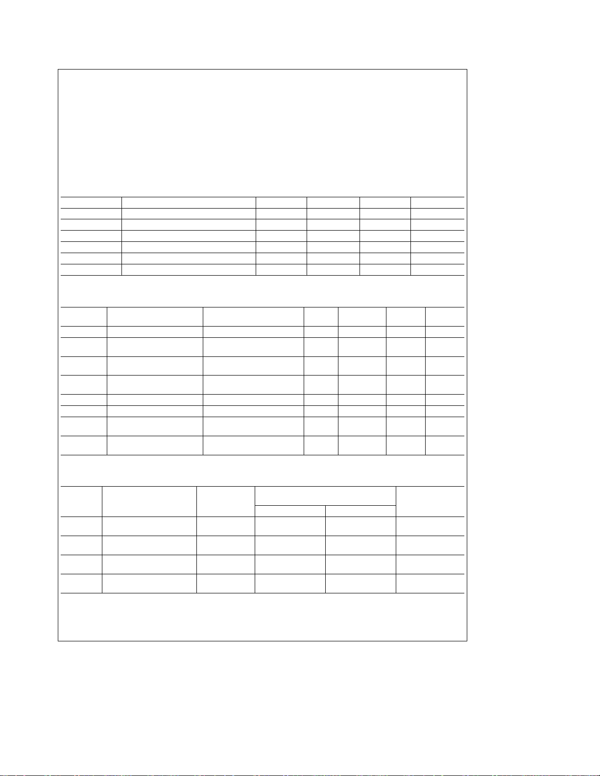
DM74184 BCD-to-Binary
for BCD-to-Binary Conversion
Typ Max
6-Bit Converter
BCD 9’s
Complement Converter
TL/F/6561– 2
DM74185A Binary-to-BCD
TABLE II. Package Count and Delay Times
for Binary-to-BCD Conversion
Input Packages Total Delay Times (ns)
(Bits) Required
Typ Max
4to6 1 25 40
7or8 3 50 80
9 4 75 120
10 6 100 160
11 7 125 200
12 8 125 200
13 10 150 240
14 12 175 280
15 14 175 280
16 16 200 320
17 19 225 360
18 21 225 360
19 24 250 400
20 27 275 440
TL/F/6561– 3
BCD’s 10’s
Complement Converter
TL/F/6561– 4
6-Bit Converter
TL/F/6561– 5
3

Function Tables
Binary
Words Binary Select Enable
EDCBA G Y8Y7Y6Y5Y4Y3Y2Y1
01LLLLL L HHLLLLLL
23LLLLH L HHLLLLLH
45LLLHL L HHLL LLHL
67LLLHH L HHLLLLHH
89LLHLL L HHLL LHLL
10 11 L L H L H L H H L L H L L L
1213LLHHL L HHLLHLLH
1415LLHHH L HHLLHLHL
1617LHLLL L HHLLHLHH
1819LHLLH L HHLLHHLL
2021LHLHL L HHLHLLLL
22 23 L H L H H L H H L H L L L H
2425LHHLL L HHLHLLHL
2627LHHLH L HHLHLLHH
2829LHHHL L HHLHLHLL
30 31 L H H H H L H H L H H L L L
3233HLLLL L HHLHHLLH
3435HLLLH L HHLHHLHL
3637HLLHL L HHLHHLHH
38 39 H L L H H L H H L H H H L L
4041HLHLL L HHHLLLLL
4243HLHLH L HHHLLLLH
4445HLHHL L H H H L L L H L
4647HLHHH L HHHL L LHH
48 49 H H L L L L H H H L L H L L
50 51 H H L L H L H H H L H L L L
5253HHLHL L HHHLHLLH
5455HHLHH L HHHLHLHL
5657HHHLL L HHHLHLHH
5859HHHLH L HHHLHHL L
6061HHHHL L HHHHLLLL
6263HHHHH L HHHH L L L H
All XXXXX H HHHHHHHH
Inputs Outputs
4

Function Tables (Continued)
BCD-to-Binary Converter
BCD
Words
Inputs Outputs
(See Note A) (See Note B)
EDCBAGY5Y4Y3Y2Y1
0 1 LLLLLL L L L L L
2 3 LLLLHL L L L L H
4 5 LLLHL L L L L H L
67LLLHHLLLLHH
89LLHLLLLLHLL
10 11 L H L L L L L L H L H
12 13 L H L L H L L L H H L
14 15 LHLHLL L L H H H
16 17 L H L H H L L H L L L
18 19 L H H L L L L H L L H
20 21 H L L L L L L H L H L
22 23 H L L L H L L H L H H
24 25 HL LHLL L H H L L
26 27 HLLHHLLHHLH
28 29 H L H L L L L H H H L
30 31 H H L L L L L H H H H
32 33 H H L L H L H L L L L
34 35 H H L H L L H L L L H
36 37 HHLHHLHL LHL
38 39 H H H L L L H L L H H
Any XXXXXH H H H H H
HeHigh Level, LeLow Level, XeDon’t Care
Note A: Input Conditions other than those shown produce highs at outputs Y1 through Y5.
Note B: Output Y6, Y7, and Y8 are not used for BCD-to-Binary conversion.
Note C: Input conditions other than those shown produce highs at outputs Y6, Y7, and Y8.
Note D: Outputs Y1 through Y5 are not used for BCD 9’s or BCD 10’s complement conversion.
²
When these devices are used as complement converters, input E is used as a mode control. With this input low, the BCD 9’s complement is generated; when it is
high, the BCD 10’s complement is generated.
BCD 9’s or BCD 10’s Complement Converter
BCD
Word
Inputs Outputs
(See Note C) (See Note D)
E²DCBAGY8Y7Y6
0 L LLLLL H L H
1 L LLLHL H L L
2 L LLHLL L H H
3 LLLHHLLHL
4 L LHLLL L H H
5 L LHLHL L H L
6 L LHHLL L L H
7 L L HHHL L L L
8 L HLLLL L L H
9 L HL LHL L L L
0 H LLLLL L L L
1 H LLLHL H L L
2 H L LHL L H L L
3HLLHHLLHH
4 H LHL L L L H H
5 H LHLHL L H L
6 H LHHLL L H L
7 H LHHHL L L H
8 HHLLLL L L H
9 H HLLHL L L L
Any X XXXXH H H H
Test Circuit
CLincludes probe and jig capacitance
TL/F/6561– 6
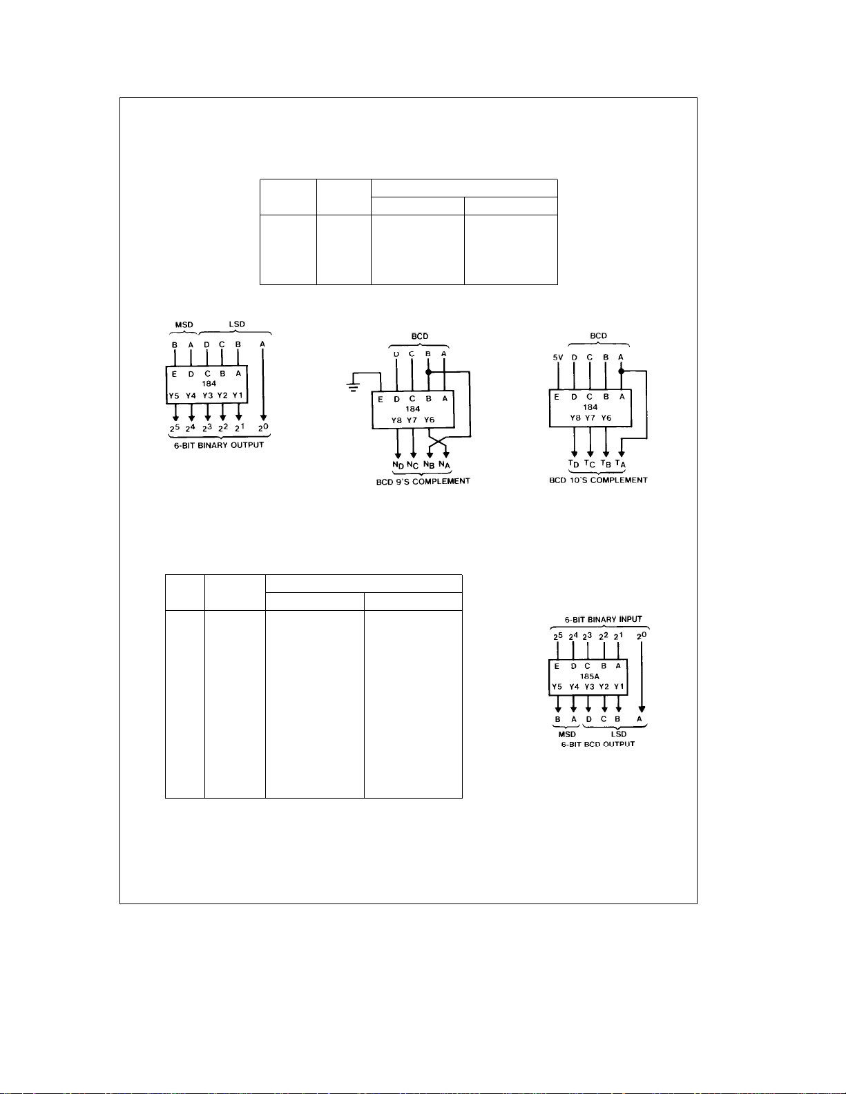
Typical Applications
FIGURE 1. BCD-to-Binary Converter
MSDÐMost significant decade
LSDÐLeast significant decade
Each rectangle represents a DM74184
5
for Two BCD Decades
TL/F/6561– 7

Typical Applications (Continued)
MSDÐMost significant decade
LSDÐLeast significant decade
Each rectangle represents a DM74184
FIGURE 2. BCD-to-Binary Converter for Six BCD Decades
TL/F/6561– 9
6

Typical Applications (Continued)
FIGURE 3. BCD-to-Binary Converter
for Three BCD Decades
MSDÐMost significant decade
LSDÐLeast significant decade
Each rectangle represents a DM74184
TL/F/6561– 8
FIGURE 4. 6-Bit Binary-to-BCD Converter
MSDÐMost significant decade
LSDÐLeast significant decade
Note A: Each rectangle represents a DM74185A.
Note B: All unused E inputs are grounded.
TL/F/6561– 10
FIGURE 5. 8-Bit Binary-to-BCD Converter
MSDÐMost significant decade
LSDÐLeast significant decade
Note A: Each rectangle represents a DM74185A.
Note B: All unused E inputs are grounded.
TL/F/6561– 11
FIGURE 6. 9-Bit Binary-to-BCD Converter
TL/F/6561– 12
MSDÐMost significant decade
LSDÐLeast significant decade
Note A: Each rectangle represents a DM74185A.
Note B: All unused E inputs are grounded.
7
Typical Applications (Continued)
FIGURE 7. 12-Bit Binary-to-BCD
Converter (See Note B)
MSDÐMost significant decade
LSDÐLeast significant decade
Note A: Each rectangle represents a DM74185A.
Note B: All unused E inputs are grounded.
TL/F/6561– 13
TL/F/6561– 14
FIGURE 8. 16-Bit Binary-to-BCD Converter (See Note B)
8

9

Physical Dimensions inches (millimeters)
16-Lead Molded Dual-In-Line Package (N)
Order Number DM74184N or DM74185AN
NS Package Number N16E
DM74184/DM74185A BCD-to-Binary and Binary-to-BCD Converters
LIFE SUPPORT POLICY
NATIONAL’S PRODUCTS ARE NOT AUTHORIZED FOR USE AS CRITICAL COMPONENTS IN LIFE SUPPORT
DEVICES OR SYSTEMS WITHOUT THE EXPRESS WRITTEN APPROVAL OF THE PRESIDENT OF NATIONAL
SEMICONDUCTOR CORPORATION. As used herein:
1. Life support devices or systems are devices or 2. A critical component is any component of a life
systems which, (a) are intended for surgical implant support device or system whose failure to perform can
into the body, or (b) support or sustain life, and whose be reasonably expected to cause the failure of the life
failure to perform, when properly used in accordance support device or system, or to affect its safety or
with instructions for use provided in the labeling, can effectiveness.
be reasonably expected to result in a significant injury
to the user.
National Semiconductor National Semiconductor National Semiconductor National Semiconductor
Corporation Europe Hong Kong Ltd. Japan Ltd.
1111 West Bardin Road Fax: (
Arlington, TX 76017 Email: cnjwge@tevm2.nsc.com Ocean Centre, 5 Canton Rd. Fax: 81-043-299-2408
Tel: 1(800) 272-9959 Deutsch Tel: (
Fax: 1(800) 737-7018 English Tel: (
National does not assume any responsibility for use of any circuitry described, no circuit patent licenses are implied and National reserves the right at any time without notice to change said circuitry and specifications.
Fran3ais Tel: (
Italiano Tel: (
a
49) 0-180-530 85 86 13th Floor, Straight Block, Tel: 81-043-299-2309
a
49) 0-180-530 85 85 Tsimshatsui, Kowloon
a
49) 0-180-532 78 32 Hong Kong
a
49) 0-180-532 93 58 Tel: (852) 2737-1600
a
49) 0-180-534 16 80 Fax: (852) 2736-9960
 Loading...