

National Semiconductor 54121, DM54121, DM74121 Technical data
54121/DM54121/DM74121 One-Shot with
Clear and Complementary Outputs
Y
General Description
The DM54/74121 is a monostable multivibrator featuring
both positive and negative edge triggering with complementary outputs. An internal 2kX timing resistor is provided for
design convenience minimizing component count and layout problems. This device can be used with a single external
capacitor. Inputs (A) are active-low trigger transition inputs
and input (B) is an active-high transition Schmitt-trigger input that allows jitter-free triggering from inputs with transition rates as slow as 1 volt/second. A high immunity to
V
noise of typically 1.5V is also provided by internal cir-
CC
cuitry at the input stage.
To obtain optimum and trouble free operation please read
operating rules and NSC one-shot application notes carefully and observe recommendations.
Features
Y
Triggered from active-high transition or active-low transition inputs
Y
Variable pulse width from 30 ns to 28 seconds
Jitter free Schmitt-trigger input
Y
Excellent noise immunity typically 1.2V
Y
Stable pulse width up to 90% duty cycle
Y
TTL, DTL compatible
Y
Compensated for VCCand temperature variations
Y
Input clamp diodes
Y
Alternate Military/Aerospace device (54121) is available. Contact a National Semiconductor Sales Office/
Distributor for specifications.
Functional Description
The basic output pulse width is determined by selection of
an internal resistor R
capacitor (C
dependent of further transitions of the inputs and is a function of the timing components. Pulse width can vary from a
few nano-seconds to 28 seconds by choosing appropriate
R
and CXcombinations. There are three trigger inputs from
X
the device, two negative edge-triggering (A) inputs, one positive edge Schmitt-triggering (B) input.
). Once triggered the output pulse width is in-
X
or an external resistor (RX) and
INT
54121/DM54121/DM74121 One-Shot with Clear and Complementary Outputs
June 1989
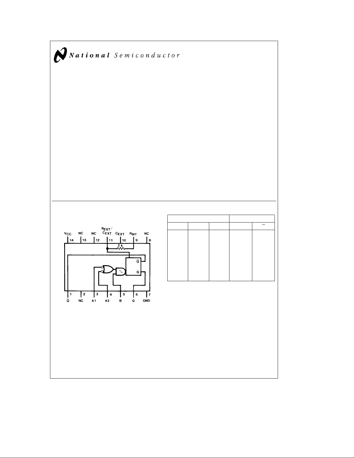
Connection Diagram
Dual-In-Line Package
Order Number 54121DMQB, 54121FMQB,
DM54121J, DM54121W or DM74121N
See NS Package Number J14A, N14A or W14B
TL/F/6538– 1
Function Table
Inputs Outputs
A1 A2 B Q Q
LXHL H
XLH L H
XXL L H
HHX L H
H
v
vv
LX
XL
e
H
High Logic Level
e
L
Low Logic Level
e
X
Can Be Either Low or High
e
Positive Going Transition
u
e
Negative Going Transition
v
e
É
A Positive Pulse
e
ß
A Negative Pulse
v
HHÉß
HÉß
H Éß
u
u
Éß
Éß
C
1995 National Semiconductor Corporation RRD-B30M105/Printed in U. S. A.
TL/F/6538
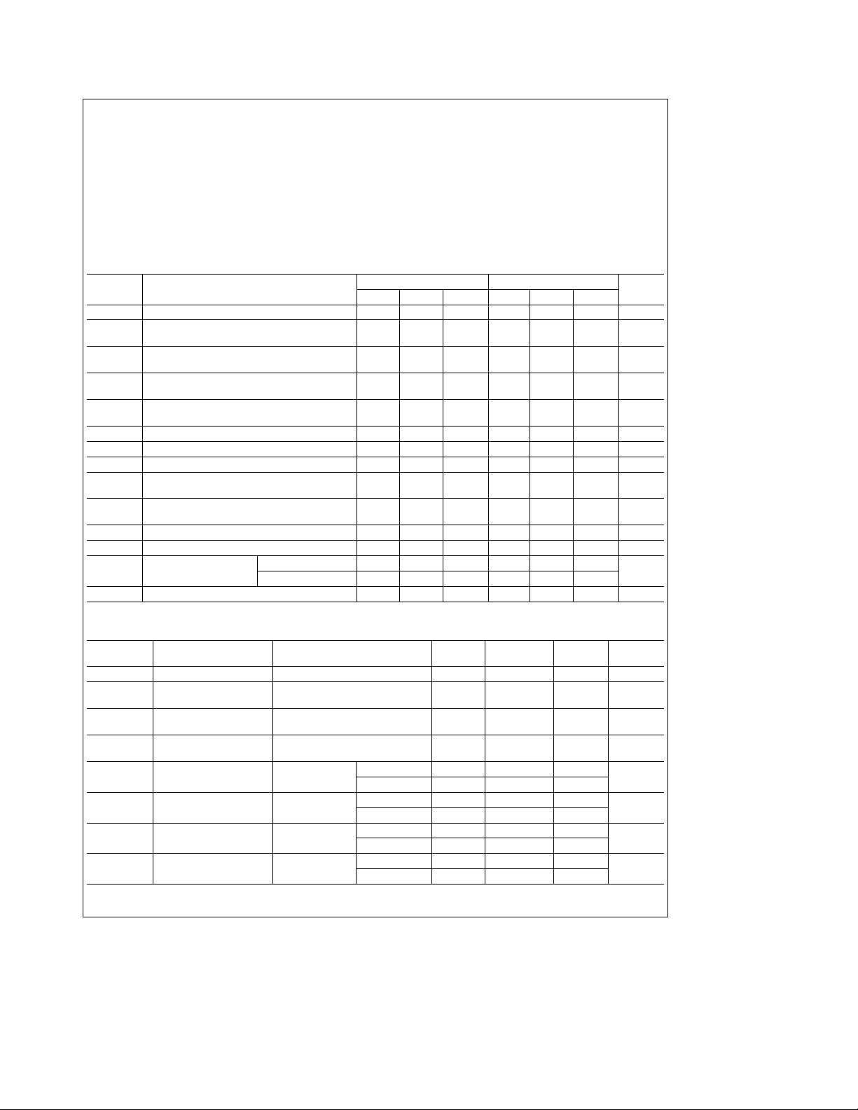
Absolute Maximum Ratings (Note)
The ‘‘Absolute Maximum Ratings’’ are those values
If Military/Aerospace specified devices are required,
please contact the National Semiconductor Sales
Office/Distributors for availability and specifications.
Supply Voltage 7V
Input Voltage 5.5V
Operating Free Air Temperature Range
DM54
DM74 0
Storage Temperature Range
b
55§Ctoa125§C
Ctoa70§C
§
b
65§Ctoa150§C
Note:
beyond which the safety of the device cannot be guaranteed. The device should not be operated at these limits. The
parametric values defined in the ‘‘Electrical Characteristics’’
table are not guaranteed at the absolute maximum ratings.
The ‘‘Recommended Operating Conditions’’ table will define
the conditions for actual device operation.
Recommended Operating Conditions
Symbol Parameter
V
CC
V
a
T
V
b
T
V
a
T
V
b
T
I
OH
I
OL
t
W
dV/dt
dV/dt
R
EXT
C
EXT
Supply Voltage 4.5 5 5.5 4.75 5 5.25 V
Positive-Going Input Threshold
Voltage at the A Input (V
Negative-Going Input Threshold
Voltage at the A Input (V
Positive-Going Input Threshold
Voltage at the B Input (V
Negative-Going Input Threshold
Voltage at the B Input (V
CC
CC
CC
CC
High Level Output Current
Low Level Output Current 16 16 mA
Input Pulse Width (Note 1) 40 40 ns
Rate of Rise or Fall of
Schmidt Input (B) (Note 1)
Rate of Rise or Fall of
Logic Input (A) (Note 1)
External Timing Resistor (Note 1) 1.4 30 1.4 40 kX
External Timing Capacitance (Note 1) 0 1000 0 1000 mF
DC Duty Cycle (Note 1) R
T
A
Note 1: T
Free Air Operating Temperature
e
A
25§C and V
e
5V.
CC
e
Min)
e
Min)
e
Min)
e
Min)
e
2kX 67 67
T
e
R
R
T
(Max) 90 90
EXT
DM54121 DM74121
Min Nom Max Min Nom Max
1.4 2 1.4 2 V
0.8 1.4 0.8 1.4 V
1.5 2 1.5 2 V
0.8 1.3 0.8 1.3 V
b
0.4
b
0.4 mA
1 1 V/s
11V/ms
b
55 125 0 70
Electrical Characteristics over recommended operating free air temperature range (unless otherwise noted)
Symbol Parameter Conditions Min
e
V
I
V
OH
V
OL
I
I
I
IH
I
IL
I
OS
I
CC
Input Clamp Voltage V
High Level Output V
Voltage V
Low Level Output V
Voltage V
Input Current@Max V
Input Voltage
High Level Input V
Current V
Low Level Input V
Current V
Short Circuit V
Output Current (Note 2)
Supply Current V
CC
CC
IL
CC
IH
CC
CC
I
CC
I
CC
CC
e
e
e
e
eb
Min, I
e
Min, I
Max, V
e
Min, I
Min, V
e
Max, V
e
Max A1, A2 40
2.4V
e
Max A1, A2
0.4V
e
Max DM54
e
Max Quiescent 13 25
12 mA
I
e
Max,
OH
e
Min
IH
e
Max,
OL
e
Max
IL
e
5.5V
I
B80
B
b
DM74
b
Triggered 23 40
e
Note 1: All typicals are at V
Note 2: Not more than one output should be shorted at a time.
CC
5V, T
e
25§C.
A
2.4 3.4 V
20
18
Typ
(Note 1)
Max Units
b
1.5 V
0.2 0.4 V
1mA
b
1.6
b
3.2
b
55
b
55
Units
%
C
§
mA
mA
mA
mA
2
 Loading...