

查询DAC1218供应商
DAC1218/DAC1219
12-Bit Binary Multiplying D/A Converter
General Description
The DAC1218 and the DAC1219 are 12-bit binary, 4-quadrant multiplying D to A converters. The linearity, differential
non-linearity and monotonicity specifications for these converters are all guaranteed over temperature. In addition,
these parameters are specified with standard zero and fullscale adjustment procedures as opposed to the impractical
best fit straight line guarantee.
This level of precision is achieved though the use of an
advanced silicon-chromium (SiCr) R-2R resistor ladder network. This type of thin-film resistor eliminates the parasitic
diode problems associated with diffused resistors and allows the applied reference voltage to range from
25V, independent of the logic supply voltage.
CMOS current switches and drive circuitry are used to
achieve low power consumption (20 mW typical) and minimize output leakage current errors (10 nA maximum).
Unique digital input circuitry maintains TTL compatible input
threshold voltages over the full operating supply voltage
range.
The DAC1218 and DAC1219 are direct replacements for
the AD7541 series, AD7521 series, and AD7531 series with
a significant improvement in the linearity specification. In
applications where direct interface of the D to A converter to
b
25V to
December 1994
a microprocessor bus is desirable, the DAC1208 and
DAC1230 series eliminate the need for additional interface
logic.
Features
Y
Linearity specified with zero and full-scale adjust only
Y
Logic inputs which meet TTL voltage level specs (1.4V
logic threshold)
Y
Works withg10V referenceÐfull 4-quadrant
multiplication
Y
All parts guaranteed 12-bit monotonic
Key Specifications
Y
Current Settling Time 1 ms
Y
Resolution 12 Bits
Y
Linearity (Guaranteed 12 Bits (DAC1218)
over temperature) 11 Bits (DAC1219)
Y
Gain Tempco 1.5 ppm/§C
Y
Low Power Dissipation 20 mW
Y
Single Power Supply 5 VDCto 15 V
DC
DAC1218/DAC1219 12-Bit Binary Multiplying D/A Converter
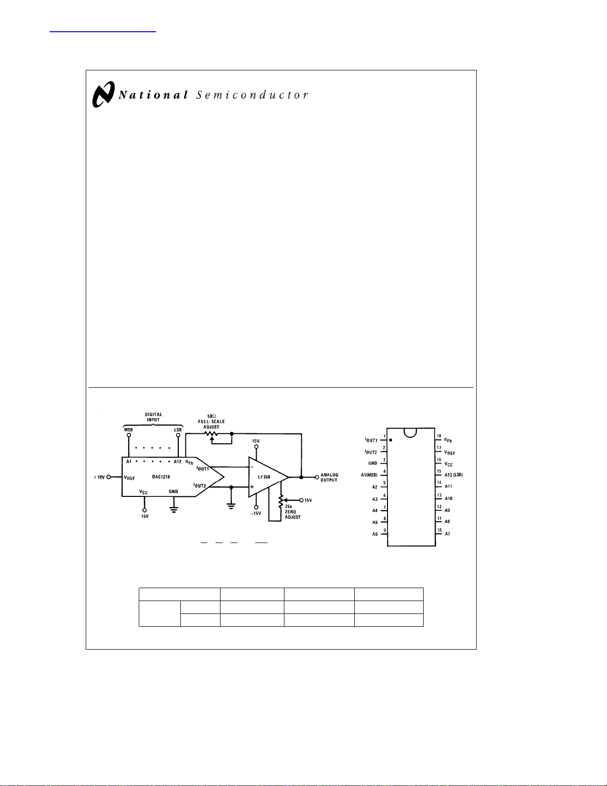
Typical Application
Connection Diagram
Dual-In-Line Package
A1
A2
eb
V
V
OUT
REF
#
where: ANe1 if digital input is high
e
AN
0 if digital input is low
A3
a
a
2
4
8
A12
a
...
4096
J
TL/H/5691– 1
TL/H/5691– 15
Top View
Ordering Information
Temperature Range 0§Ctoa70§C
Non 0.012% DAC1218LCJ-1 DAC1218LCJ J18A Cerdip
Linearity
BI-FETTMis a trademark of National Semiconductor Corp.
C
1995 National Semiconductor Corporation RRD-B30M115/Printed in U. S. A.
0.024% DAC1219LCJ J18A Cerdip
TL/H/5691
b
40§Ctoa85§C Package Outline

Absolute Maximum Ratings (Notes 1 and 2)
If Military/Aerospace specified devices are required,
please contact the National Semiconductor Sales
Office/Distributors for availability and specifications.
Supply Voltage (V
Voltage at Any Digital Input VCCto GND
Voltage at V
Storage Temperature Range
Package Dissipation at T
DC Voltage Applied to I
)17V
REF
CC
Input
b
e
25§C (Note 3) 500 mW
A
or I
OUT1
OUT2
65§Ctoa150§C
b
100 mV to V
DC
g
25V
CC
Operating Conditions
s
Temperature Range T
DAC1218LCJ, DAC1219LCJ
b
40§CsT
MIN
DAC1218LCJ-1 0
Range of V
CC
Voltage at Any Digital Input VCCto GND
s
T
A
s
a
A
s
CsT
§
A
5VDCto 16 V
(Note 4)
Lead Temp. (Soldering, 10 seconds) 300§C
ESD Susceptibility (Note 11) 800V
Electrical Characteristics
e
V
10.000 VDC,V
REF
Note 9); all other limits T
Parameter Conditions Notes
Resolution 12 12 12 Bits
Linearity Error Zero and Full-Scale 4, 5, 9
(End Point Linearity) Adjusted
Differential Non-Linearity Zero and Full-Scale 4, 5, 9
Monotonicity 4 12 12 12 Bits
Gain Error (Min) Using Internal RFb,5
Gain Error (Max)
Gain Error Tempco 5
Power Supply Rejection All Digital Inputs High 5
Reference Input Resistance (Min) 9 15 10 10 kX
Output Feedthrough Error V
Output Capacitance All Data Inputs I
Supply Current Drain 9 2.0 2.5 mA
Output Leakage Current 7, 9
I
OUT1
I
OUT2
Digital Input Threshold Low Threshold 9 0.8 0.8 V
Digital Input Currents Digital Inputsk0.8V 9
tsCurrent Settling Time R
e
11.4 VDCto 15.75 VDCunless otherwise noted. Boldface limits apply from T
CC
e
e
T
A
25§C.
J
DAC1218
DAC1219
Typ
(Note 10)
Tested Design
Limit Limit Units
(Note 11) (Note 12)
g
0.018g0.018 %ofFSR
g
0.024g0.024 %ofFSR
Adjusted
g
DAC1218
DAC1219
e
V
REF
g
10V,g1V
b
0.1 0.0 % of FSR
5
b
0.1
g
1.3
g
3.0
0.018g0.018 %ofFSR
g
0.024g0.024 %ofFSR
b
0.2 % of FSR
g
6.0 ppm of FS/§C
g
30 ppm of FSR/V
(Max) 9 15 20 20 kX
e
120 Vp-p, fe100 kHz 6 3.0 mVp-p
REF
All Data Inputs Low
High I
All Data Inputs I
Low I
OUT1
OUT2
OUT1
OUT2
200 pF
70 pF
70 pF
200 pF
All Data Inputs Low 10 10 nA
All Data Inputs High 10 10 nA
High Threshold 2.2 2.2 V
b
200
b
200 mA
Digital Inputsl2.2V 10 10 mA
e
100X, Output Settled
L
to 0.01%, All Digital Inputs 1 ms
Switched Simultaneously
MIN
to T
MAX
DC
DC
T
85§C
70§C
(see
DC
DC
MAX
DC
2
Electrical Characteristics Notes
Note 1: Absolute Maximum Ratings indicate limits beyond which damage to the device may occur. DC and AC electrical specifications do not apply when operating
the device beyond its specified operating conditions.
Note 2: All voltages are measured with respect to GND, unless otherwise specified.
Note 3: This 500 mW specification applies for all packages. The low intrinsic power dissipation of this part (and the fact that there is no way to significantly modify
the power dissipation) removes concern for heat sinking.
Note 4: Both I
example, if V
Note 5: The unit FSR stands for full-scale range. Linearity Error and Power Supply Rejection specs are based on this unit to eliminate dependence on a particular
V
value to indicate the true performance of the part. The Linearity Error specification of the DAC1218 is 0.012% of FSR. This guarantees that after performing a
REF
zero and full-scale adjustment, the plot of the 4096 analog voltage outputs will each be within 0.012%
scale. The unit ppm of FSR (parts per million of full-scale range) and ppm of FS (parts per million of full-scale) are used for convenience to define specs of very
small percentage values, typical of higher accuracy converters. 1 ppm of FSR
example, the gain error tempco spec of
g
(6)(V
REF
Note 6: To achieve this low feedthrough in the D package, the user must ground the metal lid. If the lid is left floating the feedthrough is typically 6 mV.
Note 7: A 10 nA leakage current with R
Note 8: Human body model, 100 pF discharged through 1.5 kX resistor.
Note 9: Tested limit for
Note 10: Typicals are at 25
Note 11: Tested limits are guaranteed to National’s AOQL (Average Outgoing Quality Level).
Note 12: Design limits are guaranteed but not 100% production tested. These limits are not used to calculate outgoing quality levels.
and I
OUT1
e
REF
/106)(125§C) org0.75 (10
must go to ground or the virtual ground of an operational amplifier. The linearity error is degraded by approximately V
OUT2
10Vthena1mVoffset, VOS,onI
b
1 suffix parts applies only at 25§C.
C and represent the most likely parametric norm.
§
or I
OUT1
g
6 ppm of FS/§C represents a worst-case full-scale gain error change with temperature fromb40§Ctoa85§Cof
b
3
)V
which isg0.075% of V
REF
e
20k and V
Fb
REF
will introduce an additional 0.01% linearity error.
OUT2
e
V
/106is the conversion factor to provide an actual output voltage quantity. For
REF
.
REF
e
10V corresponds to a zero error of (10c10
c
V
of a straight line which passes through zero and full-
REF
b
9
c
20c103)c100% 10V or 0.002% of FS.
d
V
. For
OS
REF
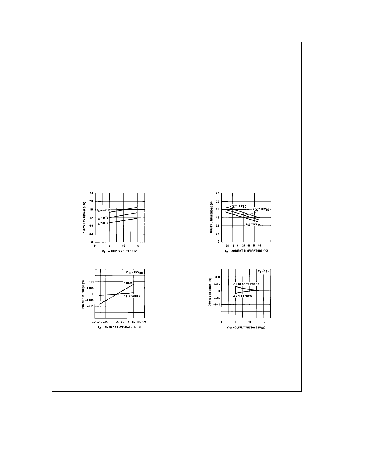
Typical Performance Characteristics
Digital Input Threshold
vs V
CC
Gain and Linearity Error
Variation vs Temperature
Digital Input Threshold
vs Temperature
Gain and Linearity Error
Variation vs Supply Voltage
TL/H/5691– 2
3
Definition of Package Pinouts
(A1–A12): Digital Inputs. A12 is the least significant digital
input (LSB) and A1 is the most significant digital input
(MSB).
I
: DAC Current Output 1. I
OUT1
digital input of all 1s, and is zero for a digital input of all 0s.
I
: DAC Current Output 2. I
OUT2
I
,orI
OUT1
voltage).
R
: Feedback Resistor. The feedback resistor is provided
Fb
on the IC chip for use as the shunt feedback resistor for the
OUT1
a
e
I
constant (for a fixed reference
OUT2
is a maximum for a
OUT1
is a constant minus
OUT2
external op amp which is used to provide an output voltage
for the DAC. This on-chip resistor should always be used
(not an external resistor) since it matches the resistors in
the on-chip R-2R ladder and tracks these resistors over
temperature.
V
: Reference Voltage Input. This input connects to an
REF
external precision voltage source to the internal R-2R ladder. V
This is also the analog voltage input for a 4-quadrant multi-
can be selected over the range of 10V tob10V.
REF
plying DAC application.
V
: Digital Supply Voltage. This is the power supply pin for
CC
the part. V
optimum for 15 V
can be from 5 VDCto 15 VDC. Operation is
CC
.
DC
GND: Ground. This is the ground for the circuit.
Definition of Terms
Resolution: Resolution is defined as the reciprocal of the
number of discrete steps in the DAC output. It is directly
related to the number of switches or bits within the DAC. For
example, the DAC1218 has 2
has 12-bit resolution.
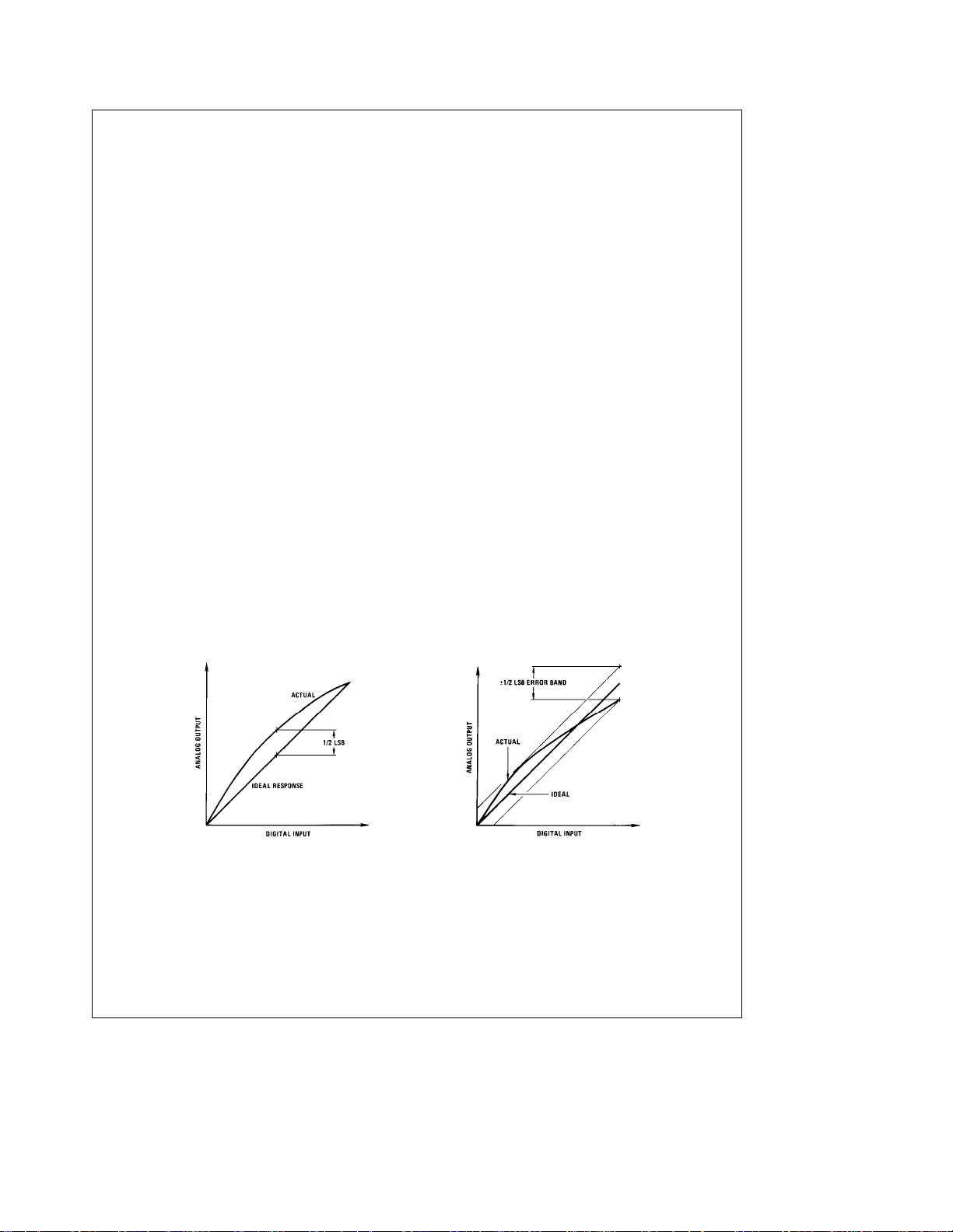
Linearity Error: Linearity error in the maximum deviation
from a
straight line passing through the endpoints of the
12
or 4096 steps and therefore
DAC transfer characteristic.
It is measured after adjusting
for zero and full scale. Linearity error is a parameter intrinsic
to the device and cannot be externally adjusted.
National’s linearity test (a) and the best straight line test (b)
used by other suppliers are illustrated below. The best
straight line (b) requires a special zero and FS adjustment
for each part, which is almost impossible for the user to
determine. The end point test uses a standard zero FS adjustment procedure and is a much more stringent test for
DAC linearity.
Power Supply Sensitivity: Power supply sensitivity is a
measure of the effect of power supply changes on the DAC
full-scale output.
Settling Time: Full-scale current settling time requires zero
to full-scale or full-scale to zero output change. Settling time
is the time required from a code transition until the DAC
output reaches within
g
1/2 LSB of the final output value.
Full-scale Error: Full-scale error is a measure of the output
error between an ideal DAC and the actual device output.
Ideally, for the DAC1218 full-scale is V
e
V
10V and unipolar operation, V
REF
e
10.0000Vb2.44 mVe9.9976V. Full-scale error is
SCALE
adjustable to zero.
REF
b
1 LSB. For
FULL-
Differential Non-Linearity: The difference between any
two consecutive codes in the transfer curve from the theoretical 1 LSB is differential non-linearity.
Monotonic: If the output of a DAC increases for increasing
digital input code, then the DAC is monotonic. A 12-bit DAC
which is monotonic to 12 bits simply means that input increasing digital input codes will produce an increasing analog output.
a) End point test after zero and FS adjust b) Shifting FS adjust to pass best straight line test
TL/H/5691– 3
4

Application Hints
The DAC1218 and DAC1219 are pin-for-pin compatible with
the DAC1220 series but feature 12 and 11-bit linearity specifications. To preserve this degree of accuracy, care must
be taken in the selection and adjustments of the output amplifier and reference voltage. Careful PC board layout is important, with emphasis made on compactness of components to prevent inadvertent noise pickup and utilization of
single point grounding and supply distribution.
1.0 BASIC CIRCUIT DESCRIPTION
Figure 1
illustrates the R-2R current switching ladder network used in the DAC1218 and DAC1219. As a function of
the logic state of each digital input, the binarily weighted
current in each leg of the ladder is switched to either I
or I
. The voltage potential at I
OUT2
at zero volts to keep the current in each leg the same, inde-
OUT1
and I
OUT2
OUT1
must be
pendent of the switch state.
The switches operate with a small voltage drop across them
and can therefore conduct currents of either polarity. This
permits the reference to be positive or negative, thereby
allowing 4-quadrant multiplication by the digital input word.
The reference can be a stable DC source or a bipolar AC
signal within the range of
an absolute maximum range of
also exceed the applied V
The maximum output current from either I
equal to
g
10V, for specified accuracy, with
g
25V. The reference can
of the DAC.
CC
V
REF(max)
4095
4096
#
,
J
R
OUT1
or I
OUT2
where R is the reference input resistance (typically 15 kX).
A high level on any digital input steers current to I
a low level steers current to I
OUT2
.
OUT1
and
2.0 CREATING A UNIPOLAR OUTPUT VOLTAGE
(A DIGITAL ATTENUATOR)
To generate an output voltage and keep the potential at the
current output terminals at 0V, an op amp current to voltage
converter is used. As shown in
I
flows through the feedback resistor, forcing a propor-
OUT1
tional voltage at the amplifier output. The voltage at I
Figure 2
held at a virtual ground potential. The feedback resistor is
provided on the chip and should always be used as it
matches and tracks the R value of the R-2R ladder. The
output voltage is the opposite polarity of the applied reference voltage.
2.1 Amplifier Considerations
To maintain linearity of the output voltage with changing
digital input codes the input offset voltage of the amplifier
must be nulled. The resistance from I
(R
) varies non-linearly with the applied digital code
I
OUT1
from a minimum of R with all ones applied to the input to
near%with an all zeros code. Any offset voltage between
the amplifier inputs appears at the output with a gain of
R
F
a
1
Since R
grade output linearity. (See Note 4 of Electrical Characteris-
is
tics.)
varies with the input code, any offset will de-
I
OUT1
R
I
OUT1
.
If the desired amplifier does not have offset balancing pins
available (it could be part of a dual or quad package) the
nulling circuit of
non-inverting input will be set to
Figure 3
can be used. The voltage at the
b
VOSinitially to force the
inverting input to 0V. The common technique of summing
current into the amplifier summing junction cannot be used
as it directly introduces a zero code output current error.
, the current from
OUT1
to ground
OUT1
is
Note: Switches shown in digital high state.
TL/H/5691– 4
FIGURE 1. The R-2R Current Switching Ladder Network
5

Application Hints (Continued)
A1
A2
A3
eb
V
OUT
where: ANe1 if digital input is high
AN
a
V
REF
2
4
#
e
0 if digital input is low
a
A12
a
...
8
4096
J
FIGURE 3. Zeroing an Amplifier Which Does Not Have Balancing Provisions
TL/H/5691– 5
FIGURE 2. Unipolar Output Voltage
TL/H/5691– 6
The selected amplifier should have as low an input bias
current as possible since input bias current contributes to
the current flowing through the feedback resistor. BI-FET
op amps such as the LF356 or LF351 or bipolar op amps
with super b input transistors like the LM11 or LM308A produce negligible errors.
2.2 Zero and Full-Scale Adjustments
The fundamental purpose is to make the output voltages as
near 0 V
of
ance, and adjusting the V
amp until the output reads zero volts. This is done, of
course, with an applied digital input of all zeros if I
driving the op amp (all ones for I
is then removed and the converter is zero adjusted.
as possible. This is accomplished in the circuit
DC
Figure 2
by shorting out the amplifier feedback resist-
nulling potentiometer of the op
OS
). The feedback short
OUT2
OUT1
A unique characteristic of these DACs is that any full-scale
or gain error is always negative. This means that for a fullscale input code the output voltage, if not inherently correct,
will always be less than what it should be. This ensures that
adding an appropriate resistance in series with the internal
feedback resistor, R
The 50X potentiometer in
, will always correct for any gain error.
Fb
Figure 2
is all that is needed to
adjust the worst case DAC gain error.
Conversion accuracy is only as good as the applied reference voltage, so providing a source that is stable over time
and temperature is important.
2.3 Output Settling Time
TM
The output voltage settling time for this circuit in response
to a change of the digital input code (a full-scale change is
the worst case) is a combination of the DAC’s output current
settling characteristics and the settling characteristics of the
output amplifier. The amplifier settling is further degraded by
a feedback pole formed by the feedback resistance and the
DAC output capacitance (which varies with the digital code).
First order compensation for this pole is achieved by adding
a feedback zero with capacitor C
shown in
C
Figure 2
.
In many applications output response time and settling is
just as important as accuracy. It can be difficult to find a
single op amp that combines excellent DC characteristics
is
(low V
settling time. BI-FET op amps offer a reasonable compro-
drift and bias current) with fast response and
OS,VOS
mise of high speed and good DC characteristics. The circuit
of
Figure 4
illustrates a composite amplifier connection that
combines the speed of a BI-FET LF351 with the excellent
DC input characteristics of the LM11. If output settling time
is not so critical, the LM11 can be used alone.
Figure 5
is a settling time test circuit for the complete voltage output DAC circuit. The circuit allows the settling time of
the DAC amplifier to be measured to a resolution of 1 mV
out of a zero to
loscope.
g
10V full-scale output change on an oscil-
Figure 6
summarizes the measured settling times
for several output amplifiers and feedback compensation
capacitors.
6

Application Hints (Continued)
Diodes are 1N4148
FIGURE 4. Composite Output Amplifier Connection
FIGURE 5. DAC Settling Time Test Circuit
Amplifier C
Settling Time to 0.01%
C
LM11 20 pF 30 ms
LF351 15 pF 8 ms
LF351 30 pF 5 ms
Composite
LM11-LF351
20 pF 8 ms
LF356 15 pF 6 ms
TL/H/5691– 7
TL/H/5691– 8
FIGURE 6. Some Measured Settling Times
7

Application Hints (Continued)
3.0 OBTAINING A BIPOLAR OUTPUT VOLTAGE
FROM A FIXED REFERENCE
The addition of a second op amp to the circuit of
can generate a bipolar output voltage from a fixed reference
voltage (
Figure 7
the MSB of the digital input word to allow two quadrant multiplication of the reference voltage. The polarity of the reference voltage can also be reversed to realize full 4-quadrant
multiplication.
The output responds in accordance to the following expression:
). This, in effect gives sign significance to
e
V
O
Db2048
V
REF
#
2048
,0sDs4095
J
Figure 2
where D is the decimal equivalent of the true binary input
word. This configuration inherently accepts a code (halfscale or D
external (/2 LSB offset as needed by other bipolar multiplying DAC circuits.
Only the offset voltage of amplifier A1 need be nulled to
preserve linearity. The gain setting resistors around A2 must
match and track each other. A thin film, 4-resistor network
available from Beckman Instruments, Inc. (part no. 694-3R10K-D) is ideally suited for this application. Two of the four
resistors can be paralleled to form R and the other two can
be used separately as the resistors labeled 2R.
Operation is summarized in the table below:
e
2048) to provide 0V out without requiring an
Applied
MSB ........ LSB
1 1 1 1 1 1 1 1 1 1 1 1 4095 V
1 1 0 0 0 0 0 0 0 0 0 0 3072 V
1 0 0 0 0 0 0 0 0 0 0 0 2048 0 0
0 1 1 1 1 1 1 1 1 1 1 1 2047
0 1 0 0 0 0 0 0 0 0 0 0 1024
0 0000000000 0 0
V
l
REF
Where 1 LSB
e
2048
*0.1% matching TL/H/5691– 9
Digital Input
l
FIGURE 7. Obtaining a Bipolar Output from a Fixed Reference
Decimal V
Equivalent
a
REF
b
b
b
V
b
REF
1 LSB
V
REF
V
REF
1 LSB
/2
/2
REF
OUT
b
V
b
V
REF
a
1 LSB
l
REF
b
V
/2
l
l
REF
a
1 LSB
a
V
/2
l
l
REF
a
V
l
l
REF
8

Application Hints (Continued)
3.1 Zero and Full-Scale Adjustments
The three adjustments needed for this circuit are shown in
Figure 7
. The first step is to set all of the digital inputs LOW
(to force I
volts at the inverting input (pin 2) of OA1. Next, with a code
of all zeros still applied, adjust ‘‘- full-scale adjust’’, the reference voltage, for V
output voltage will be opposite that of the applied reference.
Finally, set all of the digital inputs HIGH and adjust ‘‘
scale adjust’’ for V
output at this time will be the same as that of the reference
voltage. This
count the effects of the V
offset is less than 0.1% of V
external resistor mismatch.
to 0) and then trim ‘‘zero adjust’’ for zero
OUT1
e
g
(ideal V
OUT
OUT
a
full-scale adjustment scheme takes into ac-
l
e
V
REF
of amplifier A2 (as long as this
OS
REF
)l. The sign of the
REF
(511/512). The sign of the
) and any gain errors due to
a
full-
4.0 MISCELLANEOUS APPLICATION HINTS
The devices are CMOS products and reasonable care
should be exercised in handling them to prevent catastrophic failures due to electrostatic discharge.
During power-up supply voltage sequencing, the negative
supply of the output amplifier may appear first. This will typically cause the output of the op amp to bias near the negative supply potential. No harm is done to the DAC, however,
as the on-chip 15 kX feedback resistor sufficiently limits the
current flow from I
diode drop below ground.
when this lead is clamped to one
OUT1
As a general rule, any unused digital inputs should be tied
high or low as required by the application. As a troubleshooting aid, if any digital input is left floating, the DAC will
interpret that input as a logical 1 level.
Additional Application Ideas
For the circuits shown, D represents the decimal equivalent of the binary digital input code. D ranges from 0 (for an all zeros
input code) to 4095 (for an all ones input code) and for any code can be determined from:
e
D
2048(A1)a1024(A2)a512(A2)a. . . 2(A11)a1(A12)
where ANe1 if that input is high
ANe0 if that input is low
DAC Controlled Amplifier
TL/H/5691– 10
9

Additional Application Ideas (Continued)
Offsetting the Zero Code Output Voltage
2V
R2
REF
e
V
Zero Shift
R1aR2
High Current Controller
TL/H/5691– 11
I
O
1 Amp (D)
e
4096
TL/H/5691– 12
10

Additional Application Ideas (Continued)
DAC Controlled Function Generator
C1 controls maximum frequency
#
k
0.5% sine wave THD over range
#
Range 30 kHz maximum
#
LinearityÐDAC limit
#
#
e
f
4096 (4/3 RFbC)
D
C(7.5V) (4096) (R
j
PW
DlV
REF
TL/H/5691– 13
Digitally Programmable Pulse-Width Generator
)
Fb
TL/H/5691– 14
11
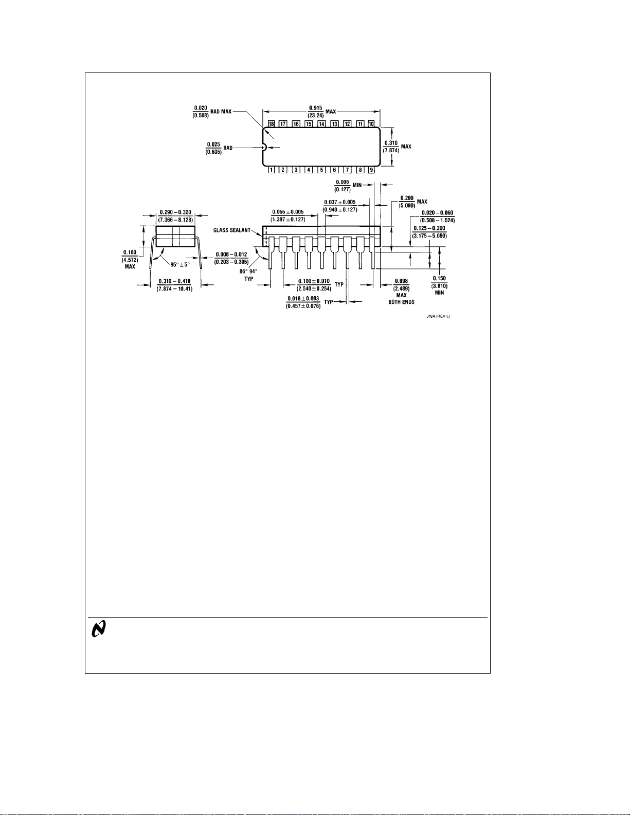
Physical Dimensions inches (millimeters)
Order Number DAC1218LCJ-1, DAC1218LCJ or DAC1219LCJ
NS Package Number J18A
DAC1218/DAC1219 12-Bit Binary Multiplying D/A Converter
LIFE SUPPORT POLICY
NATIONAL’S PRODUCTS ARE NOT AUTHORIZED FOR USE AS CRITICAL COMPONENTS IN LIFE SUPPORT
DEVICES OR SYSTEMS WITHOUT THE EXPRESS WRITTEN APPROVAL OF THE PRESIDENT OF NATIONAL
SEMICONDUCTOR CORPORATION. As used herein:
1. Life support devices or systems are devices or 2. A critical component is any component of a life
systems which, (a) are intended for surgical implant support device or system whose failure to perform can
into the body, or (b) support or sustain life, and whose be reasonably expected to cause the failure of the life
failure to perform, when properly used in accordance support device or system, or to affect its safety or
with instructions for use provided in the labeling, can effectiveness.
be reasonably expected to result in a significant injury
to the user.
National Semiconductor National Semiconductor National Semiconductor National Semiconductor
Corporation Europe Hong Kong Ltd. Japan Ltd.
1111 West Bardin Road Fax: (
Arlington, TX 76017 Email: cnjwge@tevm2.nsc.com Ocean Centre, 5 Canton Rd. Fax: 81-043-299-2408
Tel: 1(800) 272-9959 Deutsch Tel: (
Fax: 1(800) 737-7018 English Tel: (
National does not assume any responsibility for use of any circuitry described, no circuit patent licenses are implied and National reserves the right at any time without notice to change said circuitry and specifications.
Fran3ais Tel: (
Italiano Tel: (
a
49) 0-180-530 85 86 13th Floor, Straight Block, Tel: 81-043-299-2309
a
49) 0-180-530 85 85 Tsimshatsui, Kowloon
a
49) 0-180-532 78 32 Hong Kong
a
49) 0-180-532 93 58 Tel: (852) 2737-1600
a
49) 0-180-534 16 80 Fax: (852) 2736-9960
 Loading...