

查询DAC0890供应商
DAC0890
Dual 8-bit mP-Compatible Digital-to-Analog Converter
General Description
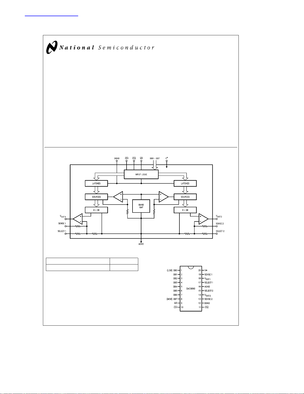
The DAC0890 is a complete dual 8-bit voltage output digitalto-analog converter that can operate on a single 5V supply.
It includes on-chip output amplifiers, precision bandgap voltage reference, and full microprocessor interface.
Each DAC0890 output amplifier has two externally selectable output ranges, 0V to 2.55V and 0V to 10.2V. The amplifiers are internally trimmed for offset and full-scale accuracy
and therefore require no external user trims.
The DAC0890 is supplied in 20-pin ceramic DIP package.
Features
Y
Two 8-bit voltage output DACs
Y
4.75V to 16.5V single operation
Block Diagram
Y
Guaranteed monotonic over temperature
Y
Internal precision bandgap reference
Y
Two calibrated output ranges; 2.55V and 10.2V
Y
2 ms settling time for full-scale output change
Y
No external trims
Y
Microprocessor interface
Applications
Y
Industrial processing controls
Y
Automotive controls
Y
Disk drive motor controls
Y
Automatic test equipment
DAC0890 Dual 8-bit mP-Compatible Digital-to-Analog Converter
May 1995
TL/H/10592– 1
Ordering Information
s
Industrial (b40§CsT
a
85§C) Package
A
Connection Diagram
Dual-In-Line Package
DAC0890CIJ J20A Cerdip
Top View
TL/H/10592– 2
C
1995 National Semiconductor Corporation RRD-B30M115/Printed in U. S. A.
TL/H/10592

Absolute Maximum Ratings (Notes1&2)
If Military/Aerospace specified devices are required,
please contact the National Semiconductor Sales
Office/Distributors for availability and specifications.
Positive Supply Voltage (V
Voltage at Any Pin (Note 3) GNDb0.3 to V
Input Current at Any Pin (Note 3) 5 mA
Package Input Current (Note 4) 20 mA
Power Dissipation (Note 5) 1.0W
ESD Susceptability (Note 6) 2000V
Output Short-Circuit Protection
Duration Indefinite
a
) 20V
a
a
0.3V
Soldering Information
J package (10 sec.) 300
Storage Temperature
b
65§Cto150§C
Junction Temperature (Note 5)
Operating Ratings (Notes1&2)
Temperature Range
s
T
MIN
DAC0890CIJ
Positive Supply Voltage, V
s
T
T
A
MAX
b
a
40§CsT
s
a
85§C
A
4.75 to 16.5V
C
§
Electrical Characteristics The following specifications apply for V
DGNDe0V, unless otherwise specified. Boldface limits apply for T
Symbol Parameter Conditions
e
e
T
A
T
J
Typical
(Note 7)
Resolution 8 Bits(min)
Monotonicity 8 Bit(min)
Integral Linearity Error
g
Fullscale Error
Zero Error
Full Scale DAC-to-DAC
Tracking (Note 9)
Analog Crosstalk V
(Note 10) V
a
e
15V, 10.2V range
a
e
5V, 2.55V range
g
Glitch Energy
(Note 11)
Digital Feedthrough
(Note 12)
t
S
I
O
I
SC
Positive Output Settling C
Time (Note 13) C
Output Current Drive (Note 14)
Capability
Output Short Circuit V
Current (Note 15)
s
500 pF 2 ms
LOAD
s
1000 pF 3 ms
LOAD
a
e
15V
PSRR Power Supply Rejection fk30 Hz
Ratio 10.2V range
(Note 16) 13.5V
2.55V range
13.5V
4.75V
4.75V
I
S
Supply Current All Inputs Low
V
V
V
ILD
V
IHD
V
ILC
Data Logic Low Threshold 0.8 V (max)
Data Logic High Threshold 2.0 V (min)
Control Logic Low
Threshold
a
s
s
V
16.5V 7 15 ppm/% (max)
a
s
s
V
16.5V 4 59 ppm/% (max)
a
s
s
V
5.25V 4 20 ppm/% (max)
a
s
s
V
16.5V 4 ppm/%
a
e
16.5 25 30/35 mA (max)
a
e
4.75 23 mA
a
MIN
0.16
ea
to T
MAX
a
5V and V
ea
15V and AGND
; all other limits T
A
Limit
(Note 8)
g
0.5 LSB(min)
g
1.5/g2.5 LSB(max)
g
1.0/g2.0 LSB(max)
e
T
J
Units
0.25 LSB
b
74 dB
b
66 dB
45 V-ns
60 V-ns
85/3.5 mA(min)
20 mA
0.8 V (max)
e
e
25§C.
2
Electrical Characteristics (Continued)
The following specifications apply for V
Boldface limits apply for T
Symbol Parameter Conditions
V
IHC
A
Control Logic High
Threshold
a
e
ea
e
T
T
MIN
to T
J
5V and V
; all other limits T
MAX
a
ea
15V and AGNDeDGNDe0V, unless otherwise specified.
e
e
T
J
Typical
(Note 7)
25§C.
Limit
(Note 8)
A
Units
2.2 V (min)
Digital Input Current (Note 17) 2.2 25 mA (max)
t
WR
t
DS
t
DH
t
CS
t
CH
Note 1: Absolute Maximum Ratings indicate limits beyond which damage to the device may occur. DC and AC electrical specifications do not apply when operating
the device beyond its specified operating ratings. Operating Ratings indicate conditions for which the device is functional, but do not guarantee performance limits.
For guaranteed specifications and test conditions, see the Electrical Characteristics. The guaranteed specifications apply only for the test conditions listed. Some
performance characteristics may degrade when the device is not operated under the listed test conditions.
Note 2: All voltages are measured with respect to AGND, unless otherwise specified.
Note 3: When the input voltage (V
limited to 5 mA or less.
Note 4: The sum of the currents at all pins that are driven beyond the power supply voltages should not exceed 20 mA.
Note 5: The maximum power dissipation must be derated at elevated temperatures and is dictated by T
allowable power dissipation at any temperature is P
(§C) and iJA(§C/W) for the DAC0890CIJ are 125§C and 53§C/W, respectively.
T
JMAX
Part Number T
DAC0890CIJ 125 53
Note 6: Human body model, 100 pF discharged through a 1.5 kX resistor.
Note 7: Typicals are at 25
Note 8: Guaranteed to National’s AOQL (Average Outgoing Quality Level).
Note 9: Full Scale DAC-to-DAC Tracking is defined as the change in the voltage difference between the full scale output levels of DAC1 and DAC2. The result is
expressed in LSBs and it referred to the full-scale voltage difference at 25
Note 10: Analog Crosstalk is a measure of the change in one DAC’s full scale output voltage as the second DAC’s output voltage changes value. It is measured as
the voltage change in one DAC’s full scale output voltage divided by the voltage range through which the second DAC’s output has changed (zero to full scale).
This ratio is then expressed in dB.
Note 11: Glitch Energy is a worst case measurement, over the entire input code range, of transients that occur when changing code. The positive and negative
areas of the transient waveforms are summed together to obtain the value listed.
Note 12: Digital Feedthrough is measured with both DAC outputs latched at full scale and a 2 ns, 5V step applied to all 8 data inputs. This gives the worst case
digital feedthrough for the DAC0890.
Note 13: Settling Time is specified for a positive full scale step to
pull-down resistor. Negative settling time to
)(R
(C
LOAD
LOAD
Note 14: Output Current Drive Capability is the minimum current that can be sourced by the output amplifiers with less than (/2 LSB reduction in full scale. Current
sinking capability is provided by a passive internal resistance of 10 kX in the high range and 2.5 kX in the low range.
Note 15: Output Short Circuit Current is measured with the output at full-scale and shorted to AGND.
Note 16: Power Supply Rejection Ratio is a measure of how much the output voltage changes (in parts-per-million) per change (in percent) in the power supply
voltage.
Note 17: Digital Input Current is measured with 0V and V
Write Time 18 40 ns (min)
Data Setup Time 18 35 ns (min)
Data Hold Time 3 ns (max)
Control Setup Time 18 40 ns (min)
Control Hold Time 0 ns (max)
) at any pin exceeds the power supply rails (V
IN
e
(T
D
(§C) iJA(§C/W)
JMAX
C, unless otherwise specified, and represent the most likely parametric norm.
§
g
/2.5 kX) for the low range.
(/2 LSB can be calculated for each range where t
a
)/iJAor the number given in the Absolute Maximum Ratings, whichever is lower. The
JMAX-TA
C.
§
g
(/2 LSB. Settling time for negative steps will be slower but may be improved with an external
input levels. The limit specified is the higher of these two measurements.
k
IN
AGND or V
l
Va) the absolute value of current at that pin should be
IN
, iJAand the ambient temperature, TA. The maximum
JMAX
e
6.23 (C
S
LOAD
)(R
/10 kX ) for the high range and t
LOAD
e
6.23
S
3
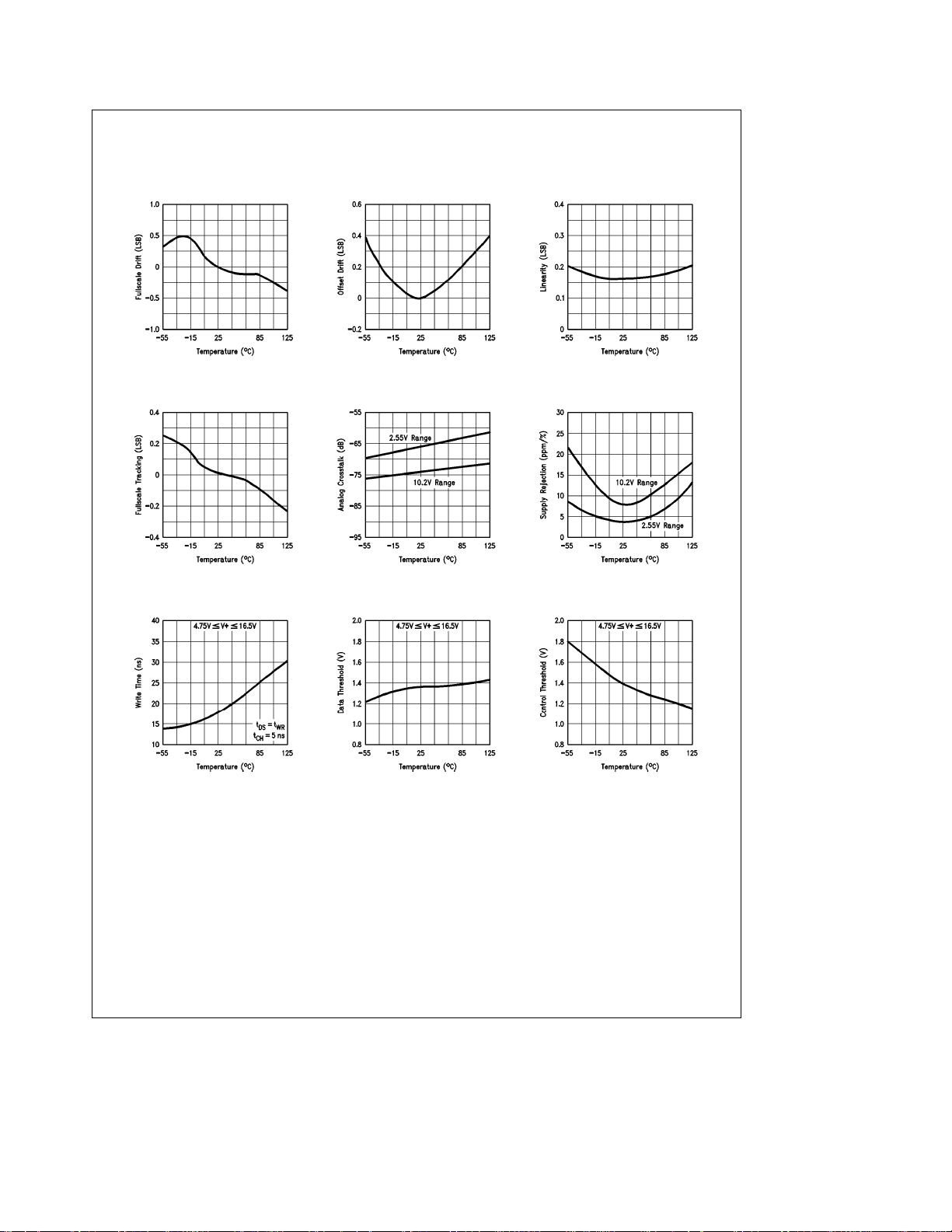
Typical Performance Characteristics
Fullscale Drift
vs Temperature
Fullscale Dac to Dac
Tracking
vs Temperature
Write Time
vs Temperature
Offset Drift
vs Temperature
Analog Crosstalk
vs Temperature
Data Threshold
vs Temperature
Integral Linearity
vs Temperature
Power Supply Rejection
vs Temperature
Control Threshold
vs Temperature
TL/H/10592– 3
4

Typical Performance Characteristics
Supply Current
vs Temperature
Minimum Supply Voltage
vs Temperature
(10.2V Range)
Short Circuit Current
vs Temperature
Minimum Supply Voltage
vs Temperature
(2.55V Range)
Power Supply Rejection
vs Frequency
Digital Input Current
vs Temperature
Max Power Dissipation
vs Temperature
TL/H/10592– 4
5

Timing Waveforms
TL/H/10592– 5
6

Connection Diagram
Dual-In-Line Package
Pin Description
DB0–DB7 (1 –8) These pins are data inputs for each of the
WR
(9) This is the WRITE command input pin.
CS1
(10) This is the input pin used to select DAC1.
CS2 (11) This is the input pin used to select DAC2.
DGND (12) The system digital ground is connected to
SENSE 2 (13) DAC2’s output sense connection. When
internal 8-bit DACs. DB0 is the least-significant-bit.
This input is used in conjunction with CS1
and CS2 to write data into either of the
internal DACs. The data is latched into a
selected DAC with the rising edge of either WR
DAC2, whichever occurs first.
This input is used in conjunction with the
WR
internal DACs. The data is latched into
DAC1 with the rising edge of either CS1
WR
This input is used in conjunction with the
WR
internal DACs. The data is latched into
DAC2 with the rising edge of either CS2
WR
this pin. For proper operation, this and
AGND must be connected together.
this pin is connected to the VOUT2’s load
impedance, the feedback loop will compensate for any voltage drops between
the VOUT2 pin and the load.
or CS1 for DAC1 or CS2 for
input to write data into either of the
, whichever occurs first.
input to write data into either of the
, whichever occurs first.
TL/H/10592– 2
V
(14) DAC2’s voltage output connection. It pro-
OUT2
SELECT 2 (15) The two output voltage ranges available
AGND (16) The system digital ground is connected to
SELECT 1 (17) The two output voltage ranges available
or
V
(18) DAC1’s voltage output connection. It pro-
OUT1
or
SENSE 1 (19) DAC1’s output sense connection. When
a
V
(20) The power supply voltage, ranging from
vides two full-scale output voltage ranges,
2.55V and 10.2V.
from DAC2 are selected by connecting
this pin to SENSE2 for the 2.55V full-scale
range and leaving it unconnected for the
10.2V full-scale range.
this pin. For proper operation, this and
DGND must be connected together.
from DAC1 are selected by connecting
this pin to SENSE1 for he 2.55V full-scale
range and leaving it unconnected for the
10.2V full-scale range.
vides two full-scale output voltage ranges,
2.55V and 10.2V.
this pin is connected to the VOUT1’s load
impedance, the feedback loop will compensate for any voltage drops between
the VOUT1 pin and the load.
4.75V to 16.5V, is applied to this pin. It
should be bypassed, to AGND, with a 0.01
E
0.1 mF ceramic capacitor in parallel
with a 2.2E22 m F electrolytic capacitor.
7

Functional Description
The DAC0890 is a monolithic dual 8-bit bipolar Digital-to-Analog converter comprising six major functional blocks designed to operate on a single supply as low as 5V (
These include two latch/DAC combinations, two high-speed
output amplifiers, band-gap reference, and control/interface
logic.
The two internal 8-bit DACs use equal valued current sources. Controlled by a corresponding bit in the input data, each
current source’s output is switched into either an R/2R ladder or AGND. Each internal DAC has an 8-bit latch to store
a digital input. See
The high-speed output amplifiers operate in the non-inverting mode. The R-2R’s output current is applied to the output
amplifier and converted to a voltage. The amplifier’s gain is
Figure 1
.
g
5%).
externally set through the range select pin. The two ranges
are 0V to 2.55V and 0V to 10.2V. The internal resistors that
set the gain are matched to the unit resistor of the R/2R
ladder. This ensures that these resistors match over process variations and temperature. This greatly reduces gain
variations that would exist if external gain setting resistors
were used.
An internal band-gap reference and its control amplifier generate a full scale reference voltage for the DACs. It produces a 1.2V output from a single supply.
The DAC0890 provides a TTL and CMOS-compatible control interface and allows writing and latching digital values to
each of the internal DACs.
FIGURE 1. Simplified Internal Schematic (One DAC Shown)
8
TL/H/10592– 7

Applications Information
Full-Scale Output Voltage Range Selection
The DAC0890 has been designed for ease of use. All reference voltage and output amplifier connections are internal.
All trims such as full-scale (gain) and zero (offset) are performed during manufacturing. Therefore, no external trimming is required to achieve the specified accuracy. The only
external connections required select the desired full-scale
output voltage range.
The two full-scale output voltage ranges are selected by
connecting SENSE, SELECT and VOUT as shown in
2a
,b. The 2.55V range can be used with supply voltages as
low as 4.75V. The 10.2V range can be selected with supplies as low as 12.0V.
FIGURE 2a. 0V to 2.55V Output Voltage Range
Figure
TL/H/10592– 8
Grounding and Power Supply
Bypassing
Proper grounding is essential to extract all the precision and
full rated performance that the DAC0890 is capable of delivering. Typical applications for the DAC0890 include operation with a microprocessor. In this environment digital noise
is prevalent and anticipated. Therefore, special care must
be taken to ensure that proper operation will be achieved.
The DAC0890 uses two ground pins, AGND and DGND, to
minimize ground drops and noise in the analog signal paths.
Figure 3
details the proper bypassing and ground connec-
tions.
The DAC0890’s best performance can be ensured by connecting 0.01 mFto0.1mF ceramic capacitor in parallel with
an electrolytic of 2.2 mFto22mF between the V
AGND.
a
pin and
Sense Inputs
The SENSE inputs (pins 13 and 19) allow compensation for
voltage drops in long output lines to remote loads. This
places the drops in the internal amplifier’s feedback loop.
An example of this is shown in
might be caused by printed circuit board traces or long cables, between the VOUT2 and the load impedance R
placed inside the feedback loop if SENSE1 is connected
directly to the load. This forces the voltage at the load to be
the correct value. It is important to remember that the voltage at the DAC0890’s VOUT pins may become higher than
the full-scale output voltage selected using the SELECT
pins. Therefore, the power supply voltage applied to V
must bet2.2V above the resulting output voltage (at pins
14 and 18) when the SENSE inputs are used.
The SENSE inputs have a finite input impedance. The
range-setting resistors load the output with 2.5 kX when the
0V to 2.55V range is selected and 10 kX when the 0V to
10.2V range is selected.
Figure 3
. The I-R drop, which
L
is
a
FIGURE 2b. 0V to 10.2V Output Voltage Range
TL/H/10592– 9
Power Supply Voltage
The DAC0890 is designed to operate on a single power
supply voltages
operation the power supply voltage can be as low as
a
4.75V. When the 10.2V full-scale is used the supply volt-
age needs to be between
a
4.75V anda16.5V. For 2.55V full-scale
a
12V toa16.5V.
FIGURE 3. Typical Connection Showing Power Supply
TL/H/10592– 10
Bypassing, and the Use of SENSE Inputs
9

Minimizing Settling Time
The DAC0890’s output stage uses a passive pull-down resistor to achieve single supply operation and an output voltage range that includes ground. This results in a negativegoing settling time that is longer than the settling time or
positive-going signals. The actual settling time is dependant
on the load resistance and capacitance. If available, a negative power supply can be used to improve the negative settling time by connecting a pull down resistor between the
output and the negative supply. The resistor’s value is chosen so that the current through the pull down resistor is not
greater than 0.5 mA when the output voltage is 0V. See
Figure 4
.
FIGURE 4. Improving Negative Slew Rate
TL/H/10592– 11
Bipolar Operation
While the DAC0890 was designed to operate on a single
positive supply voltage and generate a unipolar output voltage, bipolar operation is still possible if a negative supply is
available or added. As shown in
Figure 5
, the output voltage
is offset and scaled to achieve a
range with the addition of a
is generated with an LM385 –1.2V reference. The external
output amplification is provided by the LMC660. The output
voltage is generated with a complementary binary offset input code.
b
1.27V toa1.28V output
b
5V supply. The required offset
Microprocessor Interface
When interfacing with a microprocessor, the DAC0890 appears as a two byte write-only memory location for memory
mapped and I/O mapped input-output. Each of the internal
DACs is chosen through one of the two chips selects, CS1
or CS2. The action of the control signals is detailed in Table
I. The data is latched on the rising edge of either Chip Select or WR
For interfacing ease, WR
can be used to latch the data. Both DACs can be updated
simultaneously by pulling both CS1
versatility is provided by the ability of WR
CS2
, whichever occurs first for a given selected DAC.
to be tied together.
TABLE I. DAC0890 Control Logic Truth Table
Input
WR
Data Condition
0 0 0 0 ‘‘transparent’’
1 0 0 1 ‘‘transparent’’
0
u
1
u
00
10
X 1 X previous data latching
X X 1 previous data latching
X 1 1 previous data latching
can be tied low and CS1 or CS2
and CS2 low. Further
and CS1 and/or
CS DAC Data
0 0 latching
0 1 latching
u
u
0 latching
1 latching
Latch
FIGURE 5. Bipolar Operation
10
TL/H/10592– 12

11

Physical Dimensions inches (millimeters)
Cerdip Dual-In-Line Package (J)
Order Number DAC0890CIJ
NS Package Number J20A
DAC0890 Dual 8-bit mP-Compatible Digital-to-Analog Converter
LIFE SUPPORT POLICY
NATIONAL’S PRODUCTS ARE NOT AUTHORIZED FOR USE AS CRITICAL COMPONENTS IN LIFE SUPPORT
DEVICES OR SYSTEMS WITHOUT THE EXPRESS WRITTEN APPROVAL OF THE PRESIDENT OF NATIONAL
SEMICONDUCTOR CORPORATION. As used herein:
1. Life support devices or systems are devices or 2. A critical component is any component of a life
systems which, (a) are intended for surgical implant support device or system whose failure to perform can
into the body, or (b) support or sustain life, and whose be reasonably expected to cause the failure of the life
failure to perform, when properly used in accordance support device or system, or to affect its safety or
with instructions for use provided in the labeling, can effectiveness.
be reasonably expected to result in a significant injury
to the user.
National Semiconductor National Semiconductor National Semiconductor National Semiconductor
Corporation Europe Hong Kong Ltd. Japan Ltd.
1111 West Bardin Road Fax: (
Arlington, TX 76017 Email: cnjwge@tevm2.nsc.com Ocean Centre, 5 Canton Rd. Fax: 81-043-299-2408
Tel: 1(800) 272-9959 Deutsch Tel: (
Fax: 1(800) 737-7018 English Tel: (
National does not assume any responsibility for use of any circuitry described, no circuit patent licenses are implied and National reserves the right at any time without notice to change said circuitry and specifications.
Fran3ais Tel: (
Italiano Tel: (
a
49) 0-180-530 85 86 13th Floor, Straight Block, Tel: 81-043-299-2309
a
49) 0-180-530 85 85 Tsimshatsui, Kowloon
a
49) 0-180-532 78 32 Hong Kong
a
49) 0-180-532 93 58 Tel: (852) 2737-1600
a
49) 0-180-534 16 80 Fax: (852) 2736-9960
 Loading...