

查询DAC0854供应商
DAC0854 Quad 8-Bit Voltage-Output
Serial D/A Converter with Readback
DAC0854 Quad 8-Bit Voltage-Output Serial D/A Converter with Readback
January 1995
General Description
The DAC0854 is a complete quad 8-bit voltage-output digital-to-analog converter that can operate on a single 5V supply. It includes on-chip output amplifiers, internal voltage reference, and a serial microprocessor interface. By combining
in one package the reference, amplifiers, and conversion
circuitry for four D/A converters, the DAC0854 minimizes
wiring and parts count and is hence ideally suited for applications where cost and board space are of prime concern.
The DAC0854 also has a data readback function, which can
be used by the microprocessor to verify that the desired
input word has been properly latched into the DAC0854’s
data registers. The data readback function simplifies the design and reduces the cost of systems which need to verify
data integrity.
The logic comprises a MICROWIRE
TM
-compatible serial interface and control circuitry. The interface allows the user to
write to any one of the input registers or to all four at once.
The latching registers are double-buffered, consisting of 4
separate input registers and 4 DAC registers. Double buffering allows all 4 DAC outputs to be updated simultaneously.
The four reference inputs allow the user to configure the
system to have a separate output voltage range for each
DAC. The output voltage of each DAC can range between
0.3V and 2.8V and is a function of V
input word.
BIAS,VREF
, and the
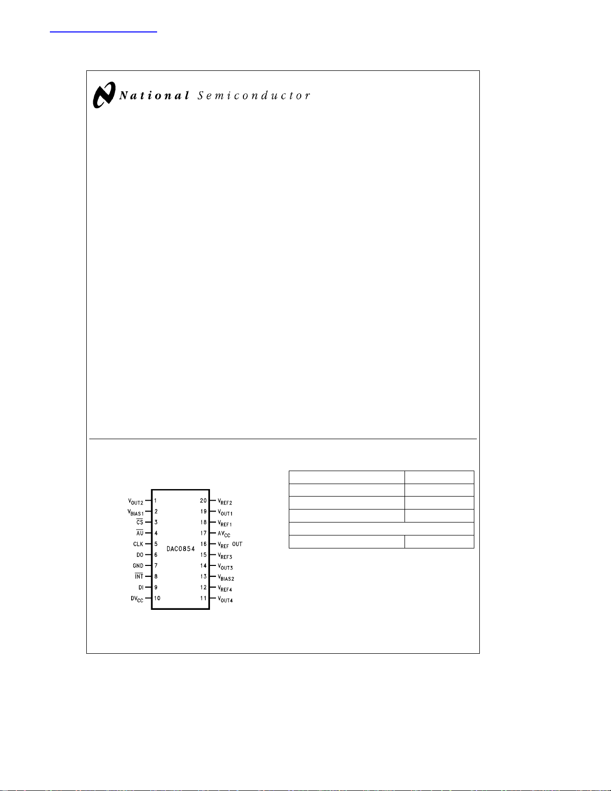
Connection Diagram
Features
Y
Singlea5V supply operation
Y
MICROWIRE serial interface allows easy interface to
many popular microcontrollers including the COPS
and HPCTMfamilies of microcontrollers
Y
Data readback capability
Y
Output data can be formatted to read back MSB or
LSB first
Y
Versatile logic allows selective or global update of the
DACs
Y
Power fail flag
Y
Output amplifiers can drive 2 kX load
Y
Synchronous/asynchronous update of the DAC outputs
Key Specifications
Y
Guaranteed monotonic over temperature
Y
Integral linearity error
Y
Output settling time 2.7 ms max
Y
Analog output voltage range 0.3V to 2.8V
Y
Supply voltage range 4.5V to 5.5V
Y
Clock frequency 10 MHz max
Y
Power dissipation (f
Y
On-board reference 2.65Vg2% max
e
10 MHz) 95 mW max
CLK
g
(/2 LSB max
Applications
Y
Automatic test equipment
Y
Industrial process controls
Y
Automotive controls and diagnostics
Y
Instrumentation
Ordering Information
TM
Industrial (b40§CkT
a
85§C) Package
A
DAC0854BIN, DAC0854CIN N20A Molded DIP
DAC0854CIJ J20A Ceramic DIP
DAC0854BIWM, DAC0854CIWM M20B Small Outline
k
Military (b55§CkT
a
125§C)
A
DAC0854CMJ/883 J20A Ceramic DIP
Top View
TL/H/11261– 1
COPSTM, HPCTMand MICROWIRETMare trademarks of National Semiconductor Corporation.
C
1995 National Semiconductor Corporation RRD-B30M75/Printed in U. S. A.
TL/H/11261
Absolute Maximum Ratings (Notes1&2)
If Military/Aerospace specified devices are required,
please contact the National Semiconductor Sales
Office/Distributors for availability and specifications.
(Note 24)
Supply Voltage (AV
Supply Voltage Difference (AV
Voltage at Any Pin (Note 3) GNDb0.3V to
Input Current at Any Pin (Note 3) 5 mA
Package Input Current (Note 4) 20 mA
Power Dissipation (Note 5) 105 mW
ESD Susceptibility (Note 6) 1250V
,DVCC)7V
CC
CC
–DVCC)
AV
CC
/DV
CC
g
5.5V
a
0.3V
Soldering Information
J Package (10 sec.) 300
N Package (10 sec.) 260
SO Package
Vapor Phase (60 sec.) 215
Infrared (15 sec.) (Note 7) 220
Storage Temperature
b
65§Ctoa150§C
Operating Ratings (Notes1&2)
Supply Voltage 4.5V to 5.5V
Supply Voltage Difference (AV
Temperature Range T
DAC0854BIN, DAC0854CIN,
DAC0854CIJ, DAC0854BIWM,
DAC0854CIWM
DAC0854CMJ/883
CC
b
DVCC)
b
b
55§CkT
k
MIN
40§CkT
g
k
T
T
A
MAX
k
85§C
A
k
125§C
A
C
§
C
§
C
§
C
§
IV
Converter Electrical Characteristics
e
The following specifications apply for AV
the analog outputs – pins 1, 11, 14, and 19) and f
e
TJfrom T
MIN
to T
. All other limits apply for T
MAX
CC
Symbol Parameter Conditions
STATIC CHARACTERISTICS
n Resolution f
Monotonicity (Note 10) 8 8 bits
Integral Linearity Error (Note 11)
DAC0854BIN, DAC0854BIWM
DAC0854CIN, DAC0854CIJ,
DAC0854CIWM, DAC0854CMJ
Differential Linearity Error
Fullscale Error (Note 12)
Fullscale Error Tempco (Note 13)
Zero Error (Note 14)
Zero Error Tempco (Note 13)
Power Supply Sensitivity (Note 15)
DYNAMIC CHARACTERISTICS
t
a
s
t
b
s
Positive Voltage Output (Note 16)
Settling Time C
Negative Voltage Output (Note 16)
Settling Time C
Digital Crosstalk (Note 17) 1.8 mV
Digital Feedthrough (Note 18) 8.5 mV
Clock Feedthrough (Note 19) 3.3 mV
Channel-to-Channel Isolation (Note 20)
Glitch Energy (Note 21) 7 nVbs
Peak Value of Largest Glitch 38 mV
PSRR Power Supply Rejection Ratio (Note 22)
DV
e
5V, V
CC
CLK
REF
e
10 MHz unless otherwise specified. Boldface limits apply for T
e
25§C.
A
CLK
L
L
e
2.65V, V
BIAS
e
1.4V, R
e
2kX(RLis the load resistor on
L
Typical Limit Units
(Note 8) (Note 9) (Limits)
e
10 MHz 8 8 bits
g
0.5 LSB (max)
g
1.0 LSB (max)
g
1.0 LSB (max)
g
35 mV
b
30 ppm/§C
g
35 mV
b
30 ppm/§C
e
e
200 pF
200 pF
b
42
1.5 2.1 ms
1.8 2.7 ms
b
78 dB
b
49 dB
b
34 dB (max)
A
p-p
p-p
p-p
2
Converter Electrical Characteristics (Continued)
e
e
DV
The following specifications apply for AV
the analog outputs – pins 1, 11, 14, and 19) and f
e
TJfrom T
MIN
to T
. All other limits apply for T
MAX
CC
CC
CLK
5V, V
e
Symbol Parameter Conditions
DIGITAL AND DC ELECTRICAL CHARACTERISTICS
V
IN(1)
V
IN(0)
I
IL
C
IN
C
OUT
V
OUT(1)
V
OUT(0)
V
INT
I
S
Logical ‘‘1’’ Input Voltage AV
Logical ‘‘0’’ Input Voltage AV
CC
CC
Digital Input Leakage Current 1 5 mA (max)
Input Capacitance 4 pF
Output Capacitance 5 pF
Logical ‘‘1’’ Output Voltage I
Logical ‘‘0’’ Output Voltage I
SOURCE
e
SINK
Interrupt Pin Output Voltage 10 kX Pullup 0.4 V (max)
Supply Current Outputs Unloaded 14 19 mA
REFERENCE INPUT CHARACTERISTICS
V
REF
R
REF
C
REF
V
INPUT CHARACTERISTICS
BIAS
V
BIAS
Input Voltage Range 0–2.75 V
Input Resistance 7 4 kX (min)
Input Capacitance Full-Scale Data Input 40 pF
V
Input Voltage Range 0.3–1.4 V
BIAS
Input Leakage 1 mA
C
BIAS
BANDGAP REFERENCE CHARACTERISTICS (C
V
OUT Output Voltage 2.65g2% V
REF
DV
REF
Input Capacitance 9 pF
e
220mF)
L
/DT Tempco (Note 23) 22 ppm/§C
Line Regulation 4.5VkV
DV
/DILLoad Regulation 0kI
REF
I
SC
Short Circuit Current V
L
k
0
I
L
b
1kI
OUTe0V 12 mA
REF
AC ELECTRICAL CHARACTERISTICS
t
t
t
t
t
t
t
DS
DH
CS
CH
MIN
H
L
Data Setup Time 10 ns (min)
Data Hold Time 0 ns (min)
Control Setup Time 15 ns (min)
Control Hold Time 0 ns (min)
Clock Frequency 10 MHz (max)
Minimum Clock High Time 20 ns (min)
Minimum Clock Low Time 40 ns (min)
e
2.65V, V
REF
10 MHz unless otherwise specified. Boldface limits apply for T
e
25§C.
A
BIAS
e
1.4V, R
e
2kX(RLis the load resistor on
L
Typical Limit Units
(Note 3) (Note 4) (Limits)
e
e
DV
5.5V 2.0 V (min)
CC
e
e
DV
4.5V 0.8 V (max)
CC
e
0.8 mA 2.4 V (min)
3.2 mA 0.4 V (max)
10 kX (max)
k
CC
k
4mA 2 6 mV
k
4 mA; CMJ Suffix 2 15 mV
k
0 mA 2.5 mV
L
5.5V, I
e
4mA 2 5 mV
L
A
3
Converter Electrical Characteristics (Continued)
e
e
DV
The following specifications apply for AV
the analog outputs – pins 1, 11, 14, and 19) and f
e
TJfrom T
MIN
to T
. All other limits apply for T
MAX
CC
CC
CLK
5V, V
e
Symbol Parameter Conditions
AC ELECTRICAL CHARACTERISTICS (Continued)
t
CZ1
t
CZ0
t
1H
t
0H
Note 1: Absolute Maximum Ratings indicate limits beyond which damage to the device may occur. Operating Ratings indicate conditions for which the device is
functional. These ratings do not guarantee specific performance limits, however. For guaranteed specifications and test conditions, see the Converter Electrical
Characteristics. The guaranteed specifications apply only for the test conditions listed. Some performance characteristics may degrade when the device is not
operated under the listed test conditions.
Note 2: All voltages are measured with respect to ground, unless otherwise specified.
Note 3: When the input voltage (V
to 5 mA or less.
Note 4: The sum of the currents at all pins that are driven beyond the power supply voltages should not exceed 20 mA.
Note 5: The maximum power dissipation must be derated at elevated temperatures and is dictated by T
(package junction to ambient thermal resistance), and TA(ambient temperature). The maximum allowable power dissipation at any temperature is
e
(T
P
Dmax
packages and versions of the DAC0854.
Note 6: Human body model, 100 pF discharged through a 1.5 kX resistor.
Note 7: See AN450 ‘‘Surface Mounting Methods and Their Effect on Production Reliability’’ of the section titled ‘‘Surface Mount’’ found in any current Linear
Databook for other methods of soldering surface mount devices.
Note 8: Typicals are at T
Note 9: Limits are guaranteed to National’s AOQL (Average Outgoing Quality Level).
Note 10: A monotonicity of 8 bits for the DAC0854 means that the output voltage changes in the same direction (or remains constant) for each increase in the input
code.
Note 11: Integral linearity error is the maximum deviation of the output from the line drawn between zero and full-scale (excluding the effects of zero error and fullscale error).
Note 12: Full-scale error is measured as the deviation from the ideal 2.800V full-scale output when V
Note 13: Full-scale error tempco and zero error tempco are defined by the following equation:
where Error (T
voltage span of the DAC0854, which depends on V
Note 14: Zero error is measured as the deviation from the ideal 0.310V output when V
Note 15: Power Supply Sensitivity is the maximum change in the offset error or the full-scale error when the power supply differs from its optimum 5V by up to
0.25V (5%). The load resistor R
Note 16: Positive or negative settling time is defined as the time taken for the output of the DAC to settle to its final full-scale or zero output to within
This time shall be referenced to the 50% point of the positive edge of CS
Note 17: Digital crosstalk is the glitch measured on the output of one DAC while applying an all 0s to all 1s transition at the input of the other DACs.
Note 18: All DACs have full-scale outputs latched and DI is clocked with no update of the DAC outputs. The glitch is then measured on the DAC outputs.
Note 19: Clock feedthrough is measured for each DAC with its output at full-scale. The serial clock is then applied to the DAC at a frequency of 10 MHz and the
glitch on each DAC full-scale output is measured.
Note 20: Channel-to-channel isolation is a measure of the effect of a change in one DAC’s output on the output of another DAC. The V
between 1.4V and 2.65V at a frequency of 15 kHz while the change in full-scale output of the second DAC is measured. The first DAC is loaded with all 0s.
Note 21: Glitch energy is the difference between the positive and negative glitch areas at the output of the DAC when a 1 LSB digital input code change is applied
to the input. The glitch energy will have its largest value at one of the three major transitions. The peak value of the maximum glitch is separately specified.
Note 22: Power Supply Rejection Ratio is measured by varying AV
of this signal imposed on a full-scale output of the DAC under consideration.
Note 23: The bandgap reference tempco is defined by the following equation:
where T
Note 24: A Military RETS specification is available upon request.
Jmax
ROOM
Output Hi-Z to Valid 1 37 ns (max)
Output Hi-Z to Valid 0 42 ns (max)
CS to Output Hi-Z 10 kX with 60 pF 130 ns (max)
CS to Output Hi-Z 10 kX with 60 pF 117 ns (max)
) at any pin exceeds the power supply rails (V
IN
b
TA)/HJAor the number given in the Absolute Maximum Ratings, whichever is lower. The table below details T
Part Number T
DAC0854BIN, DAC0854CIN 125 46
DAC0854BIJ, DAC0854CIJ 125 53
DAC0854BIWM, DAC0854CIWM 125 64
DAC0854CMJ/883 150 53
e
25§C and represent most likely parametric norm.
J
Error (T
) is the zero error or full-scale error at T
MAX
e
5kX.
L
e
25§C, V
) is the reference output at T
REF(TMAX
Error tempco
BIAS
Tempco
e
Ð
(in volts), and Error (T
MAX
and V
.
REF
e
CC
V
REF(TMAX
e
Ð
MAX
V
, and similarly for V
e
2.65V, V
REF
10 MHz unless otherwise specified. Boldface limits apply for T
e
25§C.
A
BIAS
e
1.4V, R
e
2kX(RLis the load resistor on
L
Typical Limit Units
(Note 3) (Note 4) (Limits)
k
IN
)bError (T
MAX
V
SPAN
MIN
, which initiates the update of the analog outputs.
DVCCbetween 4.75V and 5.25V with a frequency of 10 kHz and measuring the proportion
)bV
REF(TMIN
REF(TROOM
)
l
GND or V
Jmax
REF
Va) the absolute value of current at that pin should be limited
IN
Jmax
(§C) HJA(§C/W)
e
2.650V and V
REF
T
MAX
2.650V, V
10
T
MAX
) and V
6
10
b
T
(
MIN
e
1.400V, and the digital input word is all zeros.
BIAS
6
b
T
(
MIN
REF(TROOM
).
)
MIN
(Ð
) is the zero error or full-scale error at T
e
)
(Ð
REF(TMIN
(maximum junction temperature), H
and HJAfor the various
Jmax
e
1.400V.
BIAS
MIN
(in volts); V
REF
is the output
SPAN
of the first DAC is varied
g
0.5 LSB.
A
JA
4
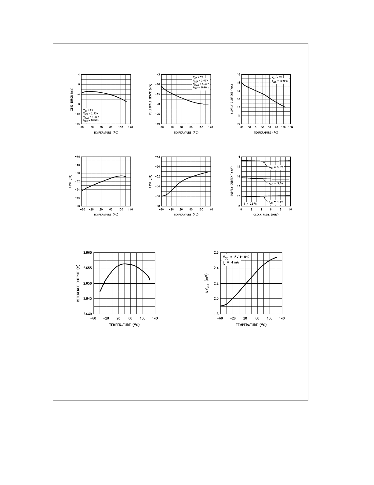
Typical Converter Performance Characteristics
Zero Error vs
Temperature
Zero Error PSRR
vs Temperature
Full-Scale Error
vs Temperature
Full-Scale Error PSRR
vs Temperature
Typical Reference Performance Characteristics
Supply Current
vs Temperature
Supply Current vs
Clock Frequency
TL/H/11261– 2
Bandgap Voltage
vs Temperature
TL/H/11261– 3
Line Regulation
vs Temperature
TL/H/11261– 4
5
 Loading...